 | –≠–ª–µ–∫—Ç—Ä–æ–Ω–Ω—ã–π –∫–æ–º–ø–æ–Ω–µ–Ω—Ç: LM106H | –°–∫–∞—á–∞—Ç—å:  PDF PDF  ZIP ZIP |
LM106/LM306
Voltage Comparator
General Description
The LM106 series are high-speed voltage comparators de-
signed to accurately detect low-level analog signals and
drive a digital load. They are equivalent to an LM710, com-
bined with a two input NAND gate and an output buffer. The
circuits can drive RTL, DTL or TTL integrated circuits directly.
Furthermore, their outputs can switch voltages up to 24V at
currents as high as 10 mA.
The devices have short-circuit protection which limits the in-
rush current when it is used to drive incandescent lamps, in
addition to preventing damage from accidental shorts to the
positive supply. The speed is equivalent to that of an LM710.
However, they are even faster where buffers and additional
logic circuitry can be eliminated by the increased flexibility of
the LM106 series. They can also be operated from any
negative supply voltage between -3V and -12V with little ef-
fect on performance.
The LM106 is specified for operation over the -55∞C to
+125∞C military temperature range. The LM306 is specified
for operation over 0∞C to +70∞C temperature range.
Features
n
Improved accuracy
n
Fan-out of 10 with DTL or TTL
n
Added logic or strobe capability
n
Useful as a relay or lamp driver
n
Plug-in replacement for the LM710
n
40 ns maximum response time
December 1994
LM106/LM306
V
oltage
Comparator
LM106/LM306
© 1997 National Semiconductor Corporation
DS007756
www.national.com
1
PrintDate=1997/05/07 PrintTime=10:34:16 6917 ds007756 Rev. No. 1
Proof
1
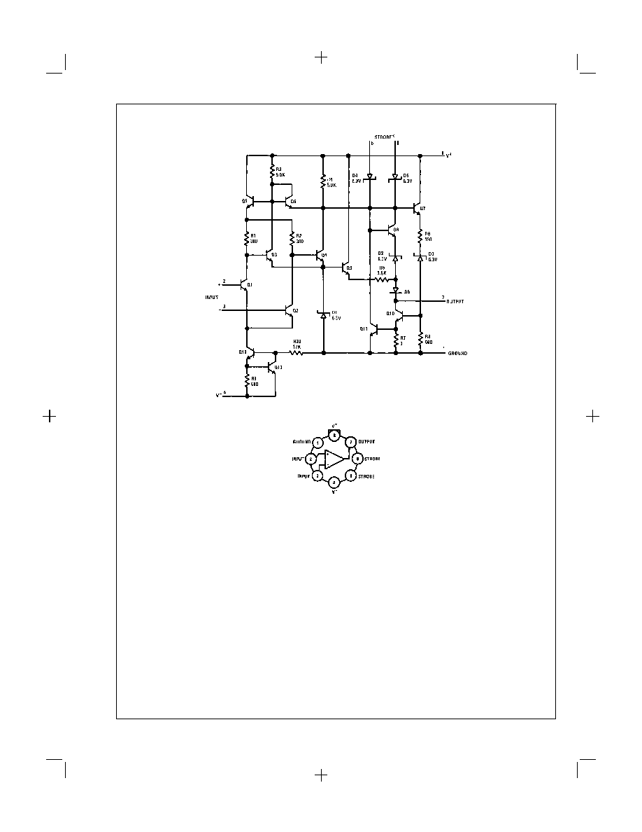
Schematic and Connection Diagrams
DS007756-1
Metal Can
DS007756-2
Note: Pin 4 connected to case.
Available per SMD# 8003701
Top View
Order Number LM106H,
LM106H/883
or LM306H
See NS Package Number H08A
PrintDate=1997/05/07 PrintTime=10:34:17 6917 ds007756 Rev. No. 1
Proof
2
www.national.com
2
Absolute Maximum Ratings
(Note *NO
TARGET FOR FNXref NS0058*)
If Military/Aerospace specified devices are required,
please contact the National Semiconductor Sales Office/
Distributors for availability and specifications.
(Note 6)
Positive Supply Voltage
15V
Negative Supply Voltage
-15V
Output Voltage
24V
Output to Negative Supply Voltage
30V
Differential Input Voltage
±
5V
Input Voltage
±
7V
Power Dissipation (Note 1)
600 mW
Output Short Circuit Duration
10 seconds
Operating Temperature Range
T
MIN
T
MAX
LM106
-55∞C to +125∞C
LM306
0∞C to +70∞C
Storage Temperature Range
-65∞C to +150∞C
Lead Temperature (Soldering, 10 sec.)
300∞C
ESD rating to be determined.
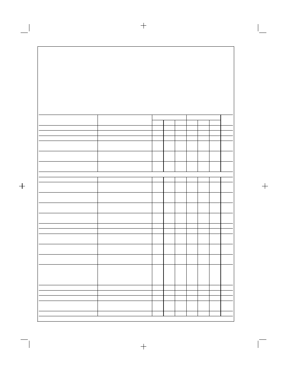
Electrical Characteristics
(Note 2)
Parameter
Conditions
LM106
LM306
Units
Min
Typ
Max
Min
Typ
Max
Input Offset Voltage
(Note 3)
0.5
2.0
1.6
5.0
mV
Input Offset Current
(Note 3)
0.7
3.0
1.8
5.0
µA
Input Bias Current
10
20
16
25
µA
Response Time
R
L
= 390
to 5V
28
40
28
40
ns
C
L
= 15 pF, (Note 4)
Saturation Voltage
V
IN
-5 mV, I
OUT
= 100 mA
1.0
1.5
V
V
IN
-7 mV, I
OUT
= 100 mA
0.8
2.0
V
Output Leakage Current
V
IN
5 mV, 8V
V
OUT
24V
0.02
1.0
µA
V
IN
7 mV, 8V
V
OUT
24V
0.02
2.0
µA
THE FOLLOWING SPECIFICATIONS APPLY FOR T
MIN
T
A
T
MAX
(Note 5)
Input Offset Voltage
(Note 3)
3.0
6.5
mV
Average Temperature Coefficient of
3.0
10
5
20
µV/∞C
Input Offset Voltage
Input Offset Current
T
L
T
A
25∞C, (Note 3)
1.8
7.0
2.4
7.5
µA
25∞C
T
A
T
H
0.25
3.0
5.0
µA
Average Temperature Coefficient of
25∞C
T
A
T
H
5.0
25
15
50
nA/∞C
Input Offset Current
T
L
T
A
25∞C
15
75
24
100
nA/∞C
Input Bias Current
T
L
T
A
25∞C
45
25
40
µA
25∞C
T
A
T
H
20
25
µA
Input Voltage Range
-7V
V
-
-12V
±
5.0
±
5.0
V
Differential Input Voltage Range
±
5.0
±
5.0
V
Saturation Voltage
V
IN
-5 mV, I
OUT
= 50 mA
1.0
1.0
V
V
IN
-8 mV For LM306
Saturation Voltage
V
IN
-5 mV, I
OUT
= 16 mA
0.4
0.4
V
V
IN
-8 mV For LM306
Positive Output Level
V
IN
5 mV, I
OUT
= -400µA
2.5
5.5
2.5
5.5
V
V
IN
8 mV For LM306
Output Leakage Current
V
IN
5 mV, 8V
V
OUT
24V
1.0
2.0
µA
V
IN
8 mV For LM306
T
L
T
A
25∞C
25∞C
<
T
A
T
H
100
100
µA
Strobe Current
V
STROBE
= 0.4V
-1.7
-3.2
-1.7
-3.2
mA
Strobe "ON" Voltage
0.9
1.4
0.9
1.4
V
Strobe "OFF" Voltage
I
SINK
16 mA
1.4
2.2
1.4
2.2
V
Positive Supply Current
V
IN
= -5 mV
5.5
10
5.5
10
mA
V
IN
= -8 mV for LM306
Negative Supply Current
-1.5
-3.6
-1.5
-3.6
mA
3
www.national.com
PrintDate=1997/05/07 PrintTime=10:34:19 6917 ds007756 Rev. No. 1
Proof
3
Electrical Characteristics
(Note 2) (Continued)
Note 1: The maximum junction temperature of LM106 is 150∞C, LM306 is 85∞C. For operating at elevated temperatures, devices must be derated based on a thermal
resistance of 170∞C/W, junction to ambient, or 23∞C/W, junction to case.
Note 2: These specifications apply for -3V
V
-
-12V, V
+
= 12V and T
A
= 25∞C unless otherwise specified. All currents into device pins are considered positive.
Note 3: The offset voltages and offset currents given are the maximum values required to drive the output down to 0.5V or up to 4.4V (0.5V or up to 4.8V for the
LM306). Thus, these parameters actually define an error band and take into account the worst-case effects of voltage gain, specified supply voltage variations, and
common mode voltage variations.
Note 4: The response time specified (see definitions) is for a 100 mV input step with 5 mV overdrive.
Note 5: All currents into device pins are considered positive.
Note 6: Refer to RETS106X for LM106 military specifications.
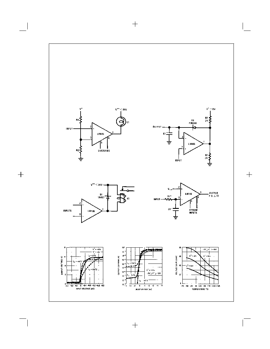
Typical Applications
Typical Performance Characteristics
Level Detector and Lamp Driver
DS007756-4
Fast Response Peak Detector
DS007756-5
Relay Driver
DS007756-6
Adjustable Threshold Line Receiver
DS007756-7
*Optional for response time control.
Transfer Function
DS007756-9
Transconductance
DS007756-10
Voltage Gain
DS007756-11
PrintDate=1997/05/07 PrintTime=10:34:20 6917 ds007756 Rev. No. 1
Proof
4
www.national.com
4
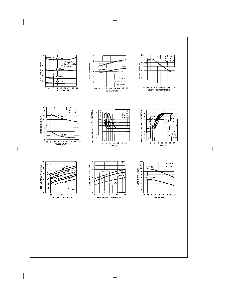
Typical Performance Characteristics
(Continued)
Saturation Voltage
DS007756-12
Positive Output Level
DS007756-13
Short Circuit Output Current
DS007756-14
Input Current
DS007756-15
Response Time for
Various Input Overdrives
DS007756-16
Response Time for
Various Input Overdrives
DS007756-17
Positive Supply Current
DS007756-18
Negative Supply Current
DS007756-19
Power Consumption
DS007756-20
5
www.national.com
PrintDate=1997/05/07 PrintTime=10:34:21 6917 ds007756 Rev. No. 1
Proof
5
Book
Extract
End