LM109/LM309
5-Volt Regulator
General Description
The LM109 series are complete 5V regulators fabricated on
a single silicon chip. They are designed for local regulation
on digital logic cards, eliminating the distribution problems
association with single-point regulation. The devices are
available in two standard transistor packages. In the
solid-kovar TO-5 header, it can deliver output currents in ex-
cess of 200 mA, if adequate heat sinking is provided. With
the TO-3 power package, the available output current is
greater than 1A.
The regulators are essentially blowout proof. Current limiting
is included to limit the peak output current to a safe value. In
addition, thermal shutdown is provided to keep the IC from
overheating. If internal dissipation becomes too great, the
regulator will shut down to prevent excessive heating.
Considerable effort was expended to make these devices
easy to use and to minimize the number of external compo-
nents. It is not necessary to bypass the output, although this
does improve transient response somewhat. Input bypass-
ing is needed, however, if the regulator is located very far
from the filter capacitor of the power supply. Stability is also
achieved by methods that provide very good rejection of load
or line transients as are usually seen with TTL logic.
Although designed primarily as a fixed-voltage regulator, the
output of the LM109 series can be set to voltages above 5V,
as shown. It is also possible to use the circuits as the control
element in precision regulators, taking advantage of the
good current-handling capability and the thermal overload
protection.
Features
n
Specified to be compatible, worst case, with TTL and
DTL
n
Output current in excess of 1A
n
Internal thermal overload protection
n
No external components required
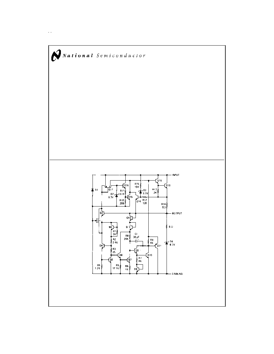
Schematic Diagram
DS007138-1
April 1998
LM109/LM309
5-V
olt
Regulator
� 1999 National Semiconductor Corporation
DS007138
www.national.com

Absolute Maximum Ratings
(Note 1)
If Military/Aerospace specified devices are required,
please contact the National Semiconductor Sales Office/
Distributors for availability and specifications.
Input Voltage
35V
Power Dissipation
Internally Limited
Operating Junction Temperature Range
LM109
-55�C to +150�C
LM309
0�C to +125�C
Storage Temperature Range
-65�C to +150�C
Lead Temperature
(Soldering, 10 sec.)
300�C
Electrical Characteristics
(Note 2)
Parameter
Conditions
LM109
LM309
Units
Min
Typ
Max
Min
Typ
Max
Output Voltage
T
j
= 25�C
4.7
5.05
5.3
4.8
5.05
5.2
V
Line Regulation
T
j
= 25�C
4.0
50
4.0
50
mV
7.10V
V
IN
25V
Load Regulation
T
j
= 25�C
TO-39 Package
5 mA
I
OUT
0.5A
15
50
15
50
mV
TO-3 Package
5 mA
I
OUT
1.5A
15
100
15
100
mV
Output Voltage
7.40V
V
IN
25V,
4.6
5.4
4.75
5.25
V
5 mA
I
OUT
I
MAX
,
P
<
P
MAX
Quiescent Current
7.40V
V
IN
25V
5.2
10
5.2
10
mA
Quiescent Current Change
7.40V
V
IN
25V
0.5
0.5
mA
5 mA
I
OUT
I
MAX
0.8
0.8
mA
Output Noise Voltage
T
A
= 25�C
40
40
�V
10 Hz
f
100 kHz
Long Term Stability
10
20
mV
Ripple Rejection
T
j
= 25�C
50
50
dB
Thermal Resistance,
(Note 3)
Junction to Case
TO-39 Package
15
15
�C/W
TO-3 Package
2.5
2.5
�C/W
Note 1: "Absolute Maximum Ratings" indicate limits beyond which damage to the device may occur. Operating Ratings indicate conditions for which the device is
functional, but do not guarantee specific performance limits.
Note 2: Unless otherwise specified, these specifications apply -55�C
T
j
+150�C for the LM109 and 0�C
T
j
+125�C for the LM309; V
IN
= 10V; and I
OUT
= 0.1A
for the TO-39 package or I
OUT
= 0.5A for the TO-3 package. For the TO-39 package, I
MAX
= 0.2A and P
MAX
= 2.0W. For the TO-3 package, I
MAX
= 1.0A and P
MAX
= 20W.
Note 3: Without a heat sink, the thermal resistance of the TO-39 package is about 150�C/W, while that of the TO-3 package is approximately 35�C/W. With a heat
sink, the effective thermal resistance can only approach the values specified, depending on the efficiency of the sink.
Note 4: Refer to RETS109H drawing for LM109H or RETS109K drawing for LM109K military specifications.
Connection Diagrams
Metal Can Packages
DS007138-33
Order Number LM109H, LM109H/883 or LM309H
See NS Package Number H03A
DS007138-34
Order Number LM109K STEEL or
LM309K STEEL
See NS Package Number K02A
Order Number LM109K/883
See NS Package Number K02C
www.national.com
2
Application Hints
1.
Bypass the input of the LM109 to ground with
0.2 �F
ceramic or solid tantalum capacitor if main filter capaci-
tor is more than 4 inches away.
2.
Avoid insertion of regulator into "live" socket if input
voltage is greater than 10V. The output will rise to within
2V of the unregulated input if the ground pin does not
make contact, possibly damaging the load. The LM109
may also be damaged if a large output capacitor is
charged up, then discharged through the internal clamp
zener when the ground pin makes contact.
3.
The output clamp zener is designed to absorb tran-
sients only. It will not clamp the output effectively if a fail-
ure occurs in the internal power transistor structure. Ze-
ner dynamic impedance is
4
. Continuous RMS
current into the zener should not exceed 0.5A.
4.
Paralleling of LM109s for higher output current is not
recommended. Current sharing will be almost nonexist-
ent, leading to a current limit mode operation for devices
with the highest initial output voltage. The current limit
devices may also heat up to the thermal shutdown point
(
175�C). Long term reliability cannot be guaranteed
under these conditions.
5.
Preventing latchoff for loads connected to negative
voltage:
If the output of the LM109 is pulled negative by a high cur-
rent supply so that the output pin is more than 0.5V negative
with respect to the ground pin, the LM109 can latch off. This
can be prevented by clamping the ground pin to the output
pin with a germanium or Schottky diode as shown. A silicon
diode (1N4001) at the output is also needed to keep the
positive output from being pulled too far negative. The 10
resistor will raise +V
OUT
by
0.05V.
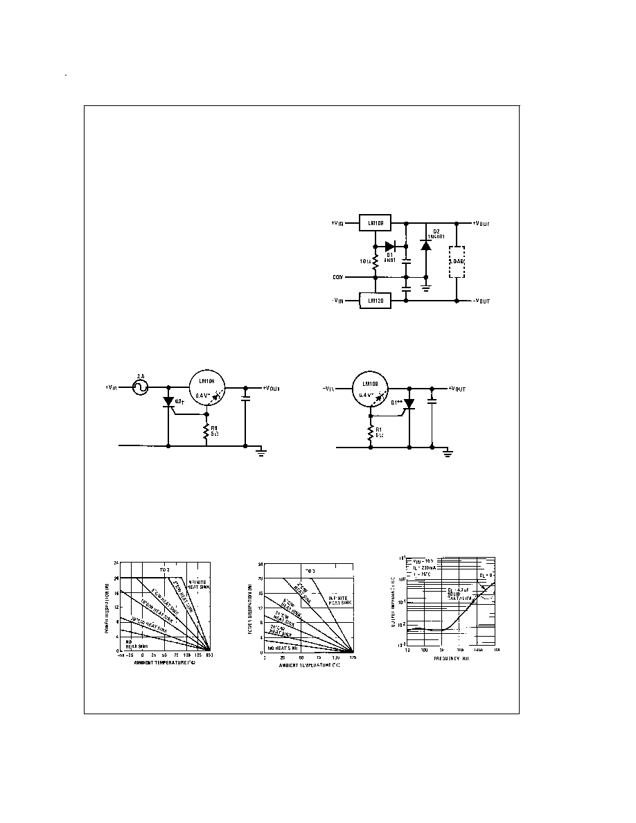
Crowbar Overvoltage Protection
Typical Performance Characteristics
DS007138-7
Input Crowbar
DS007138-8
Output Crowbar
DS007138-9
*Zener is internal to LM109.
*
*
Q1 must be able to withstand 7A continuous current if fusing is not used
at regulator input. LM109 bond wires will fuse at currents above 7A.
Q2 is selected for surge capability. Consideration must be given to filter
capacitor size, transformer impedance, and fuse blowing time.
Trip point is
7.5V.
Maximum Average
Power Dissipation (LM109K)
DS007138-16
Maximum Average
Power Dissipation (LM309K)
DS007138-17
Output Impedance
DS007138-18
www.national.com
3
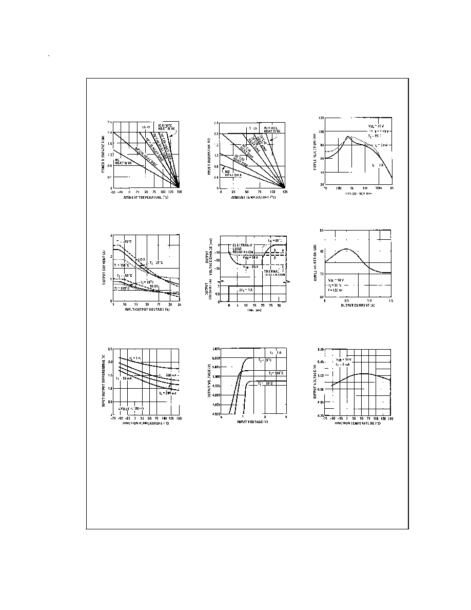
Typical Performance Characteristics
(Continued)
Maximum Average
Power Dissipation (LM109H)
DS007138-19
Maximum Average
Power Dissipation (LM309H)
DS007138-20
Ripple Rejection
DS007138-21
Current Limit
Characteristics (Note 5)
DS007138-22
Thermally Induced Output
Voltage Variation
DS007138-23
Ripple Rejection
DS007138-24
Note 5: Current limiting foldback characteristics are determined by input output differential, not by output voltage.
Input-Output Differential (V)
DS007138-25
Output Voltage (V)
DS007138-26
Output Voltage (V)
DS007138-27
www.national.com
4
Typical Performance Characteristics
(Continued)
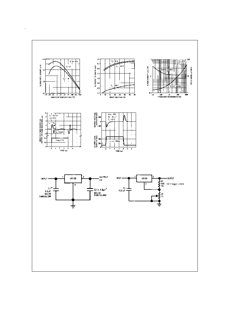
Typical Applications
Quiescent Current
DS007138-28
Quiescent Current
DS007138-29
Output Voltage Noise
DS007138-30
Line Transient Response
DS007138-31
Load Transient Response
DS007138-32
Fixed 5V Regulator
DS007138-2
*Required if regulator is located more than 4" from power supply filter
capacitor.
Although no output capacitor is needed for stability, it does improve
transient response.
C2 should be used whenever long wires are used to connect to the load,
or when transient response is critical.
Note: Pin 3 electrically connected to case.
Adjustable Output Regulator
DS007138-4
www.national.com
5