TL H 7751
LM112LM212LM312
Operational
Amplifiers
September 1992
LM112 LM212 LM312 Operational Amplifiers
General Description
The LM112 series are micropower operational amplifiers
with very low offset-voltage and input-current errors
at
least a factor of ten better than FET amplifiers over a
b
55 C to
a
125 C temperature range Similar to the LM108
series that also use supergain transistors they differ in that
they include internal frequency compensation and have pro-
visions for offset adjustment with a single potentiometer
These amplifiers will operate on supply voltages of
g
2V to
g
20V drawing a quiescent current of only 300 mA Per-
formance is not appreciably affected over this range of volt-
ages so operation from unregulated power sources is easily
accomplished They can also be run from a single supply
like the 5V used for digital circuits
The LM112 series are the first IC amplifiers to improve reli-
ability by including overvoltage protection for the MOS com-
pensation capacitor Without this feature IC's have been
known to suffer catastrophic failure caused by short-dura-
tion overvoltage spikes on the supplies Unlike other inter-
nally-compensated IC amplifiers it is possible to overcom-
pensate with an external capacitor to increase stability mar-
gin
The LM212 is identical to the LM112 except that the LM212
has its performance guaranteed over a
b
25 C to
a
85 C
temperature range instead of
b
55 C to
a
125 C The
LM312 is guaranteed over a 0 C to
a
70 C temperature
range
Features
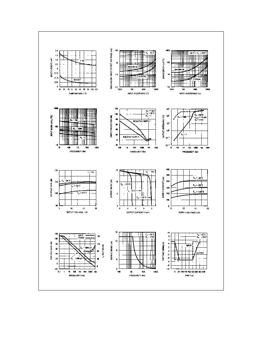
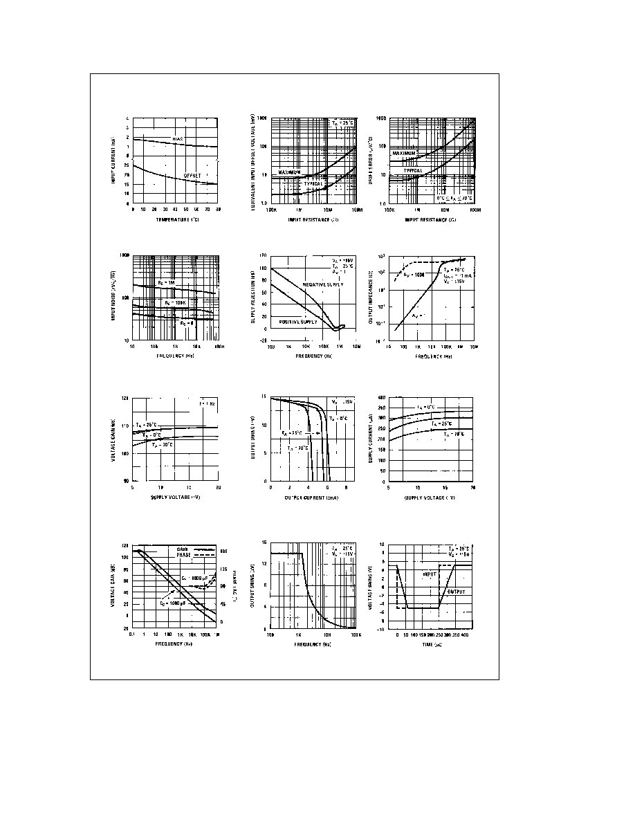
Y
Maximum input bias current of 3 nA over temperature
Y
Offset current less than 400 pA over temperature
Y
Low noise
Y
Guaranteed drift specifications
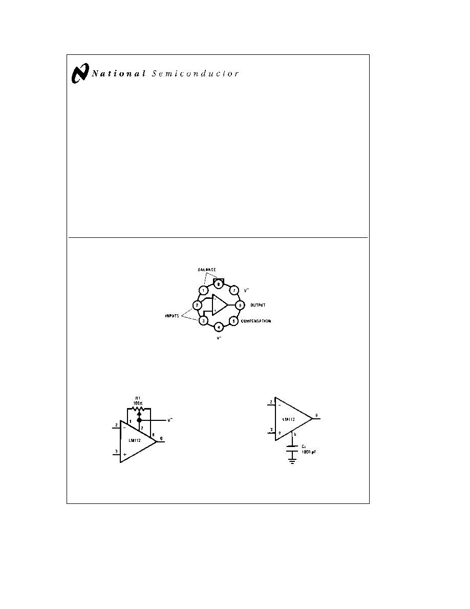
Connection Diagram
Metal Can Package
TL H 7751 ≠ 4
Top View
Order Number LM112H LM212H LM312H or LM112H 883
See NS Package Number H08C
Auxiliary Circuits
Offset Balancing
TL H 7751 ≠ 2
Overcompensation for Greater Stability Margin
TL H 7751 ≠ 3
C1995 National Semiconductor Corporation
RRD-B30M115 Printed in U S A
Absolute Maximum Ratings
If Military Aerospace specified devices are required please contact the
National
Semiconductor
Sales
Office Distributors
for
availability
and
specifications
(Note 5)
LM112 LM212
LM312
Supply Voltage
g
20V
g
18V
Power Dissipation (Note 1)
500 mW
500 mW
Differential Input Current (Note 2)
g
10 mA
g
10 mA
Input Voltage (Note 3)
g
15V
g
15V
Output Short-Circuit Duration
Continuous
Continuous
Operating Temperature Range
LM112
b
55 C to
a
125 C
0 C to
a
70 C
LM212
b
25 C to
a
85 C
Storage Temperature Range
b
65 C to
a
150 C
b
65 C to
a
150 C
Lead Temperature (Soldering 10 sec )
300 C
300 C
ESD rating to be determined
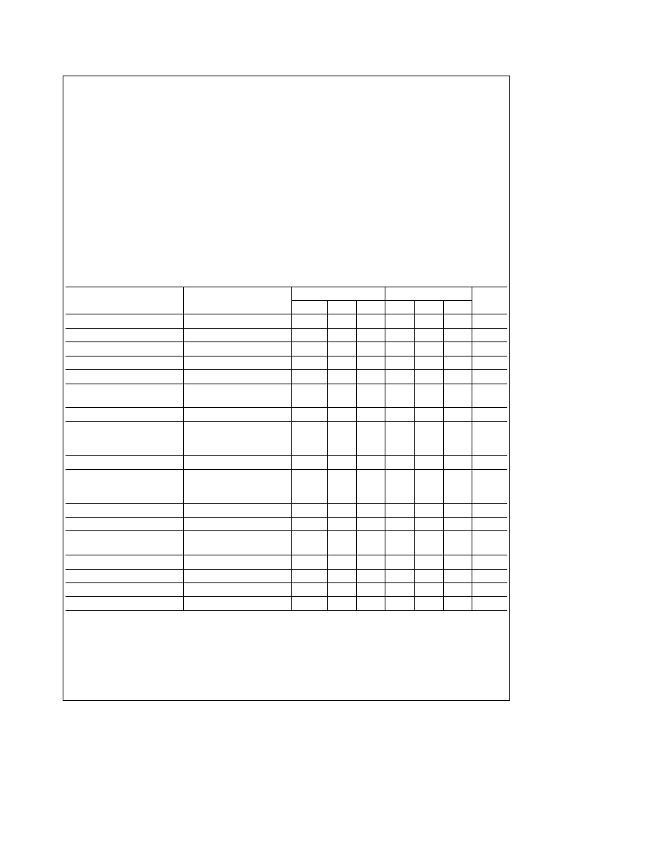
Electrical Characteristics
(Note 4)
Parameter
Conditions
LM112 LM212
LM312
Units
Min
Typ
Max
Min
Typ
Max
Input Offset Voltage
T
A
e
25 C
0 7
2 0
2 0
7 5
mV
Input Offset Current
T
A
e
25 C
0 05
0 2
0 2
1
nA
Input Bias Current
T
A
e
25 C
0 8
2 0
1 5
7
nA
Input Resistance
T
A
e
25 C
30
70
10
40
MX
Supply Current
T
A
e
25 C
0 3
0 6
0 3
0 8
mA
Large Signal Voltage Gain
T
A
e
25 C V
S
e
g
15V
50
300
25
300
V mV
V
OUT
e
g
10V R
L
t
10 kX
Input Offset Voltage
3 0
10
mV
Average Temperature
Coefficient of Input
3 0
15
6 0
30
m
V C
Offset Voltage
Input Offset Current
0 4
1 5
nA
Average Temperature
Coefficient of Input
0 5
2 5
2 0
10
pA C
Offset Current
Input Bias Current
3 0
10
nA
Supply Current
T
A
e
125 C
0 15
0 4
mA
Large Signal Voltage Gain
V
S
e
g
15V V
OUT
e
g
10V
R
L
t
10 kX
25
15
V mV
Output Voltage Swing
V
S
e
g
15V R
L
e
10 kX
g
13
g
14
g
13
g
14
V
Input Voltage Range
V
S
e
g
15V
g
13 5
g
14
V
Common-Mode Rejection Ratio
85
100
80
100
dB
Supply Voltage Rejection Ratio
80
96
80
96
dB
Note 1
The maximum junction temperature of the LM112 is 150 C LM212 is 100 C and LM312 is 85 C For operating at elevated temperatures devices in the H08
package must be derated based on a thermal resistance of 160 C W junction to ambient or 20 C W junction to case
Note 2
The inputs are shunted with shunt diodes for overvoltage protection Therefore excessive current will flow if a differential input voltage in excess of 1V is
applied between the inputs unless some limiting resistance is used
Note 3
For supply voltages less than
g
15V the absolute maximum input voltage is equal to the supply voltage
Note 4
These specifications apply for
g
5V
s
V
S
s
g
20V and
b
55 C
s
T
A
s
a
125 C (LM112)
b
25 C
s
T
A
s
a
85 C (LM212)
g
5V
s
V
S
s
g
15V and
0 C
s
T
A
s a
70 C (LM312) unless otherwise noted
Note 5
Refer to RETS112X for LM112H military specifications
2