LM117/LM317A/LM317
3-Terminal Adjustable Regulator
General Description
The LM117 series of adjustable 3-terminal positive voltage
regulators is capable of supplying in excess of 1.5A over a
1.2V to 37V output range. They are exceptionally easy to
use and require only two external resistors to set the output
voltage. Further, both line and load regulation are better than
standard fixed regulators. Also, the LM117 is packaged in
standard transistor packages which are easily mounted and
handled.
In addition to higher performance than fixed regulators, the
LM117 series offers full overload protection available only in
IC's. Included on the chip are current limit, thermal overload
protection and safe area protection. All overload protection
circuitry remains fully functional even if the adjustment ter-
minal is disconnected.
Normally, no capacitors are needed unless the device is
situated more than 6 inches from the input filter capacitors in
which case an input bypass is needed. An optional output
capacitor can be added to improve transient response. The
adjustment terminal can be bypassed to achieve very high
ripple rejection ratios which are difficult to achieve with stan-
dard 3-terminal regulators.
Besides replacing fixed regulators, the LM117 is useful in a
wide variety of other applications. Since the regulator is
"floating" and sees only the input-to-output differential volt-
age, supplies of several hundred volts can be regulated as
long as the maximum input to output differential is not ex-
ceeded, i.e., avoid short-circuiting the output.
Also, it makes an especially simple adjustable switching
regulator, a programmable output regulator, or by connecting
a fixed resistor between the adjustment pin and output, the
LM117 can be used as a precision current regulator. Sup-
plies with electronic shutdown can be achieved by clamping
the adjustment terminal to ground which programs the out-
put to 1.2V where most loads draw little current.
For applications requiring greater output current, see LM150
series (3A) and LM138 series (5A) data sheets. For the
negative complement, see LM137 series data sheet.
Features
n
Guaranteed 1% output voltage tolerance (LM317A)
n
Guaranteed max. 0.01%/V line regulation (LM317A)
n
Guaranteed max. 0.3% load regulation (LM117)
n
Guaranteed 1.5A output current
n
Adjustable output down to 1.2V
n
Current limit constant with temperature
n
P
+
Product Enhancement tested
n
80 dB ripple rejection
n
Output is short-circuit protected
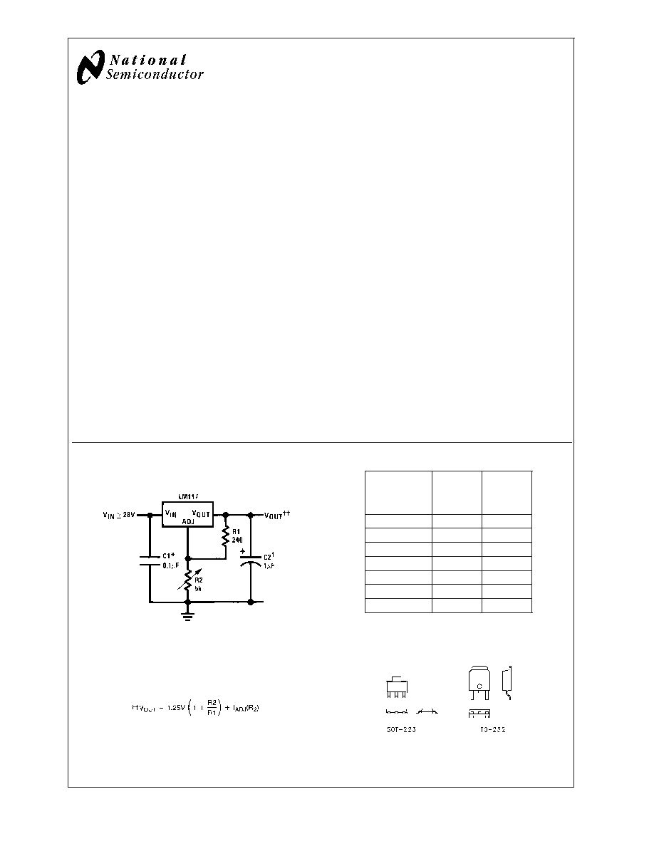
Typical Applications
1.2V≠25V Adjustable Regulator
00906301
Full output current not available at high input-output voltages
*Needed if device is more than 6 inches from filter capacitors.
Optional -- improves transient response. Output capacitors in the range
of 1µF to 1000µF of aluminum or tantalum electrolytic are commonly used
to provide improved output impedance and rejection of transients.
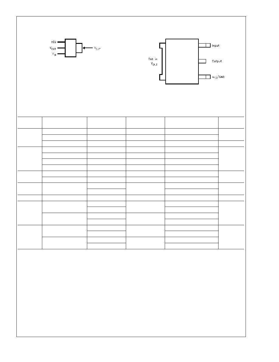
LM117 Series Packages
Part Number
Design
Suffix
Package
Load
Current
K
TO-3
1.5A
H
TO-39
0.5A
T
TO-220
1.5A
E
LCC
0.5A
S
TO-263
1.5A
EMP
SOT-223
1A
MDT
TO-252
0.5A
SOT-223 vs. D-Pak (TO-252)
Packages
00906354
Scale 1:1
May 2003
LM1
17/LM317A/LM317
3-T
erminal
Adjustable
Regulator
© 2003 National Semiconductor Corporation
DS009063
www.national.com
Absolute Maximum Ratings
(Note 1)
If Military/Aerospace specified devices are required,
please contact the National Semiconductor Sales Office/
Distributors for availability and specifications.
Power Dissipation
Internally Limited
Input-Output Voltage Differential
+40V, -0.3V
Storage Temperature
-65∞C to +150∞C
Lead Temperature
Metal Package (Soldering, 10 seconds)
300∞C
Plastic Package (Soldering, 4 seconds)
260∞C
ESD Tolerance (Note 5)
3 kV
Operating Temperature Range
LM117
-55∞C
T
J
+150∞C
LM317A
-40∞C
T
J
+125∞C
LM317
0∞C
T
J
+125∞C
Preconditioning
Thermal Limit Burn-In
All Devices 100%
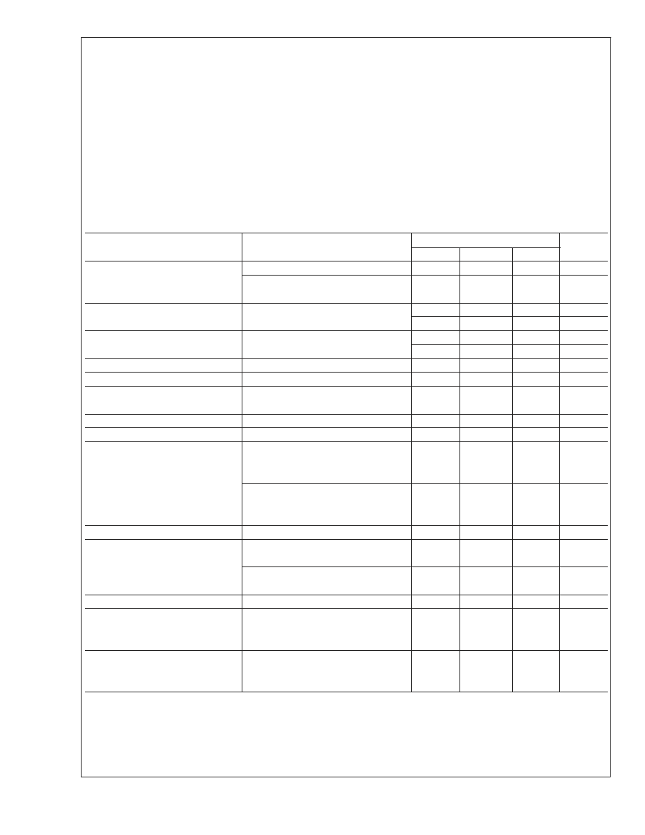
Electrical Characteristics
(Note 3)
Specifications with standard type face are for T
J
= 25∞C, and those with boldface type apply over full Operating Tempera-
ture Range. Unless otherwise specified, V
IN
- V
OUT
= 5V, and I
OUT
= 10 mA.
Parameter
Conditions
LM117 (Note 2)
Units
Min
Typ
Max
Reference Voltage
V
3V
(V
IN
- V
OUT
)
40V,
1.20
1.25
1.30
V
10 mA
I
OUT
I
MAX
, P
P
MAX
Line Regulation
3V
(V
IN
- V
OUT
)
40V (Note 4)
0.01
0.02
%/V
0.02
0.05
%/V
Load Regulation
10 mA
I
OUT
I
MAX
(Note 4)
0.1
0.3
%
0.3
1
%
Thermal Regulation
20 ms Pulse
0.03
0.07
%/W
Adjustment Pin Current
50
100
µA
Adjustment Pin Current Change
10 mA
I
OUT
I
MAX
0.2
5
µA
3V
(V
IN
- V
OUT
)
40V
Temperature Stability
T
MIN
T
J
T
MAX
1
%
Minimum Load Current
(V
IN
- V
OUT
) = 40V
3.5
5
mA
Current Limit
(V
IN
- V
OUT
)
15V
K Package
1.5
2.2
3.4
A
H Package
0.5
0.8
1.8
A
(V
IN
- V
OUT
) = 40V
K Package
0.3
0.4
A
H Package
0.15
0.2
A
RMS Output Noise, % of V
OUT
10 Hz
f 10 kHz
0.003
%
Ripple Rejection Ratio
V
OUT
= 10V, f = 120 Hz,
65
dB
C
ADJ
= 0 µF
V
OUT
= 10V, f = 120 Hz,
66
80
dB
C
ADJ
= 10 µF
Long-Term Stability
T
J
= 125∞C, 1000 hrs
0.3
1
%
Thermal Resistance,
K Package
2.3
3
∞C/W
Junction-to-Case
H Package
12
15
∞C/W
E Package
∞C/W
Thermal Resistance, Junction-
K Package
35
∞C/W
to-Ambient (No Heat Sink)
H Package
140
∞C/W
E Package
∞C/W
LM1
17/LM317A/LM317
www.national.com
4
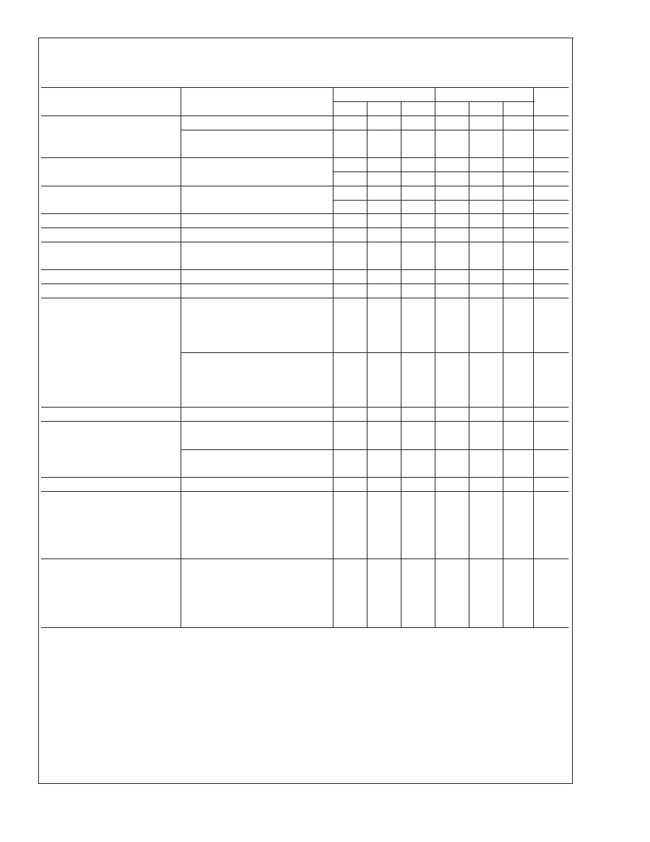
Electrical Characteristics
(Note 3)
Specifications with standard type face are for T
J
= 25∞C, and those with boldface type apply over full Operating Tempera-
ture Range. Unless otherwise specified, V
IN
- V
OUT
= 5V, and I
OUT
= 10 mA.
Parameter
Conditions
LM317A
LM317
Units
Min
Typ
Max
Min
Typ
Max
Reference Voltage
1.238
1.250
1.262
V
3V
(V
IN
- V
OUT
)
40V,
1.225
1.250
1.270
1.20
1.25
1.30
V
10 mA
I
OUT
I
MAX
, P
P
MAX
Line Regulation
3V
(V
IN
- V
OUT
)
40V (Note 4)
0.005
0.01
0.01
0.04
%/V
0.01
0.02
0.02
0.07
%/V
Load Regulation
10 mA
I
OUT
I
MAX
(Note 4)
0.1
0.5
0.1
0.5
%
0.3
1
0.3
1.5
%
Thermal Regulation
20 ms Pulse
0.04
0.07
0.04
0.07
%/W
Adjustment Pin Current
50
100
50
100
µA
Adjustment Pin Current
Change
10 mA
I
OUT
I
MAX
0.2
5
0.2
5
µA
3V
(V
IN
- V
OUT
)
40V
Temperature Stability
T
MIN
T
J
T
MAX
1
1
%
Minimum Load Current
(V
IN
- V
OUT
) = 40V
3.5
10
3.5
10
mA
Current Limit
(V
IN
- V
OUT
)
15V
K, T, S Packages
1.5
2.2
3.4
1.5
2.2
3.4
A
H Package
MP Package
0.5
1.5
0.8
2.2
1.8
3.4
0.5
1.5
0.8
2.2
1.8
3.4
A
A
(V
IN
- V
OUT
) = 40V
K, T, S Packages
0.15
0.4
0.15
0.4
A
H Package
MP Package
0.075
0.55
0.2
0.4
0.075
0.15
0.2
0.4
A
A
RMS Output Noise, % of V
OUT
10 Hz
f 10 kHz
0.003
0.003
%
Ripple Rejection Ratio
V
OUT
= 10V, f = 120 Hz,
65
65
dB
C
ADJ
= 0 µF
V
OUT
= 10V, f = 120 Hz,
66
80
66
80
dB
C
ADJ
= 10 µF
Long-Term Stability
T
J
= 125∞C, 1000 hrs
0.3
1
0.3
1
%
Thermal Resistance,
Junction-to-Case
K Package
MDT Package
2.3
5
3
∞C/W
∞C/W
H Package
12
15
12
15
∞C/W
T Package
MP Package
4
23.5
5
4
23.5
∞C/W
∞C/W
Thermal Resistance,
Junction-to-Ambient (No Heat
Sink)
K Package
MDT Package(Note 6)
35
35
92
∞C/W
∞C/W
H Package
140
140
∞C/W
T Package
50
50
∞C/W
S Package (Note 6)
50
50
∞C/W
Note 1: Absolute Maximum Ratings indicate limits beyond which damage to the device may occur. Operating Ratings indicate conditions for which the device is
intended to be functional, but do not guarantee specific performance limits. For guaranteed specifications and test conditions, see the Electrical Characteristics. The
guaranteed specifications apply only for the test conditions listed.
Note 2: Refer to RETS117H drawing for the LM117H, or the RETS117K for the LM117K military specifications.
Note 3: Although power dissipation is internally limited, these specifications are applicable for maximum power dissipations of 2W for the TO-39 and SOT-223 and
20W for the TO-3, TO-220, and TO-263. I
MAX
is 1.5A for the TO-3, TO-220, and TO-263 packages, 0.5A for the TO-39 package and 1A for the SOT-223 Package.
All limits (i.e., the numbers in the Min. and Max. columns) are guaranteed to National's AOQL (Average Outgoing Quality Level).
Note 4: Regulation is measured at a constant junction temperature, using pulse testing with a low duty cycle. Changes in output voltage due to heating effects are
covered under the specifications for thermal regulation.
Note 5: Human body model, 100 pF discharged through a 1.5 k
resistor.
Note 6: If the TO-263 or TO-252 packages are used, the thermal resistance can be reduced by increasing the PC board copper area thermally connected to the
package. Using 0.5 square inches of copper area.
JA
is 50∞C/W; with 1 square inch of copper area,
JA
is 37∞C/W; and with 1.6 or more square inches of copper
area,
JA
is 32∞C/W. If the SOT-223 package is used, the thermal resistance can be reduced by increasing the PC board copper area (see applications hints for
heatsinking).
LM1
17/LM317A/LM317
www.national.com
5