 | –≠–ª–µ–∫—Ç—Ä–æ–Ω–Ω—ã–π –∫–æ–º–ø–æ–Ω–µ–Ω—Ç: LM1204 | –°–∫–∞—á–∞—Ç—å:  PDF PDF  ZIP ZIP |
TL H 11238
LM1204
150
MHz
RGB
Video
Amplifier
System
December 1994
LM1204 150 MHz RGB Video Amplifier System
General Description
The LM1204 is a triple 150 MHz video amplifier system
designed specifically for high resolution RGB video display
applications In addition to three matched video amplifiers
the LM1204 contains a DC operated contrast control a DC
operated drive control for each amplifier and a dual clamp-
ing system for both brightness control and video blanking
The LM1204 also contains a back porch clamp pulse gener-
ator which is activated by an externally supplied
g
H HV
sync signal or by an external composite video signal The
g
H HV sync input will have priority over the composite vid-
eo input A single
b
H HV sync output is provided for the
automatically selected sync input signal The back porch
clamp pulse width is user adjustable from 0 3 ms to 4 ms
The LM1204 video output stage will directly drive most
Hybrid or discrete CRT amplfier input stages without the
need for an external buffer transistor The device has been
designed to operate from a 12V supply with all DC controls
operating over a 0V to 4V range providing for an easy inter-
face to serial digital buss controlled monitors
Features
Y
Built-in video blanking function
Y
Built-in sync separator for composite video input
Y
Includes DC restoration of video signals
Y
Back porch clamp pulse width user adjustable
Y
DC control of brightness contrast blanking level drive
and cutoff
Y
DC controls are 0V to 4V for easy interfacing to a
digitally controlled system
Key Specifications
Y
150 MHz large signal bandwidth (typ)
Y
2 3 ns rise fall times (typ)
Y
0 1 dB contrast tracking (typ)
Y
g
3 dB drive (D gain) adjustments on R G B channels
(typ)
Applications
Y
High resolution CRT monitors
Y
Video AGC amplifier
Y
Wideband amplifier with gain and DC offset control
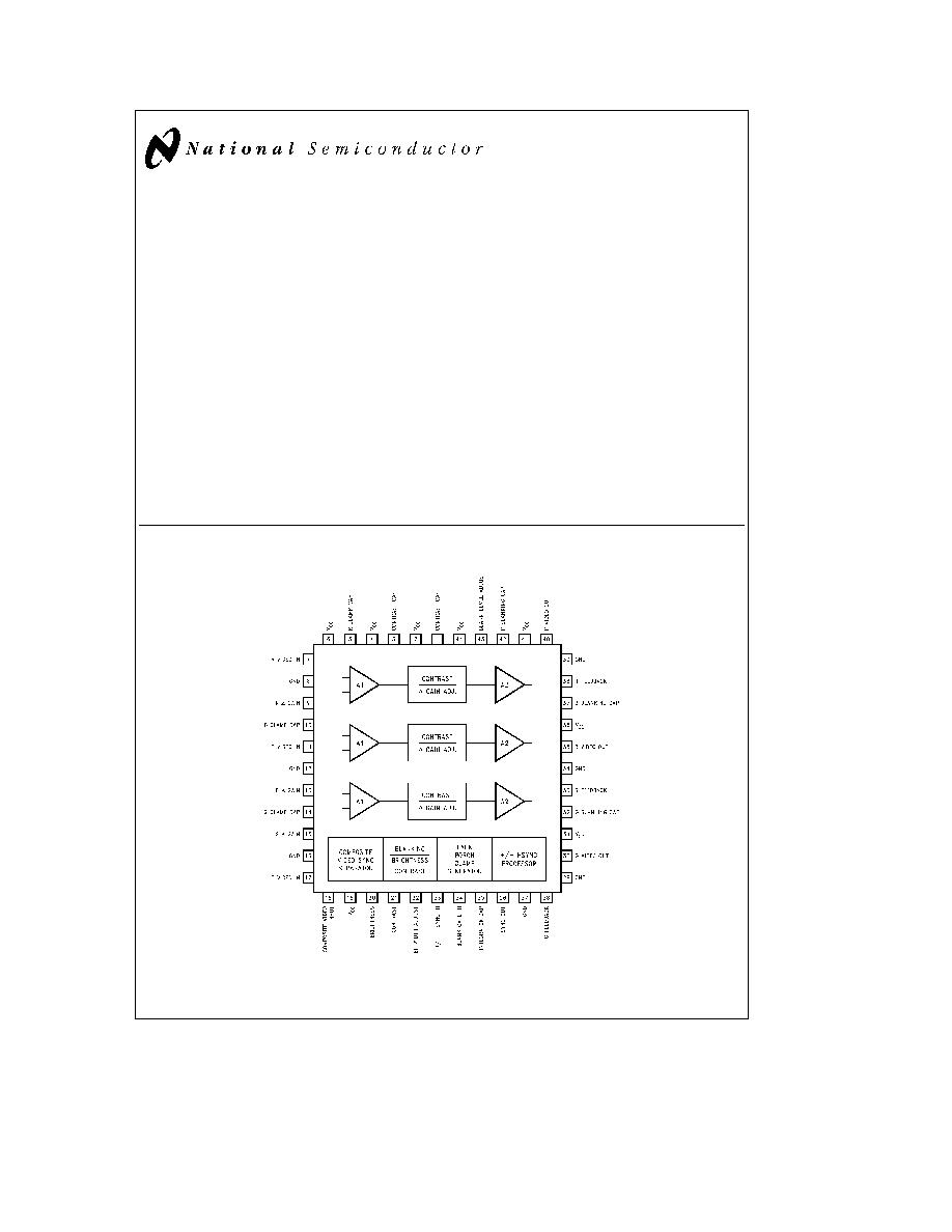
Block Diagram and Connection Diagram
Top View
TL H 11238 ≠ 1
Ordering Information
Order Number LM1204V
See NS Package Number V44A
C1995 National Semiconductor Corporation
RRD-B30M115 Printed in U S A

Absolute Maximum Ratings
(Note 1)
If Military Aerospace specified devices are required
please contact the National Semiconductor Sales
Office Distributors for availability and specifications
Supply Voltage V
CC
Pins 2 4 6 19 31 41 44 (Note 3)
13 5V
Peak Video Output Source Current
(Any One Amplifier) Pins 30 35 or 39
30 mA
Voltage at Any Input Pin V
IN
GND
s
V
IN
s
V
CC
Maximum
g
H Sync Input Voltage
5 5 V
PP
Power Dissipation PD (Above 25 C
Derate Based on i
JA
and T
J
)
2 4W
Thermal Resistance i
JA
52 C W
Junction Temperature T
J
150 C
ESD Susceptibility (Note 4)
2 5 kV
Storage Temperature
b
65 C to 150 C
Lead Temperature
Vapor Phase (60 seconds)
215 C
Infrared (15 seconds)
220 C
Operating Ratings
(Note 2)
Temperature Range
0 C to 70 C
Supply Voltage V
CC
10 8V
s
V
CC
s
13 2V
DC Electrical Characteristics (Video Amplifier Section)
The following specifications apply for V
CC
(pins 2 4 6 19 31 36 41 and 44)
e
12V and T
A
e
25 C unless otherwise specified
S1
e
B S2
e
B S3 4 5 closed V9 13 15
e
2V V20 21 22 24 43
e
0 5V unless otherwise specified see test circuit
Figure 1
Symbol
Parameter
Conditions
Typical
Limit
Units
(Note 5)
(Note 6)
I
S
Supply Current
No Video or Sync Input
100
125
mA
Signals S1
e
A
(Max)
I
B
Input Bias Current
S1
e
A
0 3
2
m
A
(Pin 9 13 15 20 21 or 22)
(Max)
I
24h
Blank Gate Input High Current
V24
e
4V
0 01
2
m
A
(Max)
I
24l
Blank Gate Input Low Current
V24
e
0V
2
5
m
A
(Max)
I
FB
Feedback Input Current
150
nA
(Pin 28 33 or 38)
I
Blanka
Blank Cap Charge Current
V
32 37 42
e
0V
185
75
m
A (Min)
I
Blankb
Blank Cap Discharge Current
V
32 37 42
e
5V
b
185
b
75
m
A (Min)
I
BB
Blank Cap Bias Current (Pins 32 37 42)
20
nA
I
Clampa
Clamp Cap Charge Current
V
5 10 14
e
0V
185
75
m
A (Min)
I
Clampb
Blank Cap Discharge Current
V
5 10 14
e
5V
b
185
b
75
m
A (Min)
I
CB
Clamp Cap Bias Current (Pins 5 10 14)
20
nA
V
24h
Blank Gate High Input Voltage
Input Signal is Not Blanked
2
V (Min)
V
24l
Blank Gate Low Input Voltage
Input Signal is Blanked
0 8
V (Max)
Blank Comparator Offset Voltage
Voltage between V43 and
2
50
mV
Any One Video Output
(Max)
V
H
Video Output High Voltage
R
L
e
350X
8 7
7
V(Min)
(Pins 30 35 40)
V28 33 38
e
0V
V
L
Video Output Low Voltage
R
L
e
350X
0 1
0 5
V(Max)
(Pins 30 35 40)
V28 33 38
e
4V
V
CM43
Common Mode Range of Blank
0 5
V(Min)
Comparator (Pins 43 28 33 38)
4
V(Max)
2
DC Electrical Characteristics (Sync Separator Processor Section)
The following specifications apply for V
CC
(Pins 2 4 6 19 31 36 41 and 44)
e
12V and T
A
e
25 C unless otherwise
specified S1
e
B S2
e
B S3 4 5 closed V9 13 15
e
2V V20 21 22 24 43
e
0 5V unless otherwise specified see Test
Circuit
Figure 1
Symbol
Parameter
Conditions
Typical
Limit
Units
(Note 5)
(Note 6)
b
H V
OH
b
H Sync Output Logic High (Pin 26)
4 2
2 4
V(Min)
b
H V
OL
b
H Sync Output Logic Low (Pin 26)
0 1
0 4
V(Max)
V
23
Quiescent DC Voltage at
g
H
3
V
Sync Input
AC Electrical Characteristics (Video Amplifier Section)
The following specifications apply for V
CC
(Pins 2 4 6 19 31 36 41 and 44)
e
12V and T
A
e
25 C unless otherwise
specified S1
e
B S2
e
B S3 4 5 closed V9 13 15 21 24 43
e
4V V20
e
2V unless otherwise specified see Test Circuit
Figure 1
Symbol
Parameter
Conditions
Typical
Limit
Units
(Note 5)
(Note 6)
R
IN
Video Amplifier Input Resistance
20
kX
A
Vmax
Maximum Video Amplifier Gain
f
IN
e
12 kHz
10
5 5
V V(Min)
D
A
Vtrack
Amplifier Gain (Contrast)
0 1
dB
Tracking (Note 7)
D
A
V2V
Attenuation at 2V
Ref A
Vmax
V21
e
2V
6
dB
D
A
V0 5V
Attenuation at 0 5V
Ref A
Vmax
V21
e
0 5V
28
20
dB(Min)
D
Gain
D
Gain Range (Pins 9 13 15)
V9 13 15
e
0V to 4V
g
3
dB
D
V
O
Max Brightness Tracking Error (Note 8)
100
mV
f
b
3 dB
Video Amplifier Bandwidth (Note 9)
V
OUT
e
3 5 V
PP
150
MHz
THD
Video Amplifier Distortion
V
OUT
e
1 V
PP
f
e
12 kHz
0 3
%
t
R
Video Output Rise Time (Note 9)
Square Wave Input
2 0
ns
V
OUT
e
3 5 V
PP
R
L
e
350X
t
F
Video Output Fall Time (Note 9)
Square Wave Input
2 3
ns
V
OUT
e
3 5 V
PP
R
L
e
350X
V
ISO (1 MHz)
Video Amplifier 1 MHz
b
50
dB
Isolation (Notes 9 10)
V
ISO (130 MHz)
Video Amplifier 130 MHz
b
10
dB
Isolation (Notes 9 10)
3
AC Electrical Characteristics (Sync Separator Processor Section)
The following specifications apply for V
CC
(Pins 2 4 6 19 31 36 41 and 44)
e
12V and T
A
e
25 C unless otherwise
specified S1
e
A S2
e
B S3 4 5 closed V9 13 15 20 21 43
e
2V unless otherwise specified see Test Circuit
Figure 1
and Timing Diagram for input waveform
Symbol
Parameter
Conditions
Typical
Limit
Units
(Note 5)
(Note 6)
V
18(Min)
Composite Video Input Voltage
S2
e
A Input
e
10% Duty
0 15
V
PP
(Pin 18)
Cycle Test for Loss of BP
(Min)
V
18(Max)
Composite Video Input Voltage
Pulse at Pin 26
2
V
PP
(Pin 18)
(Max)
V
23
g
H Sync Input Voltage (Pin 23)
Input
e
10% Duty Cycle
1 6
V
PP
(Min)
Back Porch Clamp Pulse Width
S2
e
A Pin 26
e
BP Output
1
1 4
m
s
at V
24
e
1V
(Max)
Back Porch Clamp Pulse Width
300
600
ns
at V
24
e
4V
(Max)
Maximum
g
H Sync Input Frequency
600
KHz
D
HI
Max Duty Cycle of Active High
Test for Loss of Sync
22
%
H Sync (Pin 23)
at Pin 26
D
LO
Max Duty Cycle of Active Low
22
%
H Sync (Pin 23)
t
pdl1
g
H Sync Input to
b
H Sync
Input
e
10% Duty Cycle
100
ns
Output Low Delay
t
pdh1
g
H Sync Input to
b
H Sync
Input
e
10% Duty Cycle
65
ns
Output High Delay
t
pd1
g
H Sync Input Trailing Edge to
Input
e
10% Duty Cycle
70
ns
Back Porch Clamp Output Delay
S2
e
A
t
pdl2
Composite Video Input to
b
H
Input
e
10% Duty Cycle
106
ns
Sync Output Low Delay
t
pdh2
Composite Video Input to
b
H
Input
e
10% Duty Cycle
68
ns
Sync Output High Delay
t
pd2
Composite Video Input Trailing
Input
e
10% Duty Cycle
78
ns
Edge to Back Porch Clamp Output Delay
S2
e
A
t
pdl2
≠ t
pdl1
Composite Video and
g
H Sync Input
Input
e
10% Duty Cycle
6
ns
to
b
H Sync Output Delta Delay
Note 1
Absolute Maximum Ratings indicate limits beyond which damage to the device may occur
Note 2
Operating Ratings indicate conditions for which the device is functional but do not guarantee specific performance limits For guaranteed specifications
and test conditions see the Electrical Characteristics The guaranteed specifications apply only for the test conditions listed Some performance characteristics
may degrade when the device is not operated under the listed test conditions
Note 3
V
CC
supply pins 2 4 6 19 31 36 41 and 44 must be externally wired together to prevent internal damage during V
CC
power on off cycle
Note 4
Human body model 100 pF discharged through a 1 5 kX resistor
Note 5
Typical specifications are specified at
a
25 C and represent the most likely parametric norm
Note 6
Tested limits are guaranteed to National's AOQL (Average Outgoing Quality Level)
Note 7 D
A
V
tracking is a measure of the ability of any two amplifiers to track each other and quantifies the matching of the three attenuators It is the difference in
gain change between any two amplifiers with the contrast voltage V21 at either 4V or 2V measured relative to an A
V
max condition V21
e
4V For example at A
V
max the three amplifier gains might be 17 4 dB 16 9 dB and 16 4 dB and change to 7 3 dB 6 9 dB and 6 5 dB respectively for V21
e
2V This yields the measured
typical
g
0 1 dB channel tracking
Note 8
Brightness tracking error is measured with all three video channels set for equal gain The measured value is limited by the resolution of the measurement
equipment
Note 9
When measuring video amplifier bandwidth or pulse rise and fall times a double sided full ground plane printed circuit board is recommended Video
amplifier isolation tests also require this printed circuit board The measured rise and fall times are effective rise and fall times taking into account the rise and fall
times of the generator
Note 10
Measure output levels of either undriven amplifier relative to the driven amplifier to determine channel isolation Terminate the undriven amplifier inputs
4
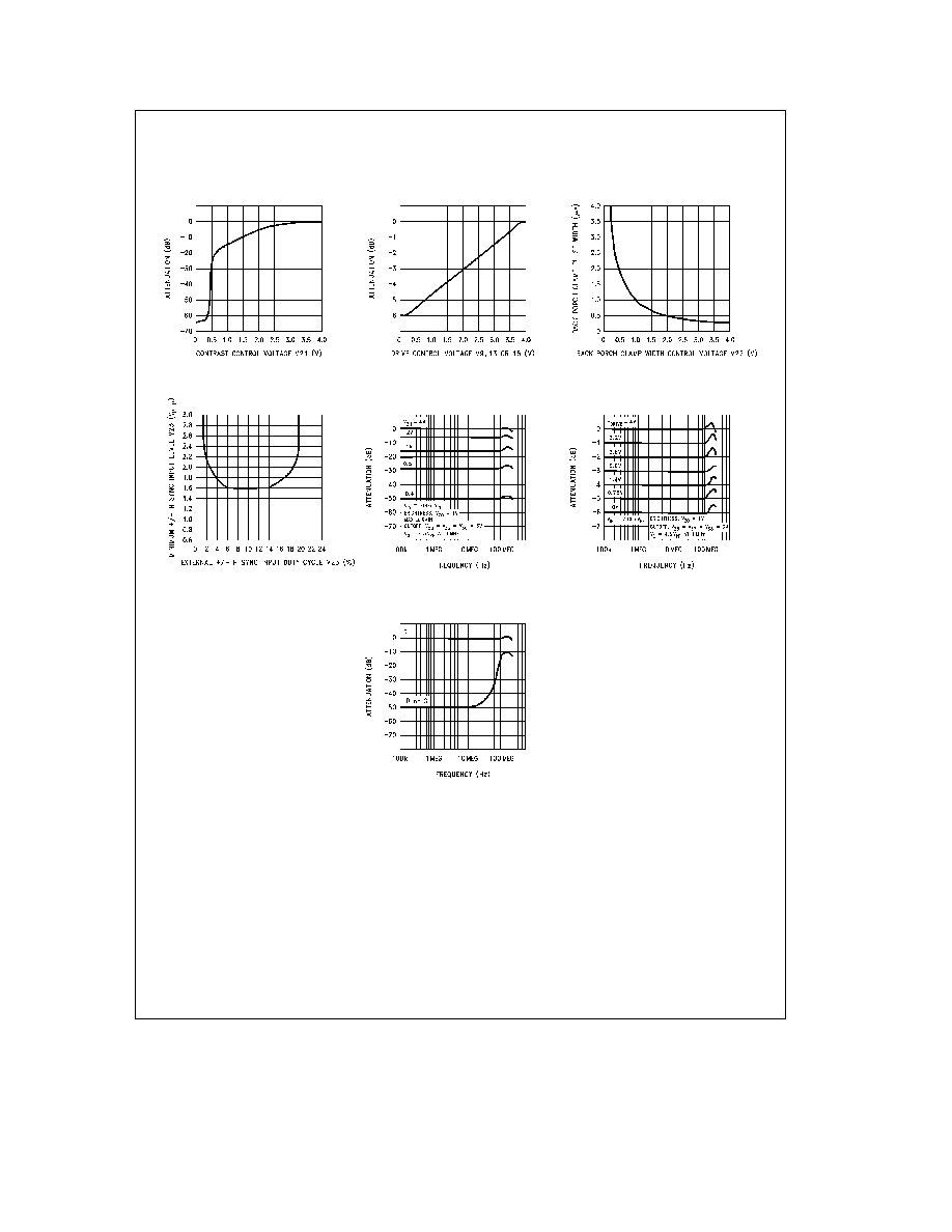
Typical Performance Characteristics
V
CC
e
12V T
A
e
25 C unless otherwise specified
Control Voltage (
f e
12 kHz)
Attenuation vs Contrast
Control Voltage (
f e
12 kHz)
Attenuation vs Drive
Width vs Pin 22 Voltage
Back Porch Clamp Pulse
vs Input Duty Cycle (%)
Sync Input Level (V
PP
)
Minimum External
g
H
Contrast vs Frequency
Drive Control vs Frequency
Crosstalk vs Frequency
TL H 11238 ≠ 2
5