
TL H 11881
LM1205LM1207
130
MHz85
MHz
RGB
Video
Amplifier
System
with
Blanking
January 1996
LM1205 LM1207
130 MHz 85 MHz RGB Video Amplifier System with
Blanking
General Description
The LM1205 LM1207 is a very high frequency video amplifi-
er system intended for use in high resolution RGB monitor
applications In addition to the three matched video amplifi-
ers the LM1205 LM1207 contains three gated single end-
ed input black level clamp comparators for brightness con-
trol three matched DC controlled attenuators for contrast
control and three DC controlled sub-contrast attenuators
providing gain trim capability for white balance All DC con-
trol inputs offer high input impedance and an operation
range from 0V to 4V for easy interface to bus controlled
alignment systems The LM1205 LM1207 also contains a
blanking circuit which clamps the video output voltage dur-
ing blanking to within 0 1V above ground This feature pro-
vides blanking capability at the cathodes of the CRT A spot
killer is provided for CRT phosphor protection during power-
down
Features
Y
Three wideband video amplifiers 130 MHz (LM1205)
b
3 dB (4 V
PP
output)
Y
Matched (
g
0 1 dB or 1 2%) attenuators for contrast
control
Y
Three externally gated single ended input comparators
for cutoff and brightness control
Y
0V to 4V high input impedance DC contrast control
(
l
40 dB range)
Y
0V to 4V high input impedance DC drive control for
each video amplifier (
b
6 dB to 0 dB range)
Y
Spot killer blanks output when V
CC
k
10 6V
Y
Capable of 7 V
PP
output swing (slight reduction in
bandwidth)
Y
Output stage blanking
Y
Output stage directly drives most hybrid or discrete
CRT drivers
Applications
Y
High resolution RGB CRT monitors
Y
Video AGC amplifiers
Y
Wideband amplifiers with gain and DC offset controls
Y
Interface amplifiers for LCD or CCD systems
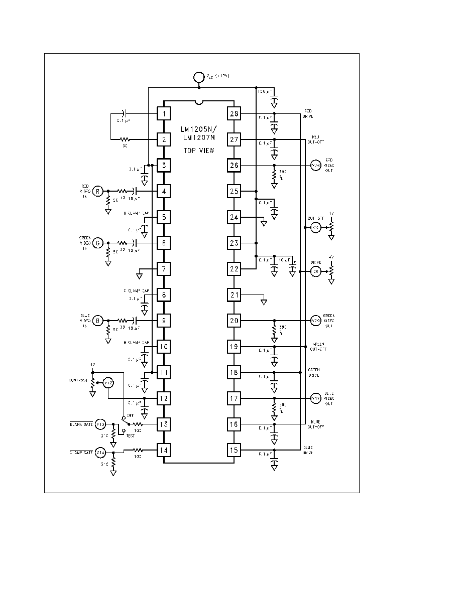
Block and Connection Diagram
TL H 11881 � 1
FIGURE 1
Order Number LM1205N or LM1207N
See NS Package Number N28B
C1996 National Semiconductor Corporation
RRD-B30M66 Printed in U S A
Absolute Maximum Ratings
(Note 1)
If Military Aerospace specified devices are required
please contact the National Semiconductor Sales
Office Distributors for availability and specifications
Supply Voltage (V
CC
)
Pins 3 11 22 23 25 (Note 3)
15V
Peak Video Output Source Current
(Any One Amp) Pins 17 20 or 26
28 mA
Voltage at Any Input Pin (V
IN
)
V
CC
t
V
IN
t
GND
Power Dissipation (P
D
)
(Above 25 C Derate Based on i
JA
and T
J
)
2 5W
Thermal Resistance (i
JA
)
50 C W
Junction Temperature (T
J
)
150 C
ESD Susceptibility (Note 4)
2 kV
Pins 12 13 and 14
1 9 kV
Storage Temperature
b
65 C to 150 C
Lead Temperature (Soldering 10 sec )
265 C
Operating Ratings
(Note 2)
Temperature Range
b
20 C to 80 C
Supply Voltage (V
CC
)
10 8V
s
V
CC
s
13 2V
DC Electrical Characteristics
See DC Test Circuit
(Figure 2 ) T
A
e
25 C V
CC1
e
V
CC2
e
12V V
12
e
4V
V
14
e
0V V
cut-off
e
1 0V V
13
e
4V V
drive
e
4V unless otherwise stated
Symbol
Parameter
Conditions
Typical
Limit
Units
(Note 5)
(Note 6)
I
S
Supply Current
V
CC1
a
V
CC2
R
L
e
%
(Note 7)
90
105
mA (max)
V
4 6 9
Video Amplifier Input Bias Voltage
2 8
V
R
IN
Video Input Resistance
Any One Amplifier
20
kX
V
14l
Clamp Gate Low Input Voltage
Clamp Comparators On
1 2
0 8
V (max)
V
14h
Clamp Gate High Input Voltage
Clamp Comparators Off
1 6
2 0
V (min)
I
14l
Clamp Gate Low Input Current
V
14
e
0V
b
1
b
5
m
A (max)
I
14h
Clamp Gate High Input Current
V
14
e
12V
0 01
1 0
m
A (max)
I
clamp
Clamp Cap Charge Current
Clamp Comparators On
g
750
g
500
m
A (min)
I
bias
Clamp Cap Bias Discharge Current
Clamp Comparators Off
500
nA
V
13l
Blank Gate Low Input Voltage
Blank Gate On
1 2
0 8
V (max)
V
13h
Blank Gate High Input Voltage
Blank Gate Off
1 6
2 0
V (min)
I
13l
Blank Gate Low Input Current
V
13
e
0V
b
8 5
b
11 0
m
A (max)
I
13h
Blank Gate High Input Current
V
13
e
12V
0 01
1 0
m
A (max)
V
OL
Video Output Low Voltage
V
cut-off
e
0V
0 15
0 5
V (max)
V
OH
Video Output High Voltage
V
cut-off
e
9V
7 5
7
V (min)
V
O(1V)
Video Black Level Output Voltage
V
cut-off
e
1V
1 0
V (Note 8)
D
V
O(1V)
Video D Black Level Output Voltage
Between Any Two Amplifiers
g
100
mV (max)
V
cut-off
e
1V
V
OL
(blanked)
Video Output Blanked Voltage
V
13
e
0V
35
70
mV (max)
I
12 15 18 or 28
Contrast Drive Control Input Current
V
contrast
e
V
drive
e
0V to 4V
b
250
nA
I
16 19 and 27
Cut-Off Control Input Current (All Inputs)
V
cut-off
e
0V to 4V
b
500
nA
V
spot
Spot Killer Voltage
V
CC
Adjusted to Activate
10 4
10 8
V (max)
http
www national com
2
AC Electrical Characteristics
See AC Test Circuit
(Figure 3) T
A
e
25 C V
CC1
e
V
CC2
e
12V Manually
adjust Video Output pins 17 20 and 26 to 4V DC for the AC test unless otherwise stated (Note 14)
Symbol
Parameter
Conditions
Typical
Limit
Units
(Note 5)
(Note 6)
A
V max
Video Amplifier Gain
V12
e
4V V
IN
e
635 mV
PP
7 0
6 0
V V (min)
V
drive
e
4V
16 9
15 6
dB (min)
D
A
V 2V
Attenuation
2V
Ref A
V
max V12
e
2V
b
6
dB
D
A
V 0 25V
Attenuation
0 25V
Ref A
V
max V12
e
0 25V
b
40
dB
D
Drive
Drive Control Range
V
drive
e
0V to 4V V12
e
4V
6
dB
A
V match
Absolute Gain Match
A
V
max
V12
e
4V V
drive
e
4V (Note 9)
g
0 3
dB
A
V track1
Gain Change Between Amplifiers
V12
e
4V to 2V (Notes 9 10)
g
0 1
dB
THD
Video Amplifier Distortion
V
O
e
1 V
PP
f
e
10 kHz
1
%
f (
b
3 dB)
Video Amplifier Bandwidth
V12
e
4V V
drive
e
4V
LM1205
130
MHz
(Notes 11 12)
V
O
e
4 V
PP
LM1207
85
t
r
(Video)
Video Output Rise Time (Note 11)
V
O
e
4 V
PP
LM1205
2 6
ns
LM1207
4 3
t
f
(Video)
Video Output Fall Time (Note 11)
V
O
e
4 V
PP
LM1205
3 6
ns
LM1207
4 3
V
sep
10 kHz
Video Amplifier 10 kHz Isolation
V12
e
4V (Note 13)
b
70
dB
V
sep
10 MHz
Video Amplifier 10 MHz Isolation
V12
e
4V (Notes 11 13)
b
50
dB
t
r
(Blank)
Blank Output Rise Time (Note 11)
Blank Output
e
1 V
PP
7
ns
t
f
(Blank)
Blank Output Fall Time (Note 11)
Blank Output
e
1 V
PP
7
ns
t
pw
(Clamp)
Min Back Porch Clamp Pulse Width
200
ns
Note 1
Absolute Maximum Ratings indicate limits beyond which damage to the device may occur
Note 2
Operating Ratings indicate conditions for which the device is functional but do not guarantee specific performance limits For guaranteed specifications
and test conditions see the Electrical Characteristics The guaranteed specifications apply only for the test conditions listed Some performance characteristics
may degrade when the device is not operated under the listed test conditions
Note 3
V
CC
supply pins 3 11 22 23 25 must be externally wired together to prevent internal damage during V
CC
power on off cycles
Note 4
Human body model 100 pF discharged through a 1 5 kX resistor
Note 5
Typical specifications are specified at
a
25 C and represent the most likely parametric norm
Note 6
Tested limits are guaranteed to National's AOQL (Average Outgoing Quality Level)
Note 7
The supply current specified is the quiescent current for V
CC1
and V
CC2
with R
L
e
%
see
Figure 2's test circuit The supply current for V
CC2
(pin 23) also
depends on the output load With video output at 1V DC the additional current through V
CC2
is 8 mA for
Figure 2's test circuit
Note 8
Output voltage is dependent on load resistor Test circuit uses R
L
e
390X
Note 9
Measure gain difference between any two amplifiers V
IN
e
635 mV
PP
Note 10 D
A
V
track is a measure of the ability of any two amplifiers to track each other and quantifies the matching of the three attenuators It is the difference in
gain change between any two amplifiers with the contrast voltage (V12) at either 4V or 2V measured relative to an A
V
max condition V12
e
4V For example at A
V
max the three amplifiers' gains might be 17 1 dB 16 9 dB and 16 8 dB and change to 11 2 dB 10 9 dB and 10 7 dB respectively for V12
e
2V This yields the
measured typical
g
0 1 dB channel tracking
Note 11
When measuring video amplifier bandwidth or pulse rise and fall times a double sided full ground plane printed circuit board without socket is
recommended Video amplifier 10 MHz isolation test also requires this printed circuit board The reason for a double sided full ground plane PCB is that large
measurement variations occur in single sided PCBs
Note 12
Adjust input frequency from 10 MHz (A
V
max reference level) to the
b
3 dB corner frequency (f
b
3 dB
)
Note 13
Measure output levels of the other two undriven amplifiers relative to the driven amplifier to determine channel separation Terminate the undriven
amplifier inputs to simulate generator loading Repeat test at f
IN
e
10 MHz for V
sep 10 MHz
Note 14
During the AC tests the 4V DC level is the center voltage of the AC output signal For example if the output is 4 V
PP
the signal will swing between 2V DC
and 6V DC
http
www national com
3
Typical Performance Characteristics
V
CC
e
12V T
A
e
25 C unless otherwise specified
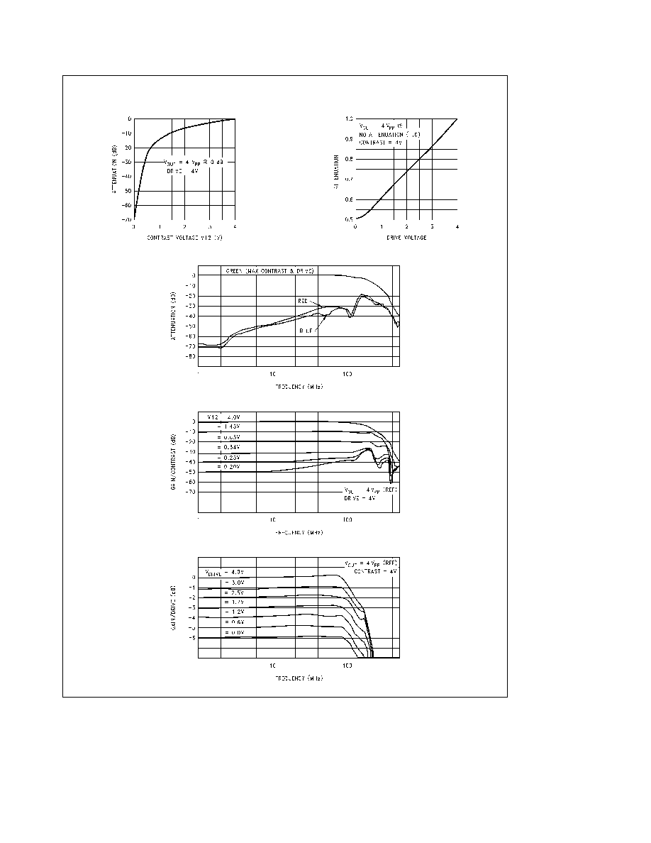
Attenuation vs Contrast Voltage
TL H 11881 � 2
Attenuation vs Drive Voltage
TL H 11881 � 3
LM1205 Crosstalk vs Frequency
TL H 11881 � 4
LM1205 Contrast vs Frequency
TL H 11881 � 5
LM1205 Drive vs Frequency
TL H 11881 � 6
http
www national com
4
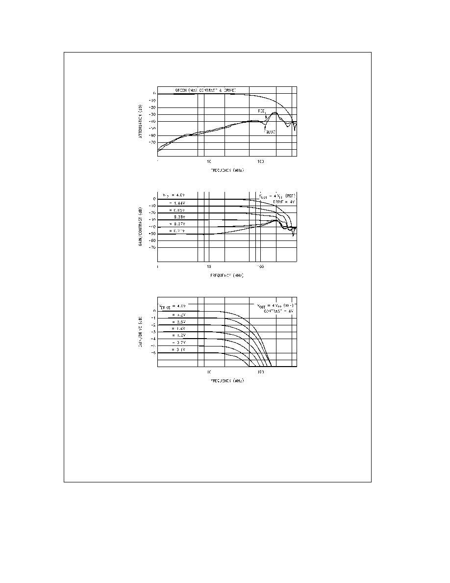
Typical Performance Characteristics
V
CC
e
12V T
A
e
25 C unless otherwise specified (Continued)
LM1207 Crosstalk vs Frequency
TL H 11881 � 7
LM1207 Contrast vs Frequency
TL H 11881 � 8
LM1207 Drive vs Frequency
TL H 11881 � 9
http
www national com
5
Applications Information
TL H 11881 � 10
FIGURE 2 LM1205N LM1207N DC Test Circuit
http
www national com
6

Applications Information
(Continued)
TL H 11881 � 11
FIGURE 3 LM1205N LM1207N AC Test Circuit
http
www national com
7

Applications Information
(Continued)
TL H 11881 � 12
FIGURE 4 LM1205N LM1207N PCB Test Circuit
http
www national com
8
Applications Information
(Continued)
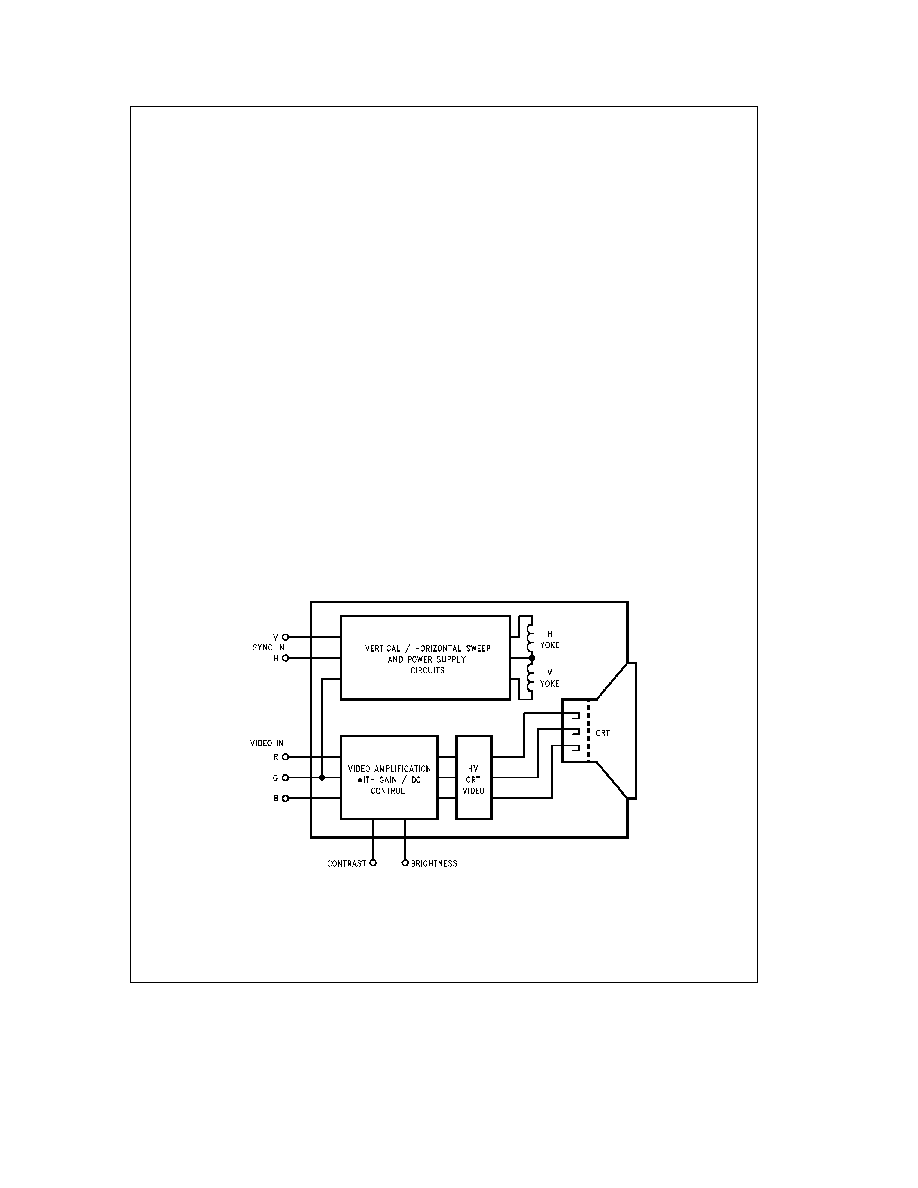
Figure 5 shows the block diagram of a typical analog RGB
color monitor The RGB monitor is used with CAD CAM
work stations PC's arcade games and in a wide range of
other applications that benefit from the use of color display
terminals The RGB color monitor characteristics may differ
in such ways as sweep rates screen size CRT color trio
spacing (dot pitch) or in video amplifier bandwidths but will
still be generally configured as shown in
Figure 5 Separate
horizontal and vertical sync signals may be required or they
may be contained in the green video input signal The video
input signals are usually supplied by coax cable which is
terminated into 75X at the monitor input and internally AC
coupled to the video amplifiers These input signals are ap-
proximately 1V peak to peak in amplitude and at the input of
the high voltage video section approximately 5V peak to
peak At the cathode of the CRT the video signals can be as
high as 60V peak to peak One important requirement of the
three video amplifiers is that they match and track each
other over the contrast and brightness control range The
Figure 5 block labeled ``VIDEO AMPLIFICATION WITH
GAIN AND DC CONTROL'' describes the function of the
LM1205 LM1207 which contains the three matched video
amplifiers contrast control and brightness control The
LM1205 LM1207 also provides the capability to blank at the
cathode of the CRT
Functional Description
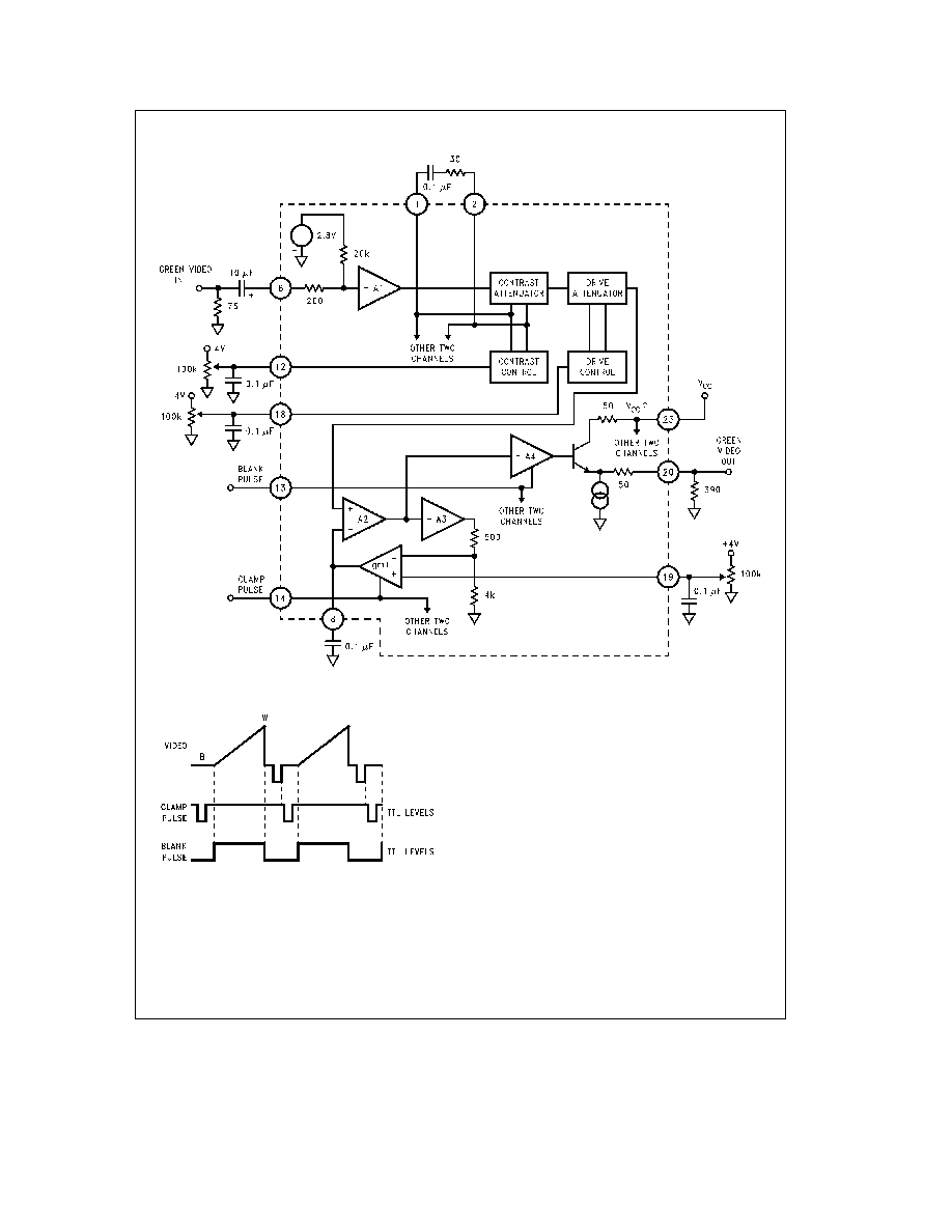
Figure 6 is a detailed block diagram of the green channel of
the LM1205 LM1207 along with the recommended external
components The IC pin numbers are circled and all external
components are shown outside the dashed line The other
two video channels are identical to the green channel only
the numbers to the pins unique to each channel are differ-
ent The input video is normally terminated into 75X The
termination resistor depends on the impedance of the coax
cable being used 75X being the most common impedance
used in video applications The video signal is AC coupled
through a 10 mF capacitor to the input pin 6 There is no
standard for the DC level of a video signal therefore the
signal must be AC coupled to the LM1205 LM1207 Internal
to the LM1205 LM1207 is a 2 8V reference giving the input
video an offset voltage of 2 8V This voltage was selected to
give the input video enough DC offset to guarantee that the
lowest voltage of the video signal at pin 6 is far enough
above ground to keep the LM1205 LM1207 in the active
region The 200X resistor at the input is for ESD protection
and for current limiting during any voltage surge that may
occur at the input driving pin 6 above V
CC
The input video
signal is buffered by
b
A1 In this circuit description an in-
verting amplifier is shown with a ``
b
'' (minus sign) in front of
the amplifier designation The output of
b
A1 goes to the
contrast and drive attenuator sections
The contrast and drive control sections are virtually identi-
cal Both sections take a 0V to 4V input voltage 4V giving
the maximum gain for either the contrast or the drive This is
a high impedance input allowing for an easy interface to 5V
DACs One may also use 100k potentiometers with no deg-
radation in performance The contrast control section is
common to all three channels It converts the input voltage
at pin 12 to a couple of internal DC voltages that control the
gain of the contrast attenuator Referring to the Attenuation
vs Contrast Voltage under typical performance characteris-
tics note that a 4V control voltage results in no attenuation
of the video signal A 0 25V control voltage results in an
attenuation of 40 dB Again note that these internal control
voltages are common to all three channels To minimize
crosstalk these voltages go to pins 1 and 2 Minimizing
crosstalk is done by adding the RC network shown in the
block diagram
(Figure 6)
TL H 11881 � 13
FIGURE 5 Typical RGB Color Monitor Block Diagram
http
www national com
9

Functional Description
(Continued)
The 0V to 4V drive control signal comes in on pin 18 Each
channel has its own drive section therefore the crosstalk
compensation needed for the contrast control voltages is
not required for the drive control thus no external pins for
the drive control The drive attenuator gives an attenuation
range from 0 dB to
b
6 dB A small gain adjustment range
for the drive attenuator is desirable and intentionally de-
signed because the drive is used only to balance the overall
gain of each color channel giving the correct color tempera-
ture on the CRT
The output of the drive attenuator stage goes to A2 the
amplifier in the DC restoration section The video signal
goes to the non-inverting input of A2 The inverting side of
A2 goes to the output of gm1 the clamp comparator and
the clamp capacitor at pin 8
During the back porch period of the video signal a negative
going clamp pulse from pin 14 is applied to the clamp com-
parator turning on the comparator This period is where the
black level of the video signal at the output of the LM1205
LM1207 is compared to the desired black level which is set
at pin 19
Figure 7 shows the timing of the clamp pulse
relative to the video signal The clamp capacitor is charged
or discharged by gm1 generating the correction voltage
needed at the inverting input of A2 to set the video output to
the correct DC level Removing the clamp pulse turns off
gm1 with the correction voltage being maintained by the
clamp capacitor during active video Both the clamp pulse
and the blank pulse at pin 13 are TTL voltage levels
There are actually two output sections
b
A3 and
b
A4 Both
sections have been designed to be identical except
b
A4
has more current drive capability The output transistor
shown is part of
b
A4 but has been shown separately so
the user knows the configuration of the output stage
b
A3
does not go to the outside world it is used for feeding back
the video signal for DC restoration Its output goes directly
to the inverting input of the clamp comparator via the volt-
age divider formed by the 500X and 4k resistors
b
A4 will
be close to the same output as
b
A3 and will temperature
track due to the similar design of the two output stages
However the current at the output of
b
A4 will be ten times
the current at the output of
b
A3 To balance both outputs a
load resistance of 390X needs to be connected from pin 20
the green video output pin to ground Another input to
b
A4
is the blank pulse When a negative going blank pulse is
applied to pin 13 the output of the LM1205 LM1207 is driv-
en to less than 0 1V above ground Using the timing shown
in
Figure 7 for the blank pulse the output of the LM1205
LM1207 will be less than 0 1V during the inactive portion of
the video signal This is a ``blacker than black'' condition
blanking the CRT at the cathodes By using the blank func-
tion of the LM1205 LM1207 no grid blanking is necessary
Note that the DC restoration is done by feeding back the
video signal from
b
A3 but blanking is done at
b
A4 By
using the two output stages blanking can be done at the
CRT cathodes and at the same time activate the DC resto-
ration loop
V
CC1
goes to pins 3 11 and 25 (see
Figure 1 ) These three
pins are all internally connected For proper operation of the
LM1205 LM1207 it is necessary to connect all the V
CC1
pins to the input power to the PCB and bypass each pin with
a 0 1 mF capacitor V
CC2
is the input power at pins 22 and
23 for the three output stages This is a separate power
input from V
CC1
there are no internal connections between
the two different power inputs There must be a connection
on the PCB between V
CC1
and V
CC2
Pins 22 and 23 must
be bypassed by a parallel connection of a 10 mF and 0 1 mF
capacitors
The ground connections for the LM1205
LM1207 are at pins 7 21 and 24 All three ground pins are
internally connected and these pins must also be connect-
ed externally to a good ground plane for proper operation of
the LM1205 LM1207
http
www national com
10
Functional Description
(Continued)
TL H 11881 � 14
FIGURE 6 Block Diagram of LM1205 LM1207 Video Amplifier
TL H 11881 � 15
FIGURE 7 Timing Diagram
Circuit Description
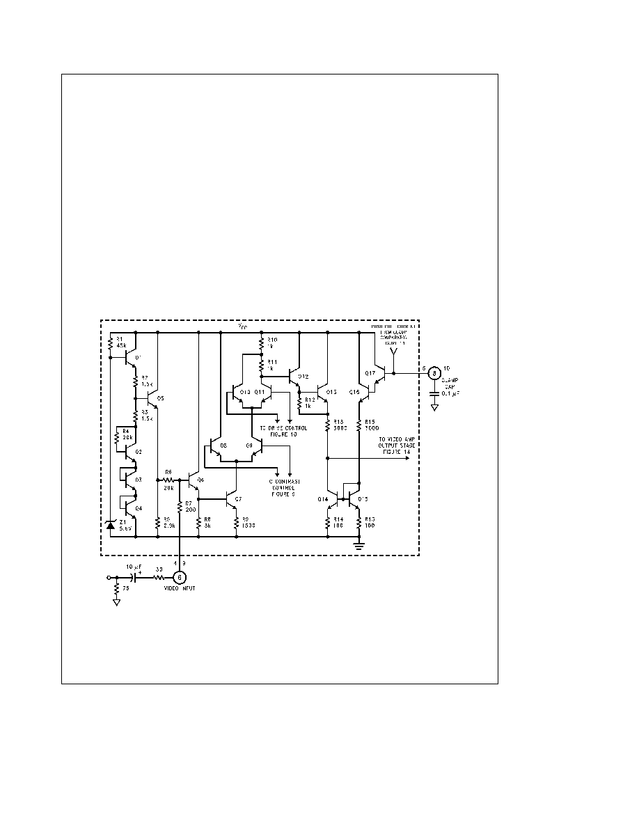
VIDEO AMPLIFIER INPUT STAGE
Figure 8 is a simplified schematic of one of the three video
amplifiers input stage along with the recommended external
components The IC pin numbers are circled and all external
components are shown outside the dashed line The video
input is applied to pin 6 via a 10 mF coupling capacitor and a
30X resistor The resistor is added to limit the current
through the input pin should an applied voltage surge rise
above V
CC
or drop below ground The performance of the
LM1205 LM1207 is not degraded by the 30X resistor How-
ever if EMI is a concern this resistor can be increased to
well over 100X where the rise and fall times will start to
become longer DC bias to the input pin is provided by Q5
and its associated input circuitry Z1 is a 5 6V zener that
generates the input bias voltage Q1 is a buffer to the zener
reference voltage with 5 0V generated at its emitter Q3 and
Q4 are connected as diodes Q2 is close to being a diode in
this circuit This configuration will give about 2 0V at the
collector of Q2 R2 and R3 are a voltage divider setting the
base of Q5 to about 3 5V This sets the emitter of Q5 to
about 2 8V the bias voltage of the video input This bias
voltage is necessary to assure that the entire video signal
stays within the active operating region of the LM1205
LM1207 The bias voltage goes through R6 a 20k resistor
to the video input at pin 6 R4 and R6 are of the same value
http
www national com
11
Circuit Description
(Continued)
and R4 is used to compensate for beta variations of the
transistors Note that the bias voltage passes through three
diode drops (Q5 Q6 and Q7) before setting the voltage
across R9 Q2 Q3 and Q4 also provide three diode drops
to the bias voltage at the base of Q5 temperature compen-
sating for the diode drops of Q5 Q6 and Q7 This insures
that the bias voltage across R9 remains very constant over
temperature providing an accurate bias current for the dif-
ferential transistor pair Q8 and Q9 thus assuring proper op-
eration of the contrast control
Q6 serves as a buffer to the input video signal Its emitter
drives the base of Q7 Thus the video signal modulates the
current flowing through R9 which in turn modulates the cur-
rents through the differential pair formed by Q8 and Q9 The
current flow through Q8 and Q9 is controlled by a DC volt-
age from the Contrast Control circuit This DC voltage is
common to all three channels Increasing the voltage to the
base of Q9 with respect to the base of Q8 increases the
current flow through Q9 A higher current flow through Q9
increases the video gain (contrast) of the LM1205 LM1207
Q10 and Q11 also form a differential pair at the collector of
Q9 The operation of this differential pair is similar to Q8 and
Q9 The DC control voltage is from the Drive Control cir-
cuits Each channel has its own drive control circuit In-
creasing the voltage to the base of Q11 increases the video
gain (drive) of the LM1205 LM1207 R10 and R11 are of
the same value but R10 is common to both Q10 and Q11 If
all the current is flowing through Q10 the video amplitude
would only be half of the maximum gain (all current flowing
through Q11) This gives the drive control a total gain ad-
justment range of 6 dB Since the drive control is only used
to balance the color of each channel a small adjustment
range is desirable Q12 through Q17 are part of the final
section shown in
Figure 8 DC restoration is done at this
stage The clamp comparator
(Figure 11) drives the clamp
cap at pin 8 to a voltage that sets the correct black level of
the video signal This cap is also connected to the base of
Q17 Q17 and Q16 are one half of the darlington differential
pair The clamp cap voltage establishes the current flow
through R16 Q15 and R15 With the bases of Q14 and
Q15 held to the same voltage the current through Q15 is
mirrored into Q14 and the other half of the differential pair
Q12 and Q13 By this current mirror the voltage at the col-
lector of Q14 is set to the correct DC value for the video
signal by controlling the voltage drop across R13 complet-
ing the DC restoration
TL H 11881 � 16
FIGURE 8 Simplified Schematic of LM1205 LM1207 Video Amplifier Input Stage
http
www national com
12

Circuit Description
(Continued)
CONTRAST CONTROL
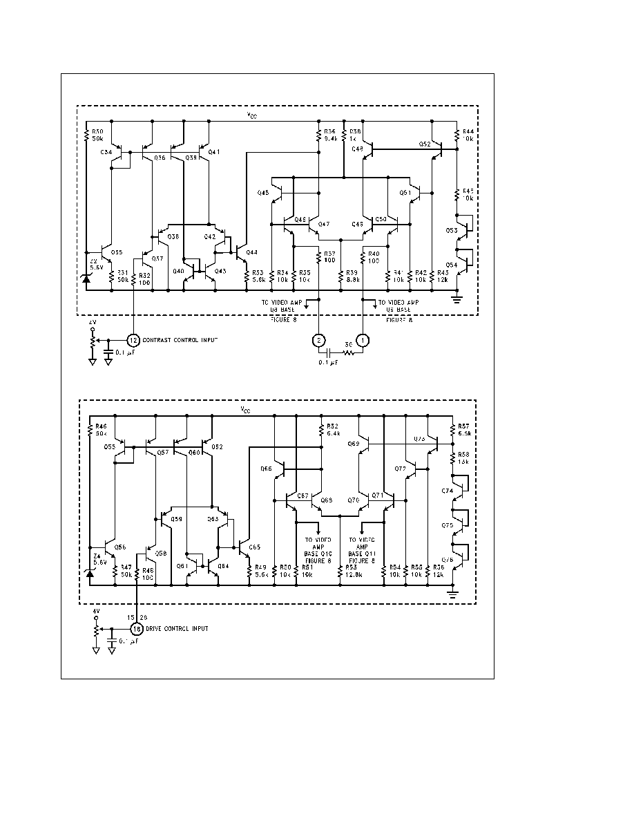
Figure 9 is a simplified schematic of the Contrast Control
circuit The output of this circuit is common to all three chan-
nels A reference voltage is generated by Z2 Q34 Q35
R30 and R31 Q36 Q39 and Q41 are all current sources
that are controlled by the reference voltage The contrast
signal has a 0V to 4V range with its input at pin 12 R32 is
used for current limiting any voltage surge that may occur at
pin 12 Note that the input stage (Q37 Q38 and Q42) are
all PNP transistors This configuration is necessary for oper-
ation down to near ground At Q44 the input voltage is con-
verted to a current by R33 The input stage will apply the
same voltage across R33 as is applied at the input and with
no temperature variations from the transistors Q37 is con-
nected to a current source (Q36) to keep a constant current
flow through Q37 and a predictable diode voltage for the
base-emitter of Q37 Q40 is connected as a diode and is
biased by the current source Q39 The current through Q40
is mirrored into Q43 giving a current bias for Q42 Again this
is done to give a predictable diode voltage for Q42 Q41 is a
current source for both Q38 and Q42 With the current
through Q42 already established the rest of the current
from Q41 flows through Q38 As one can see the input volt-
age is accurately reflected across R33 with no temperature
coefficients from the input stage of the contrast control cir-
cuit
Pin 1 of the contrast control output is held at a constant
voltage two diode drops below
V
CC
To generate this ref-
erence the base of Q51 is held at exactly
V
CC
R44 and
R45 form a voltage divider With both Q53 and Q54 con-
nected as diodes the voltage at the junction of R44 and R45
is
V
CC
plus one diode drop Q52 is a buffer to this refer-
ence voltage generating exactly
V
CC
at its emitter Q51 is
used to drive the bases of Q49 and Q50 to one diode drop
below the reference voltage Q50 is used to further buffer
the reference voltage to the base of Q9 (see
Figure 8 ) and
the corresponding transistors in the other channels Q48 is
used to bias the collector of Q49 to
V
CC
the same volt-
age as the collector of Q47 when the differential pair is bal-
anced This keeps the characteristics of Q47 and Q49 well
matched Going back to Q44 and R33 these parts set up a
current source that varies the current through R36 With a
2V contrast voltage the differential pair is balanced mean-
ing that the voltage drop across R36 is
V
CC
Q45 buffers
the voltage at R36 driving the bases of Q46 and Q47 Q46
further buffers the voltage driving the base of Q8 (see
Fig-
ure 8 ) and the corresponding transistors in the other two
channels In the balanced condition the voltage at pin 2 will
also be two diode drops below
V
CC
giving a well bal-
anced drive to the differential pair consisting of Q8 and Q9
in the video amplifier input stage With the contrast voltage
set to 0V the voltage at pin 2 will increase by about 400 mV
to 500 mV A 4V contrast voltage decreases the voltage at
pin 2 by about 400 mV to 500 mV from the balanced condi-
tion Reviewing
Figure 8 note that decreasing the voltage at
pin 2 will decrease the current flow through Q8 Thus the
current flow through Q9 increases increasing the gain of
the LM1205 LM1207 So increasing the contrast control
voltage at pin 12 increases the gain of the LM1205
LM1207 The contrast control voltage from Q46 and Q50 is
common to all three channels To minimize crosstalk it is
necessary to add a decoupling capacitor of 0 1 mF across
R37 and R40 Since this can only be done externally these
two nodes are brought out to pins 1 and 2 The 30X resistor
is added in series with the capacitor for improving stability
To prevent a destructive current surge due to shorting either
pins 1 or 2 to ground R38 was added for current limiting
DRIVE CONTROL
Figure 10 is a simplified schematic of the Drive Control cir-
cuit Each channel has its own drive control circuit This
circuit is almost identical to
Figure 9 the contrast control
circuit It will be easier to cover the differences between the
two circuits instead of going through virtually the same cir-
cuit description Note that the input stage is exactly the
same The generation of the reference voltage at the right
hand side of
Figure 10 is slightly different than the circuit in
Figure 9 ln the drive control circuit the reference voltage at
the base of Q72 is to be
V
CC
In the contrast control
circuit the reference voltage at the base of Q51 was to be
V
CC
To generate the
V
CC
R57 and R58 form a 2 to 1
voltage divider With the two to one ratio it is now necessary
to have three transistors connected as diodes which are
Q74 Q75 and Q76 Q73 is the buffer for this voltage divider
and its emitter is exactly
V
CC
with temperature compen-
sation R52 and R53 also differ from their corresponding
resistors in
Figure 9 R36 and R39 The value difference is
so the base of Q66 is also at
V
CC
when the input drive
voltage is at 2V R38 in
Figure 9 was needed for current
limiting at the output pins Since each channel has its own
drive control circuit no filtering is required eliminating the
need for external pins With no external pins no current limit-
ing is necessary thus the 1k resistor is not used in the drive
control circuit
http
www national com
13
Circuit Description
(Continued)
TL H 11881 � 17
FIGURE 9 Simplified Schematic of LM1205 LM1207 Contrast Control
TL H 11881 � 18
FIGURE 10 Simplified Schematic of LM1205 LM1207 Drive Control
http
www national com
14

Circuit Description
(Continued)
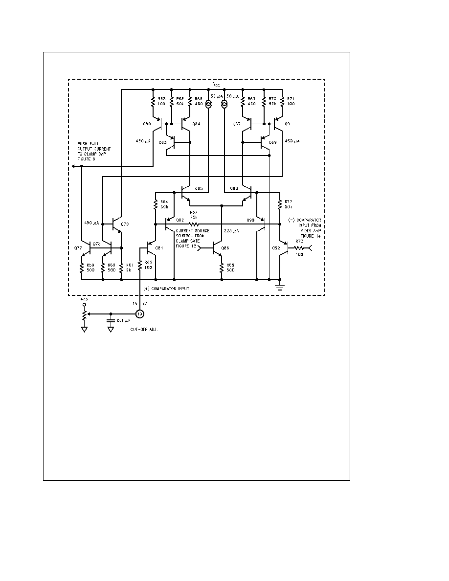
CLAMP COMPARATOR CIRCUIT
Figure 11 is a simplified schematic of the clamp comparator
circuit Q85 and its input transistors Q81 and Q82 are one
half of the differential pair The base of Q81 is connected to
pin 19 via R62 This is the positive input to the comparator
Q88 and its input transistors Q90 and Q91 are the other
half of the differential pair The base of Q92 is connected to
the junction of R19 and R20 in
Figure 14 via R73 This is the
negative input to the comparator R73 is included only to
match the input characteristics of the positive input which
requires the 100X resistor The negative comparator input is
the feedback from the output stage as briefly described in
the block diagram and covered in more detail in the output
stage circuit description Q86 is the current source for the
differential pair It is turned on and off by the output of the
clamp gate circuit
(Figure 12) Q102 of the clamp gate cir-
cuit has a current flow of about 225 mA when it is turned on
This current is mirrored into Q86 Assume that the inputs to
the comparator are equal making the differential pair bal-
anced ln this condition Q85 and Q88 each have a current
flow of 113 mA Looking at the Q85 side of the circuit Q84
will also have 113 mA of current flow Q80 is set up as a
current mirror to Q84 but its emitter resistor is one fourth
the emitter resistance of Q84 Thus the current flow for Q80
is four times the current flow thru Q84 or 450 mA Q83 has
been added to help drive the base of Q80 increasing the
accuracy of the current mirror The collector of Q80 directly
charges the capacitor as a current source of 450 mA R65 is
added to discharge the charge stored in the bases of Q80
and Q84 This is necessary to quickly turn off the current
charge of the clamp capacitor as the comparator section is
turned off Q87 Q89 and Q90 work in exactly the same
way However the collector of Q91 drives another current
mirror with the 450 mA This current flows thru Q78 Q77 is a
current mirror with Q78 thus 450 mA also flows thru Q77
Q79 has been added to help drive the base of Q77 again
adding to the accuracy of the current mirror Since Q77 is on
the ground side of the circuit it discharges the clamp
capacitor with 450 mA ln this balanced condition the charge
and discharge current are equal thus the voltage across the
clamp capacitor remains unchanged
Going back to the input stages note that both inputs Q81
and Q92 are driven by a 50 mA current source This keeps
both transistors turned on even when the differential pair
Q85 and Q88 is turned off Q82 and Q90 are added to help
drive the bases of Q85 and Q88 respectively R64 and R72
are added to help discharge the charge stored in the bases
of Q85 and Q88 as these two transistors are turned off
Since the input stage remains active the differential pair is
quickly turned off The comparator can also be more quickly
turned on with the input stages remaining active R67 is
used to assure that the potential difference across the dif-
ferential pair is minimal during turnoff Without R67 there
could be a little extra charge or discharge of the clamp ca-
pacitor during turnoff creating an error in the black level of
the video signal Now assume that the input to pin 19 is
slightly higher than the reference voltage to the negative
input of the comparator The voltage at the base of Q85 is
now higher than the base of Q88 This creates an increased
current flow thru Q85 and an equal decrease of current flow
thru Q88 This current change is multiplied by four in the
increase of current flow thru Q80 Likewise the current flow
thru Q77 and Q91 is decreased by four times the current
change in Q88 ln the extreme case the current flow thru
Q80 can increase to 900 mA and there would be no current
flow thru Q77 Q80 does charge the clamp capacitor thus
the voltage across the capacitor will increase The above is
all reversed when the input to Q92 rises above the input
level of Q81 If the base of Q86 the current source to the
differential pair is forced close to ground then there is no
current flow thru Q86 and the differential pair Q85 and Q88
With the current flow thru the differential pair set the zero
all the current mirrors would also have no current flow Thus
the voltage on the camp capacitor would remain constant
the desired result during active video
http
www national com
15
Circuit Description
(Continued)
TL H 11881 � 19
FIGURE 11 Simplified Schematic of LM1205 LM1207 Clamp Comparator Circuit
CLAMP GATE CIRCUIT
Figure 12 is a simplified schematic of the Clamp Gate cir-
cuit A voltage reference is setup by Z3 and by Q104 and
Q105 connected as diodes generating a 7V base drive to
Q94 Q99 and Q101 Q94 is used to bias the input stage
This stage is designed to accept TTL levels at pin 14 Q95
and Q97 form a differential pair The base of Q97 is set to
2 1V by Q99 driving the voltage divider formed by R77 and
R78 In a balanced condition the base of Q95 is also at
2 1V Q96 is connected as a diode and the current flow thru
it is mirrored into Q98 Also the input to pin 14 would be one
diode drop below 2 1V or around 1 4V R74 is added to the
input for current limiting during any possible voltage surge at
pin 14 With no resistors at the emitters of Q96 and Q98 this
circuit will quickly switch Below 1 4V (1 2V typical) Q95 is
turned on and Q97 is turned off Above 1 4V (1 6V typical)
Q97 is turned on and Q95 is turned off With Q97 turned on
Q100 is also turned on This pulls the current thru R79 to
ground turning off Q102 and Q103 Remember Q102 is a
current mirror to Q86 in the clamp comparator With Q102
turned off the clamp comparator is also turned off When
the input signal goes below 1 2V Q97 and Q100 will be
turned off This allows Q102 to turn on turning on the clamp
http
www national com
16
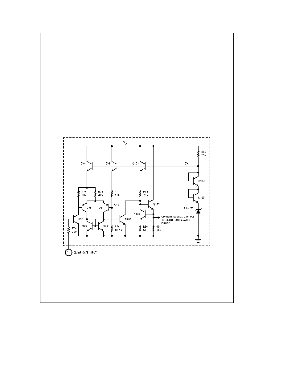
Circuit Description
(Continued)
comparators of the three video channels Q103 is added to
help drive the base of Q86 in the clamp comparator in-
creasing the accuracy of the current mirror Q101 drives
R79 and R80 This sets the current thru Q102 thus setting
the current thru Q86 of the clamp comparator
BLANK GATE CIRCUIT
Figure 13 is a simplified schematic of the Blank Gate circuit
With the exception of the simple output stage and the spot
killer circuit this circuit is almost identical to the clamp gate
circuit The only difference is that the output stage is driven
from the opposite side of the differential pair Thus Q111 is
connected as a diode instead of Q109 With the input at pin
13 at a low level Q108 is turned on also turning on Q29 the
output transistor Q29 is part of the blanking circuit in the
output stage shown in
Figure 14 When Q29 is turned on the
output is clamped to a blanking level that is ``blacker than
black'' allowing blanking to be done on the cathodes of the
CRT
The spot killer circuit is used to force the outputs of the
LM1205 LM1207 into blanking when the V
CC
drops below
10 6V Forcing the outputs to a blacker-than-black level will
drive the cathode driver stage well above the black level
cutting off the beam current in the CRT This prevents the
bright spot from occurring when the monitor is turned off
preserving the phosphor of the CRT The CRT will also have
its beam current cut off during the time the monitor is first
turned on This is not a critical period for the CRT since the
filaments have not warmed up to generate a current flow
The comparator along with R89 R90 and Q115 all form the
spot killer circuit Q115 acts the same as Q106 When Q115
has a high signal at its base it is turned off and the outputs
of the LM1205 LM1207 are in the normal operating mode
A low signal at the base of Q115 turns on this transistor
blanking the outputs of the LM1205 LM1207 Q115 is driv-
en by the output of the comparator The inverting input of
the comparator is connected to an internal 1 2V reference
The non-inverting side is connected to a resistor divider net-
work R89 and R90 When V
CC
is above 10 6V the non-in-
verting input is above the 1 2V reference therefore the out-
put of the comparator is high This high output turns off
Q115 Once the V
CC
drops below 10 6V the comparator's
output goes low turning on Q115 which forces the outputs
into the blanking mode
TL H 11881 � 20
FIGURE 12 Simplified Schematic of LM1205 LM1207 Clamp Gate Circuit
http
www national com
17

Circuit Description
(Continued)
TL H 11881 � 21
FIGURE 13 Simplified Schematic of LM1205 LM1207 Blank Gate Circuit
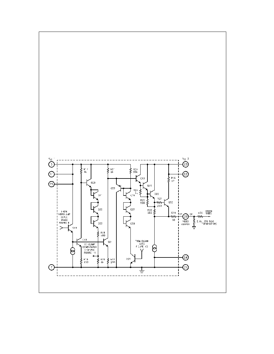
VIDEO AMPLIFIER OUTPUT STAGE WITH BLANK
CIRCUIT
Figure 14 is a simplified schematic of the Video Amplifier
Output Stage including the blanking circuit Q18 serves as a
buffer between the DC restoration stage shown in
Figure 8
and the output stage A current source is used to fix the
current flow thru Q18 keeping it well within its operating
range The emitter of Q18 drives the bases of Q19 and Q24
with the current thru Q24 being twice that of Q19 Q19
along with Q20 thru Q23 duplicate the actual output stage
going to pin 20 Q19 inverts the video signal (note that the
video signal was inverted at Q7 in
Figure 8 ) With two inter-
nal inversions of the video signal in the LM1205 LM1207
the output is non-inverted The collector of Q19 gives a gain
of
b
10 to the video signal and drives the base of Q20 Q21
through Q23 are all connected as diodes with the emitter of
Q23 driving R19 and R20 The junction of R19 and R20 is
connected to the base of Q92 via R73 (shown in
Figure 11 )
this being the feedback to the negative input of the clamp
comparator This stage is independent of the actual output
stage at pin 20 but is where the feedback is done for DC
restoration Therefore it is possible to blank the actual out-
put stage below the black level without affecting the DC
restoration feedback loop Q24 is the equivalent part of Q19
in the actual output stage It also inverts the video signal
with a gain of
b
10 and drives the base of Q30 Q30 thru
Q32 each give a diode drop to the level of the video signal
similar to being connected as diodes Being connected as
emitter-followers these transistors also give current gain to
the signal Q33 comes close to also giving a diode drop to
the signal the voltage drop across R27 being insignificant
R27 has been added to give some isolation between Q33
and the internal circuits of the LM1205 LM1207 adding to
the stability of the device Q33 also has R29 in its emitter for
isolation from capacitive loads and current limiting from any
possible voltage surges R28 is at the collector of Q33 is
also for current limiting from voltage surges and minimizing
crosstalk between the three channels through the V
CC
line
To match the loading of the feedback section the output at
pin 20 should have a load of 390X To minimize power con-
sumption the feedback section uses resistor values 10
times larger than those at pin 20 The current source at the
emitter of Q33 provides for the capability to set the black
level as low as 0 5V
The video signal does go thru a number of diode drops at
the output stage One may be concerned that the tracking
over temperature could be a problem The feedback section
has been designed to temperature track the output stage
The feedback for DC restoration eliminates the temperature
coefficients of the diode junctions The remaining section to
be covered is the blanking section This section comprises
of Q25 thru Q29 Q26 thru Q28 are connected as diodes
Q25 provides current gain to this stage to adequately pull
down the base of Q30 during blanking and also adding an-
other diode potential During blanking the base of Q30 will
be four diode drops above ground plus the saturation volt-
http
www national com
18
Circuit Description
(Continued)
age of Q29 There are also four diode drops from the base
of Q30 to the output pin 20 Therefore during blanking pin
20 will be less than 100 mV above ground enabling the
designer to blank at the cathode of the CRT R23 is added
to quickly turn off Q25 by discharging its base when the
blanking signal is removed
Figure 14 also shows the power and ground pins to the
LM1205 LM1207 All the V
CC1
pins (pins 3 11 25) are all
internally connected together A 0 1 mF bypass capacitor
must be located close to each pin and connected to ground
Further bypassing is done by a 100 mF capacitor This ca-
pacitor needs to be located on the board close to the
LM1205 LM1207 Pins 22 and 23 are the V
CC2
pins A
10 mF and a 0 1 mF bypass capacitors must be located
close to pins 22 and 23 Correct bypassing of pins 22 and
23 is very important If the bypassing is not adequate then
the outputs of the LM1205 LM1207 will have ringing or
even worse they may oscillate The ground side of the by-
pass capacitors at pins 22 and 23 must be returned to a
ground plane with no interruptions from other traces be-
tween these capacitors and the ground pins 21 and 24 of
the LM1205 LM1207
Applications of the LM1205
LM1207
Figure 15 is the schematic of the demonstration board de-
signed at National
Figure 16 is the actual layout of the dem-
onstration board
Note that the schematic shown in
Figure 15 is almost identical to the schematic shown in Fig-
ure 4 The only difference between the two schematics is
that in
Figure 15 each channel has individual adjustments
for both drive and cutoff making this circuit a good design
for monitor applications Each CRT will have a slightly differ-
ent cutoff voltage for each color making it necessary to
provide separate adjustments in order to accurately set the
cutoff for each color The gain of each color of the CRT is
also slightly different if the color temperature of the display
is to be accurately set then each channel of the LM1205
LM1207 must have individual gain adjustments Thus each
channel has its own drive control Once the drive control is
set the gain between the three color channels will closely
track as the contrast is adjusted All the jumpers needed to
design a single sided PC board are shown in the schematic
The resistors and jumpers with no reference designation are
the connections between the PC board and the connectors
mounted on the PC board CN1 thru CN8 are BNC connec-
tors
A 30X resistor is in series with each of the video inputs A
voltage surge may occur at these inputs when either the
inputs are first connected to another system or when the
system is powered up before the monitor is turned on If this
voltage surge exceeds the supply voltage (at ground poten-
tial if the monitor is not powered up) of the LM1205
LM1207 or goes below ground current will flow through the
parasitic devices of the LM1205 LM1207 This current is
limited by the 30X resistors preventing a potential cata-
strophic failure A 100X resistor is added to the Blank Gate
TL H 11881 � 22
FIGURE 14 Simplified Schematic of LM1205 LM1207 Video Amplifier Output Stage with Blank Circuit
http
www national com
19

Applications of the LM1205 LM1207
(Continued)
and Clamp Gate inputs These two resistors also limit the
current during a voltage surge A larger resistor is required
because these inputs are DC coupled allowing the current
to continuously flow into these inputs before the monitor is
turned on 100X resistors are not recommended at the vid-
eo inputs because this resistance value will start to roll off
the frequency response of the LM1205 LM1207
Note that the layout shown in
Figure 16 does have a very
extensive ground plane One must remember that the
LM1205 LM1207 is a 130 MHz 85 MHz part and a single
sided board is difficult to successfully design A ground
plane similar to the layout shown in
Figure 16 must be pro-
vided for good performance of the LM1205 LM1207 when
using either a single sided or double sided board The layout
of this board demonstrates the importance of grounding
The results of this layout are shown in
Figures 17a through
17d In these photographs the LM1205 rise time was 2 25
ns and its fall time was 3 00 ns For the LM1207 the rise
time was 4 10 ns and the fall time 3 85 ns The output was a
4 V
PP
signal and the cutoff voltage was set to 2V The
overshoot will subsequently be filtered out by the loading
effects of the CRT driver stage and the CRT itself When the
LM1205 LM1207 is designed into a video board one must
keep the ground to the CRT driver stage separate from the
ground of the LM1205 LM1207
connecting the two
grounds together only at one point National Semiconductor
also manufactures a line of CRT drivers Please contact Na-
tional for additional information These drivers greatly simpli-
fy the driver design allowing for shorter design cycles Of
course the LM1205 LM1207 can also be designed with a
discrete driver stage
Figure 18 shows a design using a sim-
ple cascode CRT driver The LM1205 LM1207 block would
be the same schematic as shown in
Figure 15
REFERENCES
Zahid Rahim ``Guide to CRT Video Design '' Application
Note 861 National Semiconductor Corp Jan 1993
Ott Henry W
Noise Reduction Techniques in Electronic
Systems John Wiley
Sons New York 1976
TL H 11881 � 23
FIGURE 15 Demonstration Board Schematic
http
www national com
20
Applications of the LM1205 LM1207
(Continued)
TL H 11881 � 24
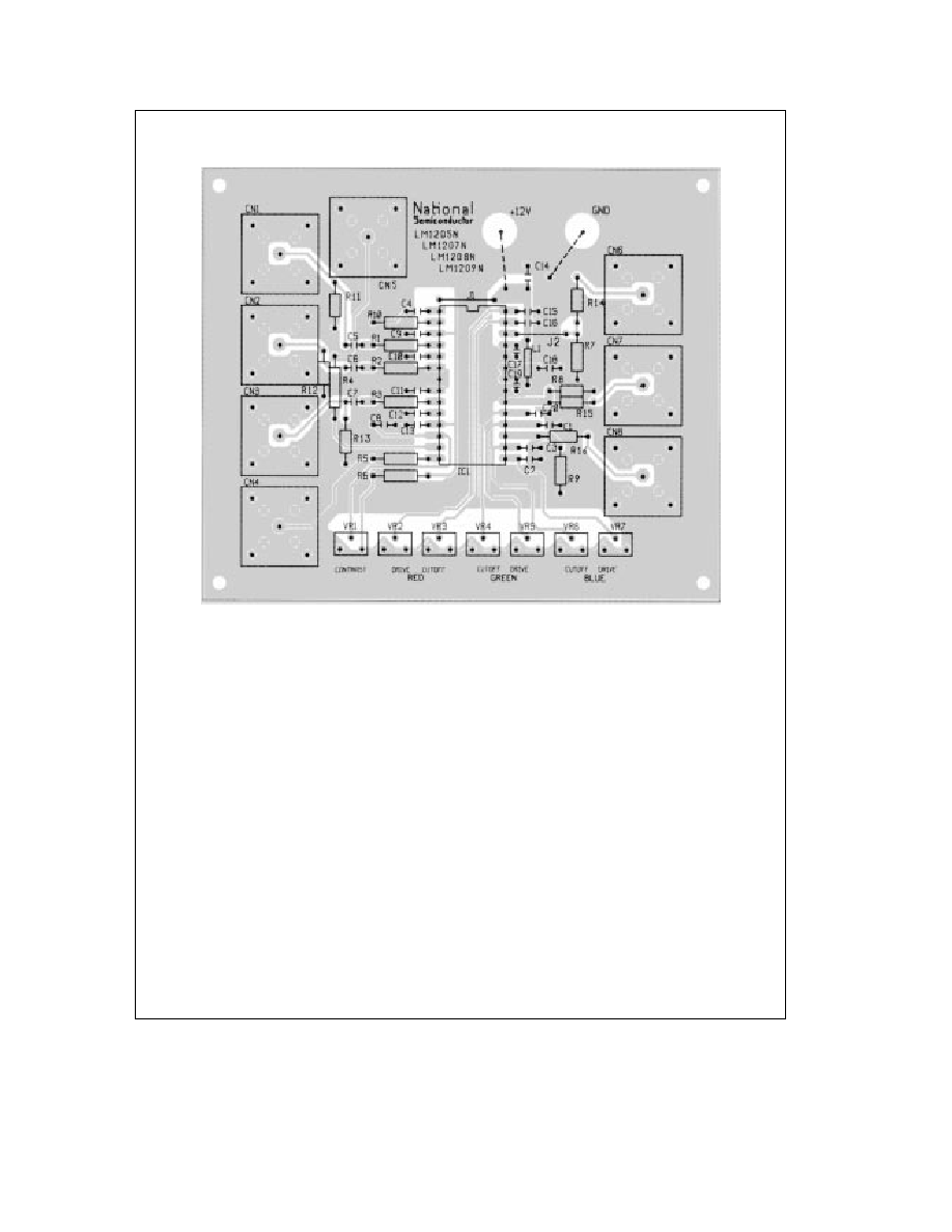
FIGURE 16 Demonstration Board Layout
http
www national com
21

Applications of the LM1205 LM1207
(Continued)
TL H 11881 � 25
FIGURE 17a LM1205 Rise Time
TL H 11881 � 26
FIGURE 17b LM1205 Fall Time
TL H 11881 � 27
FIGURE 17c LM1207 Rise Time
TL H 11881 � 28
FIGURE 17d LM1207 Fall Time
TL H 11881 � 29
FIGURE 18 LM1205 LM1207 Typical Application
http
www national com
22

http
www national com
23

LM1205LM1207
130
MHz85
MHz
RGB
Video
Amplifier
System
with
Blanking
Physical Dimensions
inches (millimeters) unless otherwise noted
Order Number LM1205N or LM1207N
NS Package Number N28B
LIFE SUPPORT POLICY
NATIONAL'S PRODUCTS ARE NOT AUTHORIZED FOR USE AS CRITICAL COMPONENTS IN LIFE SUPPORT
DEVICES OR SYSTEMS WITHOUT THE EXPRESS WRITTEN APPROVAL OF THE PRESIDENT OF NATIONAL
SEMICONDUCTOR CORPORATION As used herein
1 Life support devices or systems are devices or
2 A critical component is any component of a life
systems which (a) are intended for surgical implant
support device or system whose failure to perform can
into the body or (b) support or sustain life and whose
be reasonably expected to cause the failure of the life
failure to perform when properly used in accordance
support device or system or to affect its safety or
with instructions for use provided in the labeling can
effectiveness
be reasonably expected to result in a significant injury
to the user
National Semiconductor
National Semiconductor
National Semiconductor
National Semiconductor
Corporation
Europe
Hong Kong Ltd
Japan Ltd
1111 West Bardin Road
Fax a49 (0) 180-530 85 86
13th Floor Straight Block
Tel 81-043-299-2308
Arlington TX 76017
Email europe support nsc com
Ocean Centre 5 Canton Rd
Fax 81-043-299-2408
Tel 1(800) 272-9959
Deutsch Tel a49 (0) 180-530 85 85
Tsimshatsui Kowloon
Fax 1(800) 737-7018
English
Tel a49 (0) 180-532 78 32
Hong Kong
Fran ais Tel a49 (0) 180-532 93 58
Tel (852) 2737-1600
http
www national com
Italiano
Tel a49 (0) 180-534 16 80
Fax (852) 2736-9960
National does not assume any responsibility for use of any circuitry described no circuit patent licenses are implied and National reserves the right at any time without notice to change said circuitry and specifications