 | –≠–ª–µ–∫—Ç—Ä–æ–Ω–Ω—ã–π –∫–æ–º–ø–æ–Ω–µ–Ω—Ç: LM122 | –°–∫–∞—á–∞—Ç—å:  PDF PDF  ZIP ZIP |
TL H 7768
LM122LM322LM3905
Precision
Timers
February 1995
LM122 LM322 LM3905 Precision Timers
General Description
The LM122 series are precision timers that offer great ver-
satility with high accuracy They operate with unregulated
supplies from 4 5V to 40V while maintaining constant timing
periods from microseconds to hours Internal logic and reg-
ulator circuits complement the basic timing function
enabling the LM122 series to operate in many different ap-
plications with a minimum of external components
The output of the timer is a floating transistor with built in
current limiting It can drive either ground referred or supply
referred loads up to 40V and 50 mA The floating nature of
this output makes it ideal for interfacing lamp or relay driv-
ing and signal conditioning where an open collector or emit-
ter is required A ``logic reverse'' circuit can be programmed
by the user to make the output transistor either ``on'' or
``off'' during the timing period
The trigger input to the LM122 series has a threshold of
1 6V independent of supply voltage but it is fully protected
against inputs as high as
g
40V
even when using a 5V
supply The circuitry reacts only to the rising edge of the
trigger signal and is immune to any trigger voltage during
the timing periods
An internal 3 15V regulator is included in the timer to reject
supply voltage changes and to provide the user with a con-
venient reference for applications other than a basic timer
External loads up to 5 mA can be driven by the regulator An
internal 2V divider between the reference and ground sets
the timing period to 1 RC The timing period can be voltage
controlled by driving this divider with an external source
through the V
ADJ
pin Timing ratios of 50 1 can be easily
achieved
The comparator used in the LM122 utilizes high gain PNP
input transistors to achieve 300 pA typical input bias current
over a common mode range of 0V to 3V A boost terminal
allows the user to increase comparator operating current for
timing periods less than 1 ms This lets the timer operate
over a 3 ms to multi-hour timing range with excellent repeat-
ability
The LM122 operates over a temperature range of
b
55 C to
a
125 C An electrically identical LM322 is specified from
0 C to
a
70 C The LM3905 is identical to the LM122 series
except that the boost and V
ADJ
pin options are not avail-
able limiting minimum timing period to 1 ms
Features
Y
Immune to changes in trigger voltage during timing
interval
Y
Timing periods from microseconds to hours
Y
Internal logic reversal
Y
Immune to power supply ripple during the timing
interval
Y
Operates from 4 5V to 40V supplies
Y
Input protected to
g
40V
Y
Floating transistor output with internal current limiting
Y
Internal regulated reference
Y
Timing period can be voltage controlled
Y
TTL compatible input and output
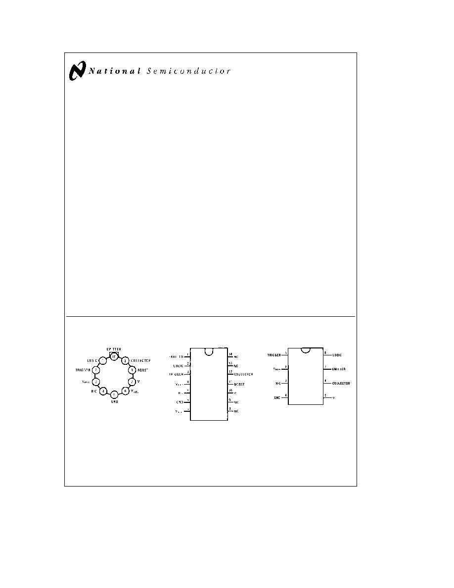
Connection Diagrams
Metal Can Package
TL H 7768 ≠ 6
Top View
Order Number LM122H
See NS Package Number H10C
Dual-In-Line Package
TL H 7768 ≠ 7
Top View
Order Number LM322N
See NS Package Number N14A
Dual-In-Line Package
TL H 7768 ≠ 8
Top View
Order Number LM3905N
See NS Package Number N08E
C1995 National Semiconductor Corporation
RRD-B30M115 Printed in U S A
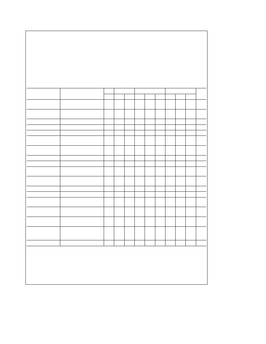
Absolute Maximum Ratings
If Military Aerospace specified devices are required
please contact the National Semiconductor Sales
Office Distributors for availability and specifications
Power Dissipation
500 mW
V
a
Voltage
40V
Collector Output Voltage
40V
V
REF
Current
5 mA
Trigger Voltage
g
40V
V
ADJ
Voltage (Forced)
5V
Logic Reverse Voltage
5 5V
Output Short Circuit Duration (Note 1)
Lead Temperature
(Soldering 10 sec )
260 C
Operating Temperature Range
LM122
b
55 C
s
T
A
s
a
125 C
LM322
0 C
s
T
A
s
a
70 C
LM3905
0 C
s
T
A
s
a
70 C
Electrical Characteristics
(Note 2)
Parameter
Conditions
LM122
LM322
LM3905
Units
Min
Typ
Max
Min
Typ
Max
Min
Typ
Max
Timing Ratio
T
A
e
25 C 4 5V
s
V
a s
40V 0 626 0 632 0 638 0 620 0 632 0 644 0 620 0 632 0 644
Boost Tied to V
a
(Note 3)
0 620 0 632 0 644 0 620 0 632 0 644
Comparator Input
T
A
e
25 C 4 5V
s
V
a s
40V
0 3
1 0
0 3
1 5
0 5
1 5
nA
Current
Boost Tied to V
a
30
100
30
100
nA
Trigger Voltage
T
A
e
25 C 4 5V
s
V
a s
40V
1 2
1 6
2
1 2
1 6
2
1 2
1 6
2
V
Trigger Current
T
A
e
25 C V
TRIG
e
2V
25
25
25
m
A
Supply Current
T
A
t
25 C 4 5V
s
V
a s
40V
2 5
4
2 5
4 5
2 5
4 5
mA
Timing Ratio
4 5V
s
V
a s
40V
0 62
0 644
0 61
0 654
0 61
0 654
Boost Tied to V
a
0 62
0 644
0 61
0 654
Comparator Input
4 5V
s
V
a s
40V
b
5
5
b
2
2
b
2 5
2 5
nA
Current
Boost Tied to V
a
(Note 4)
100
150
nA
Trigger Voltage
4 5V
s
V
a s
40V
0 8
2 5
0 8
2 5
0 8
2 5
V
Trigger Current
V
TRIG
e
2 5V
200
200
200
m
A
Output Leakage
V
CE
e
40V
1
5
5
m
A
Current
Capacitor Saturation
R
t
t
1 MX
2 5
2 5
2 5
mV
Voltage
R
t
e
10 kX
25
25
25
mV
Reset Resistance
150
150
150
X
Reference Voltage
T
A
e
25 C
3
3 15
3 3
3
3 15
3 3
3
3 15
3 3
V
Reference Regulation
0
s
I
OUT
s
3 mA
20
50
20
50
20
50
mV
4 5V
s
V
a s
40V
6
25
6
25
6
25
mV
Collector Saturation
I
L
e
8 mA
0 25
0 4
0 25
0 4
0 25
0 4
V
Voltage
I
L
e
50 mA
0 7
1 4
0 7
1 4
0 7
1 4
V
Emitter Saturation
T
A
e
25 C I
L
e
3 mA
1 8
2 2
1 8
2 2
1 8
2 2
V
Voltage
T
A
e
25 C I
L
e
50 mA
2 1
3
2 1
3
2 1
3
V
Average Temperature
Coefficient of Timing
0 003
0 003
0 003
% C
Ratio
Minimum Trigger Width V
TRIG
e
3V
0 25
0 25
0 25
m
s
Note 1
Continuous output shorts are not allowed Short circuit duration at ambient temperatures up to 40 C may be calculated from t
e
120 V
CE
seconds where
V
CE
is the collector to emitter voltage across the output transistor during the short
Note 2
These specifications apply for T
AMIN
s
T
A
s
T
AMAX
unless otherwise noted
Note 3
Output pulse width can be calculated from the following equation t
e
(R
t
) (C
t
) 1
b
2(0 632
b
r)
b
V
C
V
REF
) where r is timing ratio and V
C
is capacitor
saturation voltage This reduces to t
e
(R
t
) (C
t
) for all but the most critical applications
Note 4
Sign reversal may occur at high temperatures (
l
100 C) where comparator input current is predominately leakage See typcial curves
Note 5
Refer to RETS122X drawing of military LM122H version for specifications
2
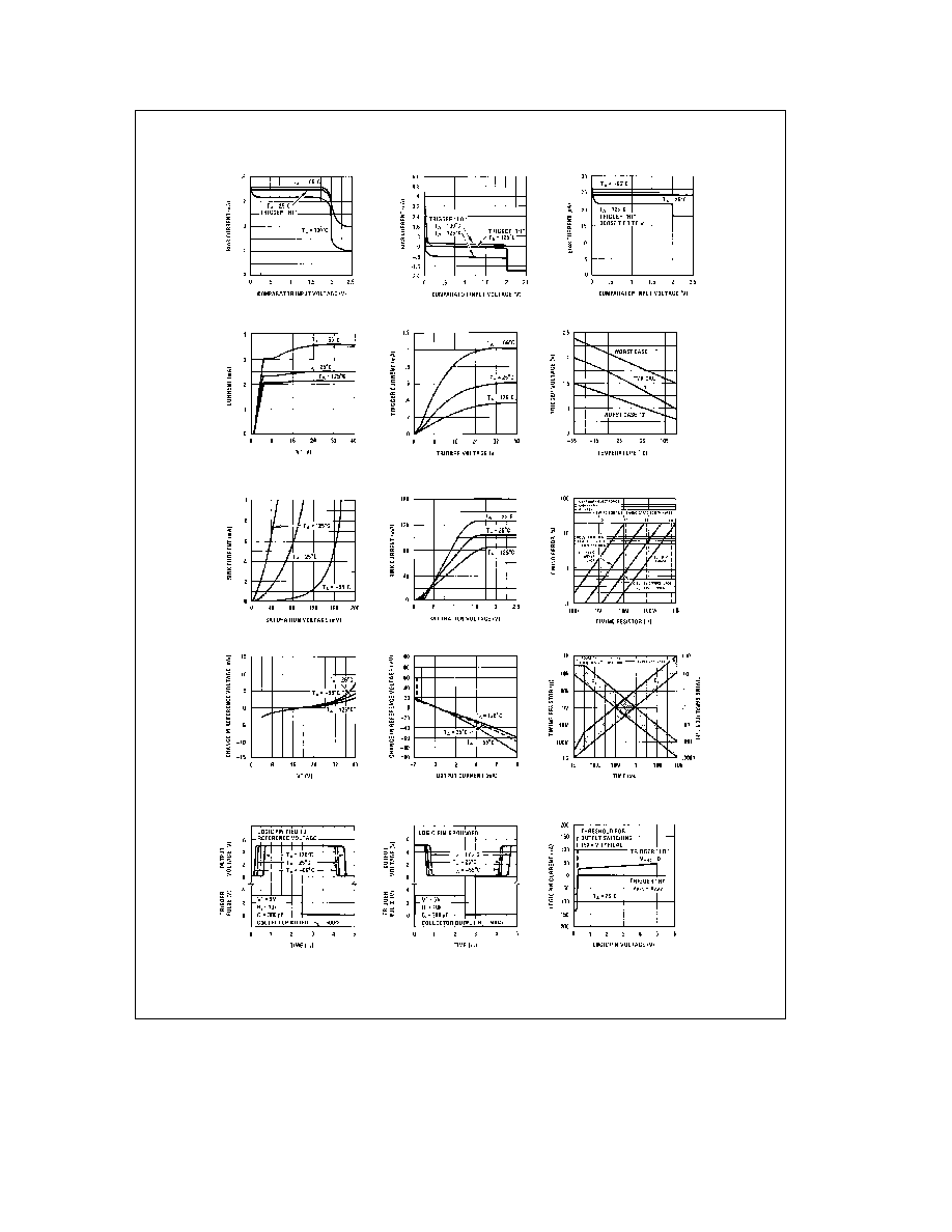
Typical Performance Characteristics
Comparator Bias Current
Comparator Bias Current
(LM122 LM322)
Comparator Bias Current
TL H 7768 ≠ 3
Supply Current
Trigger Input Characteristics
Trigger Threshold
Characteristics at Low Currents
Output Transistor Saturation
Characteristics at High Current
Collector Output Saturation
Comparator Bias Current
Timing Error Due to
Reference Regulation
Reference Regulation
Suggested Timing Components
(LM122 LM322)
Short Output Pulse
(LM122 LM322)
Short Output Pulse
Logic Pin Characteristics
TL H 7768 ≠ 4
3
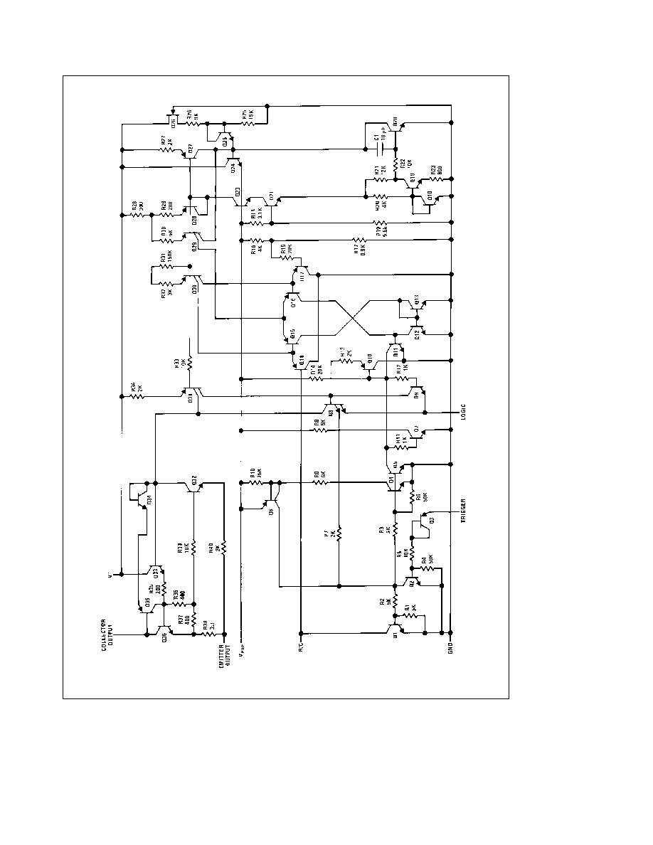
Schematic Diagram
TLH7768
≠
5
4
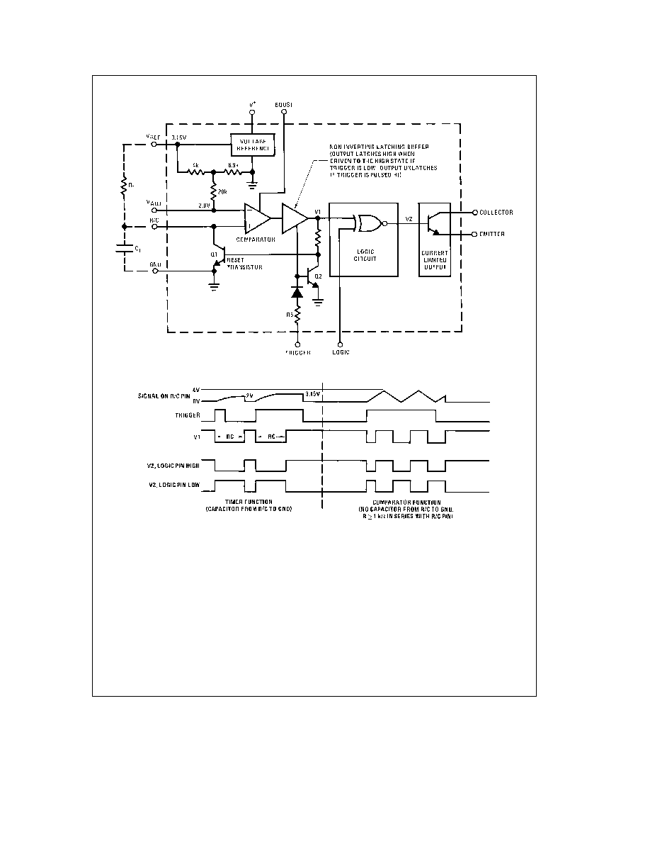
Functional Diagram
TL H 7768 ≠ 9
Timing Diagram
TL H 7768 ≠ 10
Pin Function Description
One of the main features of the LM122 is its great versatility
Since this device is unique a description of the functions
and limitations of each pin is in order This will make it much
easier to follow the discussion of the various applications
presented in this note
V
a
is the positive supply terminal of the LM122 When us-
ing a single supply this terminal may be driven by any volt-
age between 4 5V and 40V The effect of supply variations
on timing period is less than 0 005% V so supplies with
high ripple content may be used without causing pulse width
changes Supply bypassing on V
a
is not generally needed
but may be necessary when driving highly reactive loads
Quiescent current drawn from the V
a
terminal is typically
2 5 mA independent of the supply voltage Of course addi-
tional current will be drawn if the reference is externally
loaded
The V
REF
pin is the output of a 3 15V series regulator refer-
enced to the ground pin Up to 5 0 mA can be drawn from
this pin for driving external networks In most applications
the timing resistor is tied to V
REF
but it need not be in
situations where a more linear charging current is required
The regulated voltage is very useful in applications where
the LM122 is not used as a timer such as switching regula-
tors variable reference comparators and temperature con-
5