 | ÐлекÑÑоннÑй компоненÑ: LM1247 | СкаÑаÑÑ:  PDF PDF  ZIP ZIP |
Äîêóìåíòàöèÿ è îïèñàíèÿ www.docs.chipfind.ru

LM1247
150 MHz I
2
C Compatible RGB Preamplifier with Internal
512 Character OSD ROM, 512 Character RAM and 4
DACs
General Description
The LM1247 pre-amp is an integrated CMOS CRT preamp.
It has an I
2
C compatible interface which allows control of all
the parameters necessary to directly setup and adjust the
gain and contrast in the CRT display. Brightness and bias
can be controlled through the DAC outputs which are well
matched to the LM2479 and LM2480 integrated bias clamp
ICs. The LM1247 preamp is also designed to be compatible
with the LM246x high gain driver family.
Black level clamping of the video signal is carried out directly
on the AC coupled input signal into the high impedance
preamplifier input, thus eliminating the need for additional
clamp capacitors. Horizontal and vertical blanking of the
outputs is provided. Vertical blanking is optional and its
duration is register programmable.
The IC is packaged in an industry standard 24 lead DIP
molded plastic package.
Features
n
Internal 512 character OSD ROM usable as either (a)
384 2-color plus 128 4-color characters, (b) 640 2-color
characters, or (c) some combination in between
n
Internal 512 character RAM, which can be displayed as
one single or two independent windows
n
I
2
C compatible microcontroller interface
n
OSD override allows OSD messages to override video
and the use of burn-in screens with no video input
n
4 DAC outputs (8-bit resolution) for bus controlled CRT
bias and brightness
n
Spot killer which blanks the video outputs when V
CC
falls below the specified threshold
n
Suitable for use with discrete or integrated clamp, with
software configurable brightness mixer
n
Horizontal blanking and OSD synchronization directly
from deflection signals. The blanking can be disabled, if
desired
n
Vertical blanking and OSD synchronization directly from
deflection signals. The blanking width is register
programmable and can be disabled, if desired
n
Power Saving Mode with 65% power reduction
n
Matched to LM246x driver and LM2479/80 bias IC's
Applications
n
Low end 15" and 17" bus controlled monitors with OSD
n
1024x768 displays up to 85 Hz requiring OSD capability
n
Very low cost systems with LM246x driver
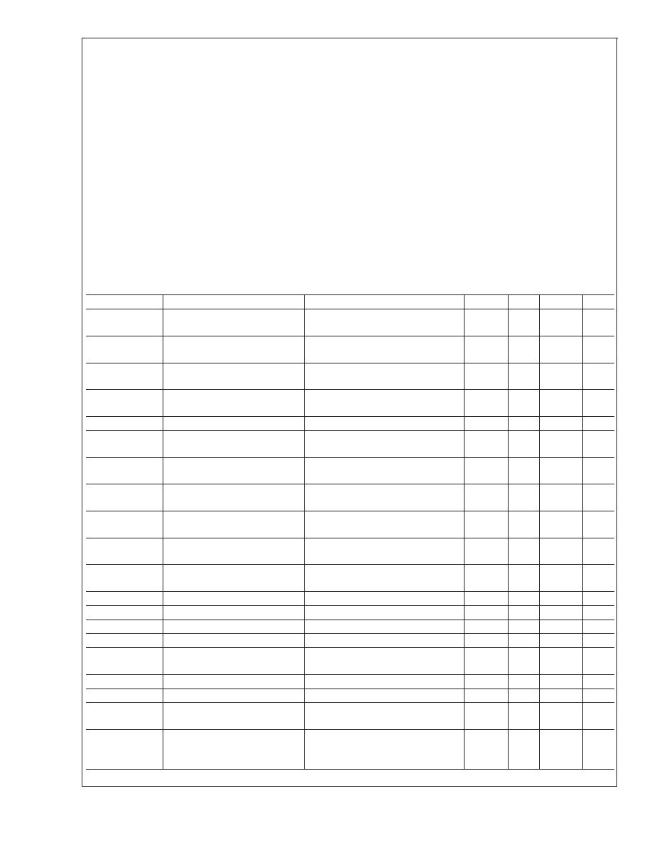
Internal Block Diagram
20048401
FIGURE 1. Order Number LM1247AAG/NA
See NS Package Number N24D
December 2002
LM1247
150
MHz
I
2
C
Compatible
RGB
Preamplifier
with
Internal
512
Character
OSD
ROM,
512
Character
RAM
and
4
DACs
© 2002 National Semiconductor Corporation
DS200484
www.national.com
Absolute Maximum Ratings
(Notes 1, 3)
If Military/Aerospace specified devices are required, please contact the National Semiconductor Sales Office/
Distributors for availability and specifications.
Supply Voltage V
CC
, Pins 10 and 18
6.0V
Peak Video DC Output Source Current
(Any One Amp) Pins 19, 20 or 21
1.5 mA
Voltage at Any Input Pin (V
IN
)
V
CC
+0.5
V
IN
-0.5V
Video Inputs (pk-pk)
0.0
V
IN
1.2V
Thermal Resistance to Ambient (
JA
)
51°C/W
Power Dissipation (P
D
)
(Above 25°C Derate Based
on
JA
and T
J
)
2.4W
Thermal Resistance to case (
JC
)
32°C/W
Junction Temperature (T
J
)
150°C
ESD Susceptibility (Note 4)
3.0 kV
ESD Machine Model (Note 13)
350V
Storage Temperature
-65°C to +150°C
Lead Temperature (Soldering, 10 sec.)
265°C
Operating Ratings
(Note 2)
Temperature Range
0°C to +70°C
Supply Voltage V
CC
4.75V
V
CC
5.25V
Video Inputs (pk-pk)
0.0V
V
IN
1.0V
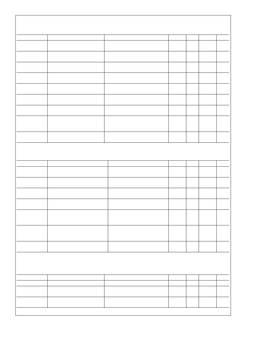
Video Signal Electrical Characteristics
Unless otherwise noted: T
A
= 25°C, V
CC
= +5.0V, V
IN
= 0.70 V
P-P
, V
ABL
= V
CC
, C
L
= 8 pF, Video Outputs = 2.0 V
P-P
. Setting
numbers refer to the definitions in Table 1. See (Note 7) for Min and Max parameters and (Note 6) for Typicals.
Symbol
Parameter
Conditions
Min
Typ
Max
Units
I
S
Supply Current
Test Setting 1, both supplies, no
output loading. See (Note 8).
195
250
mA
I
S-PS
Supply Current, Power Save
Mode
Test Setting 1, both supplies, no
output loading. See (Note 8).
55
85
mA
V
O BLK
Active Video Black Level Output
Voltage
Test Setting 4, no AC input signal, DC
offset (register 0x8438 set to 0xd5).
1.2
VDC
V
O BLK STEP
Active Video Black Level Step
Size
Test Setting 4, no AC input signal.
100
mVDC
V
O
Max
Maximum Video Output Voltage
Test Setting 3, Video in = 0.70 V
P-P
4.0
4.3
V
LE
Linearity Error
Test Setting 4, staircase input signal
(see (Note 9)).
5
%
t
r
Video Rise Time
(Note 5), 10% to 90%, Test Setting 4,
AC input signal.
3.1
ns
OS
R
Rising Edge Overshoot
(Note 5), Test Setting 4, AC input
signal.
2
%
t
f
Video Fall Time
(Note 5), 90% to 10%, Test Setting 4,
AC input signal.
2.9
ns
OS
F
Falling Edge Overshoot
(Note 5), Test Setting 4, AC input
signal.
2
%
BW
Channel bandwidth (-3 dB)
(Note 5), Test Setting 4, AC input
signal.
150
MHz
V
SEP
10 kHz
Video Amplifier 10 kHz Isolation
(Note 14), Test Setting 8.
-60
dB
V
SEP
10 MHz
Video Amplifier 10 MHz Isolation
(Note 14), Test Setting 8.
-50
dB
A
V
Max
Maximum Voltage Gain
Test Setting 8, AC input signal.
3.8
4.1
V/V
A
V
C-50%
Contrast Attenuation
@
50%
Test Setting 5, AC input signal.
-5.2
dB
A
V
Min/A
V
Max
Maximum Contrast Attenuation
(dB)
Test Setting 2, AC input signal.
-20
dB
A
V
G-50%
Gain Attenuation
@
50%
Test Setting 6, AC input signal.
-4.0
dB
A
V
G-Min
Maximum Gain Attenuation
Test Setting 7, AC input signal.
-11
dB
A
V
Match
Maximum Gain Match between
channels
Test Setting 3, AC input signal.
±
0.5
dB
A
V
Track
Gain Change between channels
Tracking when changing from Test
Setting 8 to Test Setting 5. See (Note
11).
±
0.5
dB
LM1247
www.national.com
2
Video Signal Electrical Characteristics
(Continued)
Unless otherwise noted: T
A
= 25°C, V
CC
= +5.0V, V
IN
= 0.70 V
P-P
, V
ABL
= V
CC
, C
L
= 8 pF, Video Outputs = 2.0 V
P-P
. Setting
numbers refer to the definitions in Table 1. See (Note 7) for Min and Max parameters and (Note 6) for Typicals.
Symbol
Parameter
Conditions
Min
Typ
Max
Units
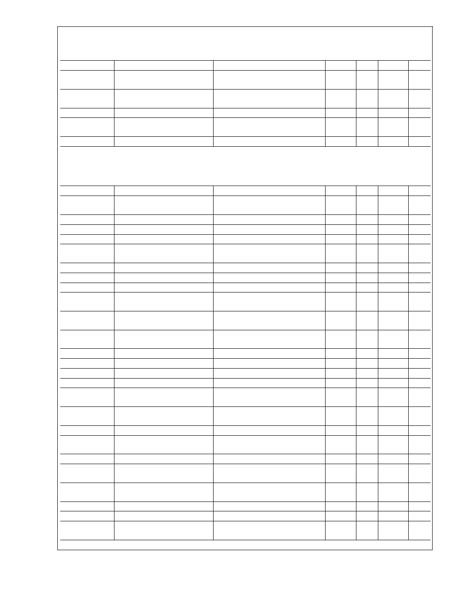
V
ABL
TH
ABL Control Range upper limit
(Note 12), Test Setting 4, AC input
signal.
4.8
V
V
ABL
Range
ABL Gain Reduction Range
(Note 12), Test Setting 4, AC input
signal.
2.8
V
A
V 3.5
/A
V Max
ABL Gain Reduction at 3.5V
(Note 12), Test Setting 4, AC input
signal. V
ABL
= 3.5V
-2
dB
A
V 2.0
/A
V Max
ABL Gain Reduction at 2.0V
(Note 12), Test Setting 4, AC input
signal. V
ABL
= 2.0V
-12
dB
I
ABL
Active
ABL Input bias current during
ABL
(Note 12), Test Setting 4, AC input
signal. V
ABL
= V
ABL
MIN GAIN
10
µA
I
ABL
Max
ABL input current sink capability
(Note 12), Test Setting 4, AC input
signal.
1.0
mA
V
ABL
Max
Maximum ABL Input voltage
during clamping
(Note 12), Test Setting 4, AC input
signal. I
ABL
= I
ABL
MAX
V
CC
+
0.1
V
A
V
ABL Track
ABL Gain Tracking Error
(Note 9), Test Setting 4, 0.7 V
P-P
input signal, ABL voltage set to 4.5V
and 2.5V.
4.5
%
R
IP
Minimum Input resistance (pins 5,
6, 7)
Test Setting 4.
20
M
OSD Electrical Characteristics
Unless otherwise noted: T
A
= 25°C, V
CC
= +5.0V. See (Note 7) for Min and Max parameters and (Note 6) for Typicals.
Symbol
Parameter
Conditions
Min
Typ
Max
Units
V
OSDHIGH
max
Maximum OSD Level with OSD
Contrast 11
Palette Set at 111, OSD Contrast =
11, Test Setting 3
4.5
V
V
OSDHIGH
10
Maximum OSD Level with OSD
Contrast 10
Palette Set at 111, OSD Contrast =
10, Test Setting 3
3.9
V
V
OSDHIGH
01
Maximum OSD Level with OSD
Contrast 01
Palette Set at 111, OSD Contrast =
01, Test Setting 3
3.2
V
V
OSDHIGH
00
Maximum OSD Level with OSD
Contrast 00
Palette Set at 111, OSD Contrast =
00, Test Setting 3
2.4
V
V
OSD
(Black)
Difference between OSD Black
Level and Video Black Level (same
channel)
Register 08=0x18, Input Video =
Black, Same Channel, Test Setting
8
20
mV
V
OSD
(White)
Output Match between Channels
Palette Set at 111, OSD Contrast =
11, Maximum difference between R,
G and B
3
%
V
OSD-out
(Track)
Output Variation between Channels OSD contrast varied from max to
min
3
%
DAC Output Electrical Characteristics
Unless otherwise noted: T
A
= 25°C, V
CC
= +5.0V, V
IN
= 0.7V, V
ABL
= V
CC
, C
L
= 8 pF, Video Outputs = 2.0 V
P-P
. See (Note 7)
for Min and Max parameters and (Note 6) for Typicals. DAC parameters apply to all 4 DACs.
Symbol
Parameter
Conditions
Min
Typ
Max
Units
V
Min DAC
Min output voltage of DAC
Register Value = 0x00
0.5
0.7
V
V
Max DAC
Mode 00
Max output voltage of DAC
Register Value = 0xFF,
DCF[1:0] = 00b
3.7
4.2
V
V
Max DAC
Mode 01
Max output voltage of DAC in
DCF mode 01
Register Value = 0xFF,
DCF[1:0] = 01b
1.85
2.35
V
LM1247
www.national.com
3
DAC Output Electrical Characteristics
(Continued)
Unless otherwise noted: T
A
= 25°C, V
CC
= +5.0V, V
IN
= 0.7V, V
ABL
= V
CC
, C
L
= 8 pF, Video Outputs = 2.0 V
P-P
. See (Note 7)
for Min and Max parameters and (Note 6) for Typicals. DAC parameters apply to all 4 DACs.
Symbol
Parameter
Conditions
Min
Typ
Max
Units
V
Max DAC
(Temp)
Variation in voltage of DAC with
temperature
0
<
T
<
70°C ambient
±
0.5
mV/°C
V
Max DAC
(V
CC
)
DAC output voltage variation with
V
CC
V
CC
varied from 4.75V to 5.25V, DAC
register set to mid-range (0x7F)
50
mV
Linearity
Linearity of DAC over its range
5
%
Monotonicity
Monotonicity of the DAC
Excluding dead zones
±
0.5
LSB
I
MAX
Max Load Current
-1.0
1.0
mA
System Interface Signal Characteristics
Unless otherwise noted: T
A
= 25°C, V
CC
= +5.0V, V
IN
= 0.7V, V
ABL
= V
CC
, C
L
= 8 pF, Video Outputs = 2.0 V
P-P
. See (Note 7)
for Min and Max parameters and (Note 6) for Typicals. DAC parameters apply to all 4 DACs.
Symbol
Parameter
Conditions
Min
Typ
Max
Units
V
VTH+
VFLYBACK positive switching
guarantee
Vertical Blanking triggered
2.0
V
V
SPOT
Spot Killer Voltage
(Note 17), V
CC
Adjusted to Activate
3.4
3.9
4.3
V
V
Ref
V
Ref
Output Voltage (pin 2)
1.25
1.45
1.65
V
V
IL
(SCL, SDA)
Logic Low Input Voltage
-0.5
1.5
V
V
IH
(SCL, SDA)
Logic High Input Voltage
3.0
V
CC
+
0.5
V
I
L
(SCL, SDA)
Logic Low Input Current
SDA or SCL, Input Voltage = 0.4V
±
10
µA
I
H
(SCL, SDA)
Logic High Input Voltage
SDA or SCL, Input Voltage = 4.5V
±
10
µA
V
OL
(SCL, SDA)
Logic Low Output Voltage
I
O
= 3 mA
0.5
V
f
H
Min
Minimum Horizontal Frequency
PLL & OSD Operational; PLL Range
= 0
25
kHz
f
H
Max
Maximum Horizontal Frequency
PLL & OSD Operational; PLL Range
= 3
110
kHz
I
HFB IN
Max
Horizontal Flyback Input
Current Absolute Maximum During
Flyback
5
mA
I
IN
Peak Current during flyback
Design Value
4
mA
I
HFB OUT
Max
Horizontal Flyback Input Current
Absolute Maximum During Scan
-700
µA
I
OUT
Peak Current during Scan
Not exact - Duty Cycle Dependent
-550
µA
I
IN THRESHOLD
I
IN
H-Blank Detection Threshold
0
µA
t
H-BLANK ON
H-Blank Time Delay - On
+ Zero crossing of I
HFB
to 50% of
output blanking start. I
24
= +1.5mA
45
ns
t
H-BLANK OFF
H-Blank Time Delay - Off
- Zero crossing of I
HFB
to 50% of
output blanking end. I
24
= -100µA
85
ns
V
BLANK
Max
Maximum Video Blanking Level
Test Setting 4, AC input signal
0
0.25
V
f
FREERUN
Free Run H Frequency, including
H Blank
42
kHz
t
PW CLAMP
Minimum Clamp Pulse Width
See (Note 15)
200
ns
V
CLAMP MAX
Maximum Low Level Clamp
Pulse Voltage
Video Clamp Functioning
2.0
V
V
CLAMP MIN
Minimum High Level Clamp
Pulse Voltage
Video Clamp Functioning
3.0
V
I
CLAMP
Low
Clamp Gate Low Input Current
V
23
= 2V
-0.4
µA
I
CLAMP
High
Clamp Gate High Input Current
V
23
= 3V
0.4
µA
t
CLAMP-VIDEO
Time from End of Clamp Pulse to
Start of Video
Referenced to Blue, Red and Green
inputs
50
ns
LM1247
www.national.com
4
System Interface Signal Characteristics
(Continued)
Note 1: Limits of Absolute Maximum Ratings indicate below which damage to the device must not occur.
Note 2: Operating ratings indicate conditions for which the device is functional, but do not guarantee specific performance limits.
Note 3: All voltages are measured with respect to GND, unless otherwise specified.
Note 4: Human body model, 100 pF discharged through a 1.5 k
resistor.
Note 5: Input from signal generator: t
r
, t
f
<
1 ns.
Note 6: Typical specifications are specified at +25°C and represent the most likely parametric norm.
Note 7: Datasheet min/max specification limits are guaranteed by design, test, or statistical analysis. The guaranteed specifications apply only for the test conditions
listed. Some performance characteristics may change when the device is not operated under the listed test conditions.
Note 8: The supply current specified is the quiescent current for V
CC
and 5V Dig with R
L
=
. Load resistors are not required and are not used in the test circuit,
therefore all the supply current is used by the pre-amp.
Note 9: Linearity Error is the maximum variation in step height of a 16 step staircase input signal waveform with a 0.7 V
P-P
level at the input. All 16 steps equal,
with each at least 100 ns in duration.
Note 10: dt/dV
CC
= 200*(t
5.5V
t
4.5V
)/ ((t
5.5V
+ t
4.5V
)) %/V, where: t
5.5V
is the rise or fall time at V
CC
= 5.5V, and t
4.5V
is the rise or fall time at V
CC
= 4.5V.
Note 11:
A
V
track is a measure of the ability of any two amplifiers to track each other and quantifies the matching of the three gain stages. It is the difference in
gain change between any two amplifiers with the contrast set to A
V
C-50% and measured relative to the A
V
max condition. For example, at A
V
max the three
amplifiers' gains might be 12.1 dB, 11.9 dB, and 11.8 dB and change to 2.2 dB, 1.9 dB and 1.7 dB respectively for contrast set to A
V
C-50%. This yields a typical
gain change of 10.0 dB with a tracking change of
±
0.2 dB.
Note 12: The ABL input provides smooth decrease in gain over the operational range of 0 dB to -5 dB:
A
ABL
= A(V
ABL
= V
ABL MAX GAIN
) A (V
ABL
=
V
ABL MIN GAIN
). Beyond -5 dB the gain characteristics, linearity and pulse response may depart from normal values.
Note 13: Machine Model ESD test is covered by specification EIAJ IC-121-1981. A 200 pF cap is charged to the specific voltage, then discharged directly into the
IC with no external series resistor (resistance of discharge path must be under 50
).
Note 14: Measure output levels of the other two undriven amplifiers relative to the driven amplifier to determine channel separation. Terminate the undriven amplifier
inputs to simulate generator loading. Repeat test at f
IN
= 10 MHz for V
SEP
10 MHz.
Note 15: A minimum pulse width of 200 ns is the guaranteed minimum for a horizontal line of 15 kHz. This limit is guaranteed by design. If a lower line rate is used
then a longer clamp pulse may be required.
Note 16: Adjust input frequency from 10 MHz (A
V
max reference level) to the -3 dB corner frequency (f
-3 dB
).
Note 17: Once the spot killer has been activated, the LM1247 remains in the off state until V
CC
is cycled (reduced below 0.5V and then restored to 5V).
Hexadecimal and Binary Notation
Hexadecimal numbers appear frequently throughout this
document, representing slave and register addresses, and
register values. These appear in the format "0x...". For ex-
ample, the slave address for writing the registers of the
LM1247 is hexadecimal BA, written as 0xBA. On the other
hand, binary values, where the individual bit values are
shown, are indicated by a trailing "b". For example, 0xBA is
equal to 10111010b. A subset of bits within a register is
referred to by the bit numbers in brackets following the
register value. For example, the OSD contrast bits are the
fourth and fifth bits of register 0x8438. Since the first bit is bit
0, the OSD contrast register is 0x8438[4:3].
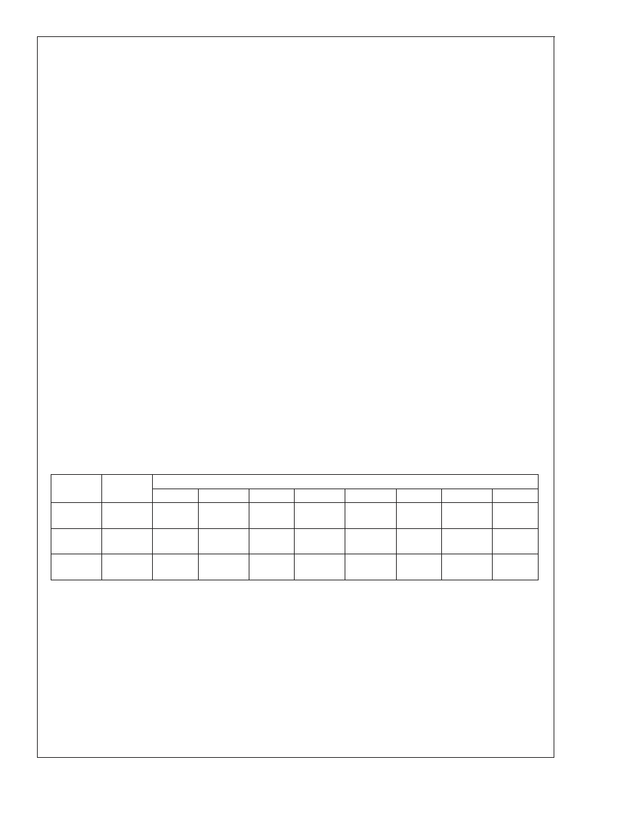
Register Test Settings
Table 1 shows the definitions of the Test Settings 18 re-
ferred to in the specifications sections. Each test setting is a
combination of five hexadecimal register values, Contrast,
Gain (Blue, Red, Green) and DC offset.
TABLE 1. Test Settings
Control
No. of Bits
Test Settings
1
2
3
4
5
6
7
8
Contrast
7
0x7F
(Max)
0x00
Min
0x7F
(Max)
0x7F
(Max)
0x40
(50.4%)
0x7F
(Max)
0x7F
(Max)
0x7F
(Max)
B, R, G
Gain
7
0x7F
(Max)
0x7F
(Max)
0x7F
(Max)
Set V
O
to
2 V
P-P
0x7F
(Max)
0x40
(50.4%)
0x00
(Min)
0x7F
(Max)
DC Offset
3
0x00
(Min)
0x05
0x07
(Max)
0x05
0x05
0x05
0x05
0x05
LM1247
www.national.com
5
Document Outline