LM1279
110 MHz RGB Video Amplifier System with OSD
General Description
The LM1279 is a full featured and low cost video amplifier
with OSD (On Screen Display). 8V operation for low power
and increased reliability. Supplied in a 20-pin DIP package,
accommodating very compact designs of the video channel
requiring OSD. All video functions controlled by 0V to 4V
high impedance DC inputs. This provides easy interfacing to
5V DACs used in computer controlled systems and digital
alignment systems. Unique OSD switching, no OSD switch-
ing signal required. An OSD signal at any OSD input typically
switches the LM1279 to the OSD mode within 5 ns. Ideal
video amplifier for the low cost OSD monitor with resolutions
up to 1280 x 1024. The LM1279 provides superior protection
against ESD. Excellent alternative for the MC13282 in new
designs.
Features
n
Three wideband video amplifiers 110 MHz
@
-3dB (4
V
PP
output)
n
OSD signal to any OSD input pin automatically switches
all 3 outputs to the OSD mode
n
Fast OSD switching time, typically 5 ns
n
3.5 kV ESD protection
n
Fixed cutoff level typically set to 1.35V
n
0V to 4V, high impedance DC contrast control with over
40 dB range
n
0V to 4V, high impedance DC drive control (0 dB to
-12 dB range)
n
Matched (
�
0.3 dB or 3.5%) attenuators for contrast
control
n
Output stage directly drives CRT drivers
n
Ideal combination with LM2407 CRT driver
Applications
n
High resolution RGB CRT monitors
n
Video AGC amplifiers
n
Wideband amplifiers with contrast and drive controls
n
Interface amplifiers for LCD or CCD systems
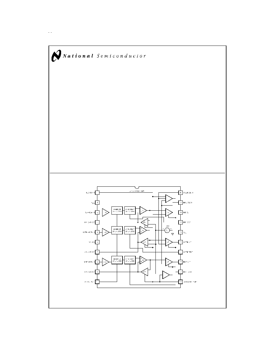
Block and Connection Diagram
DS100091-1
FIGURE 1. Order Number LM1279N
See NS Package Number N20A
September 1998
LM1279
1
1
0
MHz
RGB
V
ideo
Amplifier
System
with
OSD
� 1998 National Semiconductor Corporation
DS100091
www.national.com
Absolute Maximum Ratings
(Note 1)
If Military/Aerospace specified devices are required,
please contact the National Semiconductor Sales Office/
Distributors for availability and specifications.
Supply Voltage
Pins 2 and 16 (Note 3)
10V
Peak Video Output Source Current
(Any One Amp) Pins 13, 15, or 18
28 mA
Voltage at Any Input Pin (V
IN
)
V
CC
V
IN
GND
Power Dissipation (P
D
)
(Above 25�C Derate Based on
JA
and T
J
)
2.1W
Thermal Resistance to Ambient (
JA
)
60�C/W
Thermal Resistance to Case (
JA
)
37�C/W
Junction Temperature (T
J
)
150�C
ESD Susceptibility (Note 4)
3.5 kV
ESD Machine Model (Note 16)
300V
Storage Temperature
-65�C to 150�C
Lead Temperature
(Soldering, 10 sec.)
265�C
Operating Ratings
(Note 2)
Temperature Range
0�C to 70�C
Supply Voltage (V
CC
)
7.5V
V
CC
8.5V
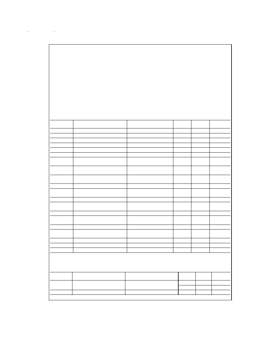
DC Electrical Characteristics
T
A
= 25�C; V
CC1
= V
CC2
= 8V; V
10
= 4V; V
Drive
= 4V; V
11
= 7V; V
OSD
= 0V; R
L
= 390
unless otherwise stated.
Symbol
Parameter
Condition
Typical
(Note 5)
Limit
(Note 6)
Units
I
S
Supply Current
I
CC1
+ I
CC2
- I
Load
(Note 7)
80
90
mA(max)
V
3, 5, 8
Video Amplifier Input Bias Voltage
2.5
V
R
IN
Video Input Resistance
Any One Amplifier
20
k
V
11off
Sandcastle Off Voltage
1.4
1.2
V (max)
V
11blank
Sandcastle Blank Voltage
Start of Blank Region
1.4
1.7
V (min)
V
11blank
Sandcastle Blank Voltage
End of Blank Region
2.8
3.2
V (max)
V
11clamp &
Blank
Sandcastle Clamp and Blank On
Voltage
Start of Clamp and Blank
Region
3.2
3.6
V (min)
V
11clamp &
Blank
Sandcastle Clamp and Blank On
Voltage
End of Clamp and Blank
Region
6.2
5.8
V (max)
V
11clamp
Sandcastle Clamp On/Blank Off
Voltage
Clamp Only Region, Max =
V
CC
6.2
6.5
V (min)
I
11off
Sandcastle Off Current
V
11
= 0V
-5.0
-8.0
�A(max)
I
11test
Sandcastle Clamp On/Blank Off
Curr
V
11
= 6.5V
-100
-500
nA(max)
I
clamp
Clamp Cap Charge Current
Clamp Comparators On
�
750
�
500
�A(min)
I
bias
Clamp Cap Bias Discharge
Current
Clamp Comparators Off
50
200
nA (max)
V
OL
Video Black Level
V
Video in
= 0V, V
11
= 6.5V
1.35
1.55
V (max)
V
OL
Video
Black Level Output
Voltage
Between Any Two Amplifiers
�
50
�
200
mV (max)
V
OH
Video Output High Voltage
V
11
<
1.2V
5.0
4.6
V (min)
I
10, 12, 14, 17
Contrast/Drive Control Input
Current
V
Contrast
= V
Drive
= 0V to 4V
-0.25
-1.5
�A (max)
I
1l, 19l, 20l
OSD Low Input Current (each)
V
OSD in
= 0V
-2.5
-10.0
�A(max)
I
1h, 19h, 20h
OSD High Input Current (each)
V
OSD in
= 5V
100
130
�A(max)
V
OL
(Blank)
Video Output during Blanking
V
11
= 1.7V
0.1
0.5
V (max)
AC Electical Characteristics
T
A
= 25�C; V
CC1
= V
CC2
= 8V. Manually adjust Video Output pins 13, 15, and 18 to 4V DC for the AC test unless otherwise
stated. (Note 15)
Symbol
Parameter
Conditions
Typical
(Note 5)
Limit
(Note 6)
Units
A
Vmax
Video Amplifier Gain
V
10
= 4V, V
IN
= 635 mV
PP
6.8
5.9
V/V (min)
V
drive
= 4V
16.7
15.4
dB (min)
A
V 2V
Contrast Attenuation
@
2V
Ref: A
V
max, V
10
= 2V
-6
dB
www.national.com
2
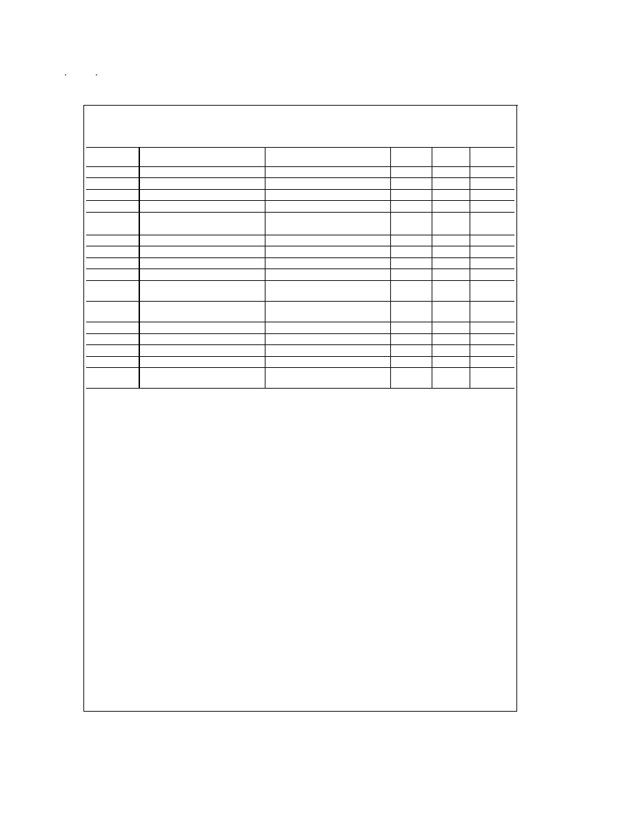
AC Electical Characteristics
(Continued)
T
A
= 25�C; V
CC1
= V
CC2
= 8V. Manually adjust Video Output pins 13, 15, and 18 to 4V DC for the AC test unless otherwise
stated. (Note 15)
Symbol
Parameter
Conditions
Typical
(Note 5)
Limit
(Note 6)
Units
A
V 0.25V
Contrast Attenuation
@
0V
Ref: A
V
max, V
10
= 0V
-35
dB
Drive
Drive Control Range
V
drive
= 0V to 4V, V
10
= 4V
12
dB
A
V match
Absolute Gain Match
@
A
V
max
V
10
= 4V, V
drive
= 4V (Note 9)
�
0.3
dB
A
V track
Gain Change Between Amplifiers
V
10
= 4V to 2V (Notes 9, 10)
�
0.3
dB
f(-3 dB)
Video Amplifier Bandwidth
V
10
= 4V, V
drive
= 4V,
110
MHz
(Notes 11, 12))
V
O
= 3.5 V
P-P
t
r
(Video)
Video Output Rise Time
V
O
= 3.5 V
P-P
(Note 11)
3.6
ns
t
f
(Video)
Video Output Fall Time
V
O
= 3.5 V
P-P
(Note 11)
3.2
ns
V
sep
10 kHz
Video Amplifier 10 kHz Isolation
V
10
= 4V (Note 13)
-70
dB
V
sep
10 MHz
Video Amplifier 10 MHz Isolation
V
10
= 4V (Notes 11, 13)
-50
dB
V
OL
(OSD)
OSD Black Level, Difference from
Video Black Level
V
OSD in
= 0.8V, OSD Mode
-0.4
-0.7
V (max)
V
OH
(OSD)
OSD Output High Voltage (above
measured video black level)
V
OSD in
= 2.5V, OSD Mode
2.1
2.4
V (max)
t
r
(OSD)
Going into OSD Mode
OSD Mode (
Figure 2)
5.0
ns
t
f
(OSD)
Going out of OSD Mode
OSD Mode (
Figure 2)
10.0
ns
t
r-prop
(OSD)
Starting OSD Propagation Delay
Switching to OSD Mode (
Figure 3)
13.0
ns
t
f-prop
(OSD)
Ending OSD Propagation Delay
Switching to Vid. Mode (
Figure 3)
14.0
ns
T
pw
(Clamp)
Input Clamp Pulse Width (Part of
Sandcastle Sync)
(Note 14)
200
ns (min)
Note 1: Absolute Maximum Ratings indicate limits beyond which damage to the device may occur.
Note 2: Operating Ratings indicate conditions for which the device is functional, but do not guarantee specific performance limits. For guaranteed specifications and
test conditions, see the Electrical Characteristics. The guaranteed specifications apply only for the test conditions listed. Some performance characteristics may de-
grade when the device is not operated under the listed test conditions.
Note 3: V
CC
supply pins 2 and 16 must be externally wired together to prevent internal damage during V
CC
power on/off cycles.
Note 4: Human body model, 100 pF discharged through a 1.5 k
resistor.
Note 5: Typical specifications are specified at +25�C and represent the most likely parametric norm.
Note 6: Tested limits are guaranteed to National's AOQL (Average Outgoing Quality Level).
Note 7: The supply current specified is the current for V
CC1
and V
CC2
minus the current through R
L
(I
supply
= I
CC1
+ I
CC2
- I
L
). The supply current for V
CC2
(pin 16)
does depend on the output load. With video output at 1V DC, the additional current through V
CC2
is 7.7 mA with R
L
= 390
.
Note 8: Output voltage is dependent on load resistor. Test circuit uses R
L
= 390
.
Note 9: Measure gain difference between any two amplifiers. V
IN
= 635 mV
PP
.
Note 10:
A
V
track is a measure of the ability of any two amplifiers to track each other and quantifies the matching of the three attenuators. It is the difference in
gain change between any two amplifiers with the contrast voltage (V
10
) at either 4V or 2V measured relative to an A
V
max condition, V
10
= 4V. For example, at A
V
max the three amplifiers' gains might be 17.1 dB, 16.9 dB, and 16.8 dB and change to 11.2 dB, 10.9 dB and 10.7 dB respectively for V
10
= 2V. This yields the mea-
sured typical
�
0.1 dB channel tracking.
Note 11: When measuring video amplifier bandwidth or pulse rise and fall times, a double sided full ground plane printed circuit board without socked is recom-
mended. Video amplifier 10 MHz isolation test also requires this printed circuit board. The reason for a double sided full ground plane PCB is that large measurement
variations occur in single sided PCBs.
Note 12: Adjust input frequency from 10 MHz (A
V
max reference level) to the -3 dB corner frequency (f
-3 dB
).
Note 13: Measure output levels of the other two undriven amplifiers relative to the driven amplifier to determine channel separation. Terminate the undriven amplifier
inputs to simulate generator loading. Repeat test at f
IN
= 10 MHz for V
sep
10 MHz.
Note 14: A minimum pulse width of 200 ns is guaranteed for a horizontal line of 15 kHz. This limit is guaranteed by design. If a lower line rate is used then a longer
clamp pulse may be required.
Note 15: During the AC test the 4V DC level is the center voltage of the AC output signal. For example, if the output is 4 V
PP
the signal will swing between 2V DC
and 6V DC.
Note 16: Machine Model ESD test is covered by specification EIAJ IC-121-1981. A 200 pF cap is charged to the specified voltage, then discharged directly into the
IC with no external series resistor (resistance of discharge path must be under 50
).
www.national.com
3
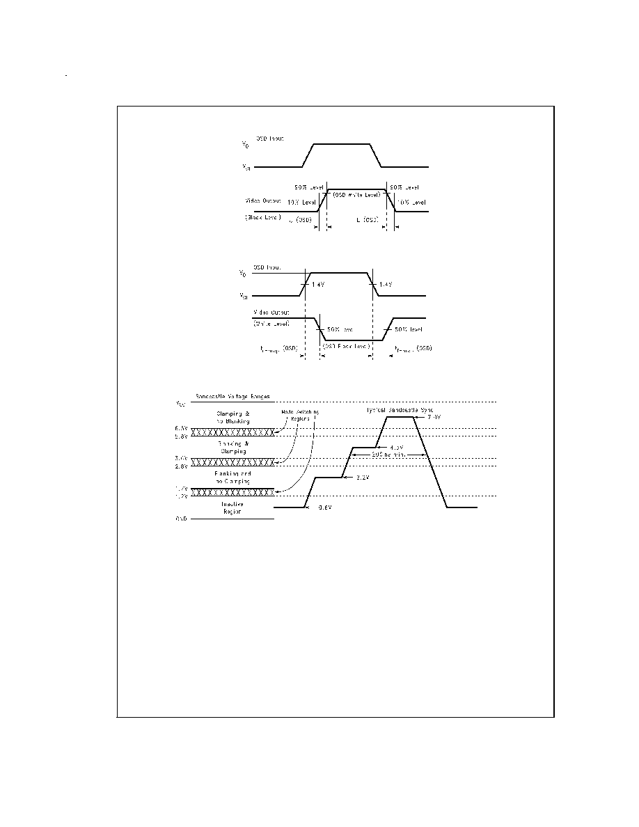
Timing Diagrams
DS100091-2
FIGURE 2. OSD Rise and Fall Times
DS100091-3
FIGURE 3. OSD Propagation Delays
DS100091-4
FIGURE 4. Sandcastle Sync Pulse
www.national.com
4
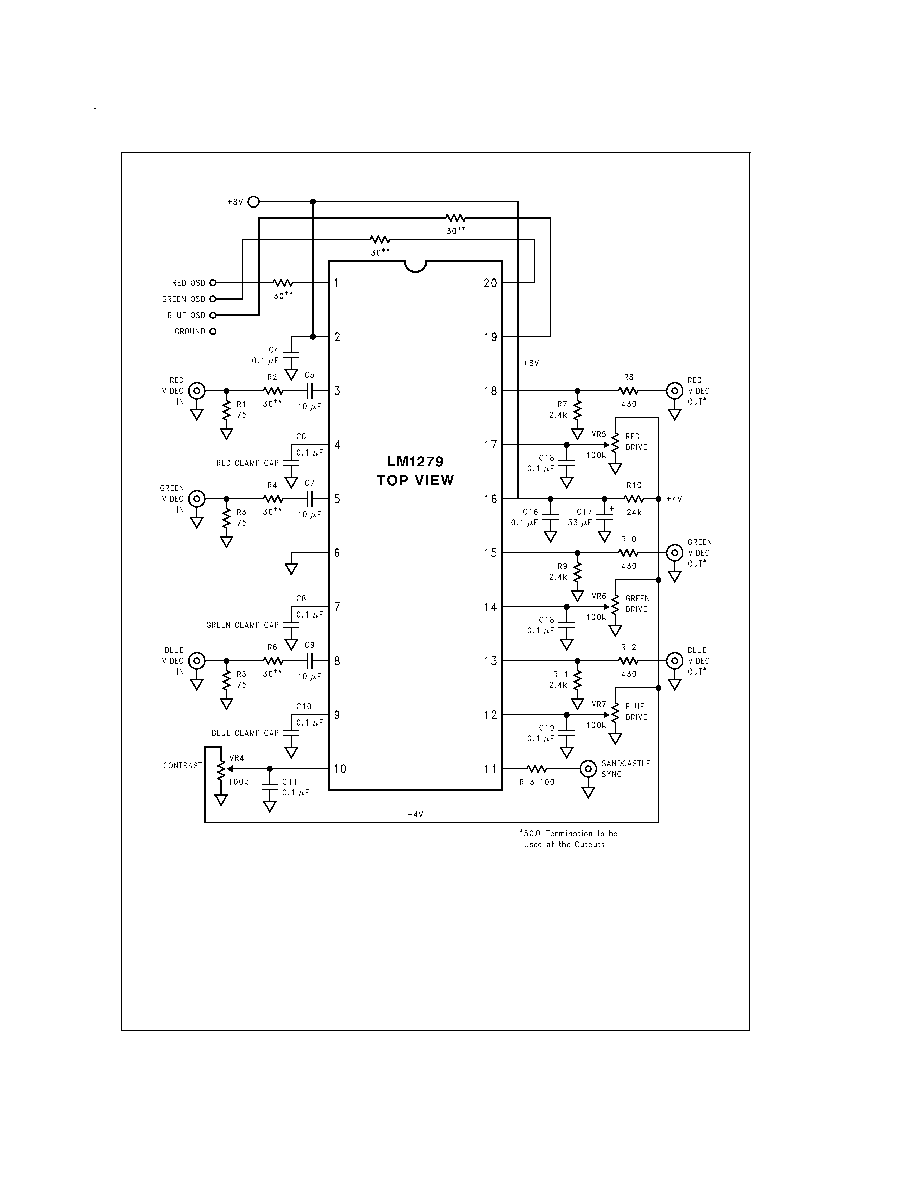
Test Circuits
DS100091-5
**Note: All video inputs
must have a series 30
resistor for protection against EOS (Electrical Over Stress). If the OSD signals are external to the monitor, or
these signals are present any time when +8V is not fully powered up, then the OSD inputs also
require a series 30
resistor.
FIGURE 5. LM1279 OSD Video Pre-amp Demonstration Board Schematic
www.national.com
5