 | –≠–ª–µ–∫—Ç—Ä–æ–Ω–Ω—ã–π –∫–æ–º–ø–æ–Ω–µ–Ω—Ç: LM1279N | –°–∫–∞—á–∞—Ç—å:  PDF PDF  ZIP ZIP |
LM1279
110 MHz RGB Video Amplifier System with OSD
General Description
The LM1279 is a full featured and low cost video amplifier
with OSD (On Screen Display). 8V operation for low power
and increased reliability. Supplied in a 20-pin DIP package,
accommodating very compact designs of the video channel
requiring OSD. All video functions controlled by 0V to 4V
high impedance DC inputs. This provides easy interfacing to
5V DACs used in computer controlled systems and digital
alignment systems. Unique OSD switching, no OSD switch-
ing signal required. An OSD signal at any OSD input typically
switches the LM1279 to the OSD mode within 5 ns. Ideal
video amplifier for the low cost OSD monitor with resolutions
up to 1280 x 1024. The LM1279 provides superior protection
against ESD. Excellent alternative for the MC13282 in new
designs.
Features
n
Three wideband video amplifiers 110 MHz
@
-3dB (4
V
PP
output)
n
OSD signal to any OSD input pin automatically switches
all 3 outputs to the OSD mode
n
Fast OSD switching time, typically 5 ns
n
3.5 kV ESD protection
n
Fixed cutoff level typically set to 1.35V
n
0V to 4V, high impedance DC contrast control with over
40 dB range
n
0V to 4V, high impedance DC drive control (0 dB to
-12 dB range)
n
Matched (
±
0.3 dB or 3.5%) attenuators for contrast
control
n
Output stage directly drives CRT drivers
n
Ideal combination with LM2407 CRT driver
Applications
n
High resolution RGB CRT monitors
n
Video AGC amplifiers
n
Wideband amplifiers with contrast and drive controls
n
Interface amplifiers for LCD or CCD systems
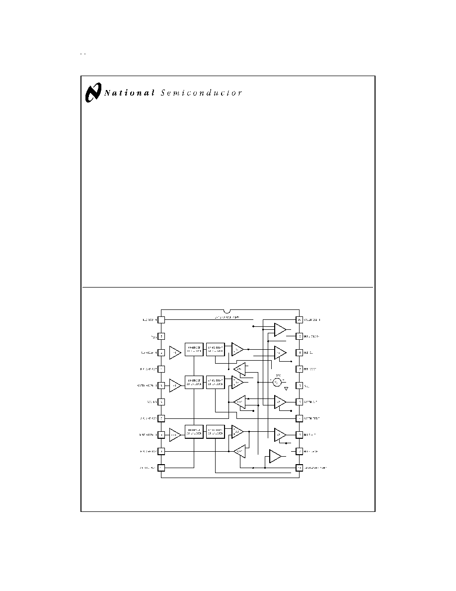
Block and Connection Diagram
DS100091-1
FIGURE 1. Order Number LM1279N
See NS Package Number N20A
September 1998
LM1279
1
1
0
MHz
RGB
V
ideo
Amplifier
System
with
OSD
© 1998 National Semiconductor Corporation
DS100091
www.national.com
Absolute Maximum Ratings
(Note 1)
If Military/Aerospace specified devices are required,
please contact the National Semiconductor Sales Office/
Distributors for availability and specifications.
Supply Voltage
Pins 2 and 16 (Note 3)
10V
Peak Video Output Source Current
(Any One Amp) Pins 13, 15, or 18
28 mA
Voltage at Any Input Pin (V
IN
)
V
CC
V
IN
GND
Power Dissipation (P
D
)
(Above 25∞C Derate Based on
JA
and T
J
)
2.1W
Thermal Resistance to Ambient (
JA
)
60∞C/W
Thermal Resistance to Case (
JA
)
37∞C/W
Junction Temperature (T
J
)
150∞C
ESD Susceptibility (Note 4)
3.5 kV
ESD Machine Model (Note 16)
300V
Storage Temperature
-65∞C to 150∞C
Lead Temperature
(Soldering, 10 sec.)
265∞C
Operating Ratings
(Note 2)
Temperature Range
0∞C to 70∞C
Supply Voltage (V
CC
)
7.5V
V
CC
8.5V
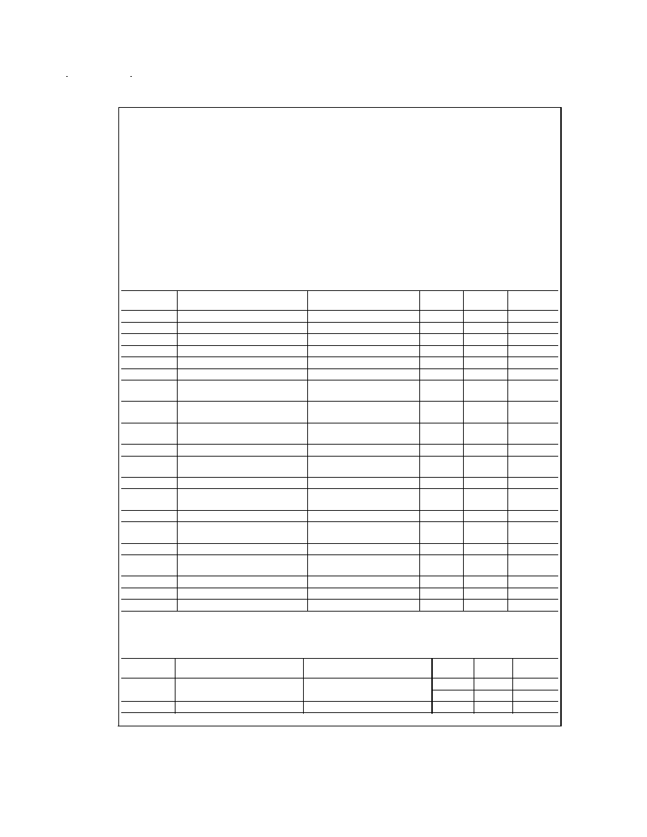
DC Electrical Characteristics
T
A
= 25∞C; V
CC1
= V
CC2
= 8V; V
10
= 4V; V
Drive
= 4V; V
11
= 7V; V
OSD
= 0V; R
L
= 390
unless otherwise stated.
Symbol
Parameter
Condition
Typical
(Note 5)
Limit
(Note 6)
Units
I
S
Supply Current
I
CC1
+ I
CC2
- I
Load
(Note 7)
80
90
mA(max)
V
3, 5, 8
Video Amplifier Input Bias Voltage
2.5
V
R
IN
Video Input Resistance
Any One Amplifier
20
k
V
11off
Sandcastle Off Voltage
1.4
1.2
V (max)
V
11blank
Sandcastle Blank Voltage
Start of Blank Region
1.4
1.7
V (min)
V
11blank
Sandcastle Blank Voltage
End of Blank Region
2.8
3.2
V (max)
V
11clamp &
Blank
Sandcastle Clamp and Blank On
Voltage
Start of Clamp and Blank
Region
3.2
3.6
V (min)
V
11clamp &
Blank
Sandcastle Clamp and Blank On
Voltage
End of Clamp and Blank
Region
6.2
5.8
V (max)
V
11clamp
Sandcastle Clamp On/Blank Off
Voltage
Clamp Only Region, Max =
V
CC
6.2
6.5
V (min)
I
11off
Sandcastle Off Current
V
11
= 0V
-5.0
-8.0
µA(max)
I
11test
Sandcastle Clamp On/Blank Off
Curr
V
11
= 6.5V
-100
-500
nA(max)
I
clamp
Clamp Cap Charge Current
Clamp Comparators On
±
750
±
500
µA(min)
I
bias
Clamp Cap Bias Discharge
Current
Clamp Comparators Off
50
200
nA (max)
V
OL
Video Black Level
V
Video in
= 0V, V
11
= 6.5V
1.35
1.55
V (max)
V
OL
Video
Black Level Output
Voltage
Between Any Two Amplifiers
±
50
±
200
mV (max)
V
OH
Video Output High Voltage
V
11
<
1.2V
5.0
4.6
V (min)
I
10, 12, 14, 17
Contrast/Drive Control Input
Current
V
Contrast
= V
Drive
= 0V to 4V
-0.25
-1.5
µA (max)
I
1l, 19l, 20l
OSD Low Input Current (each)
V
OSD in
= 0V
-2.5
-10.0
µA(max)
I
1h, 19h, 20h
OSD High Input Current (each)
V
OSD in
= 5V
100
130
µA(max)
V
OL
(Blank)
Video Output during Blanking
V
11
= 1.7V
0.1
0.5
V (max)
AC Electical Characteristics
T
A
= 25∞C; V
CC1
= V
CC2
= 8V. Manually adjust Video Output pins 13, 15, and 18 to 4V DC for the AC test unless otherwise
stated. (Note 15)
Symbol
Parameter
Conditions
Typical
(Note 5)
Limit
(Note 6)
Units
A
Vmax
Video Amplifier Gain
V
10
= 4V, V
IN
= 635 mV
PP
6.8
5.9
V/V (min)
V
drive
= 4V
16.7
15.4
dB (min)
A
V 2V
Contrast Attenuation
@
2V
Ref: A
V
max, V
10
= 2V
-6
dB
www.national.com
2
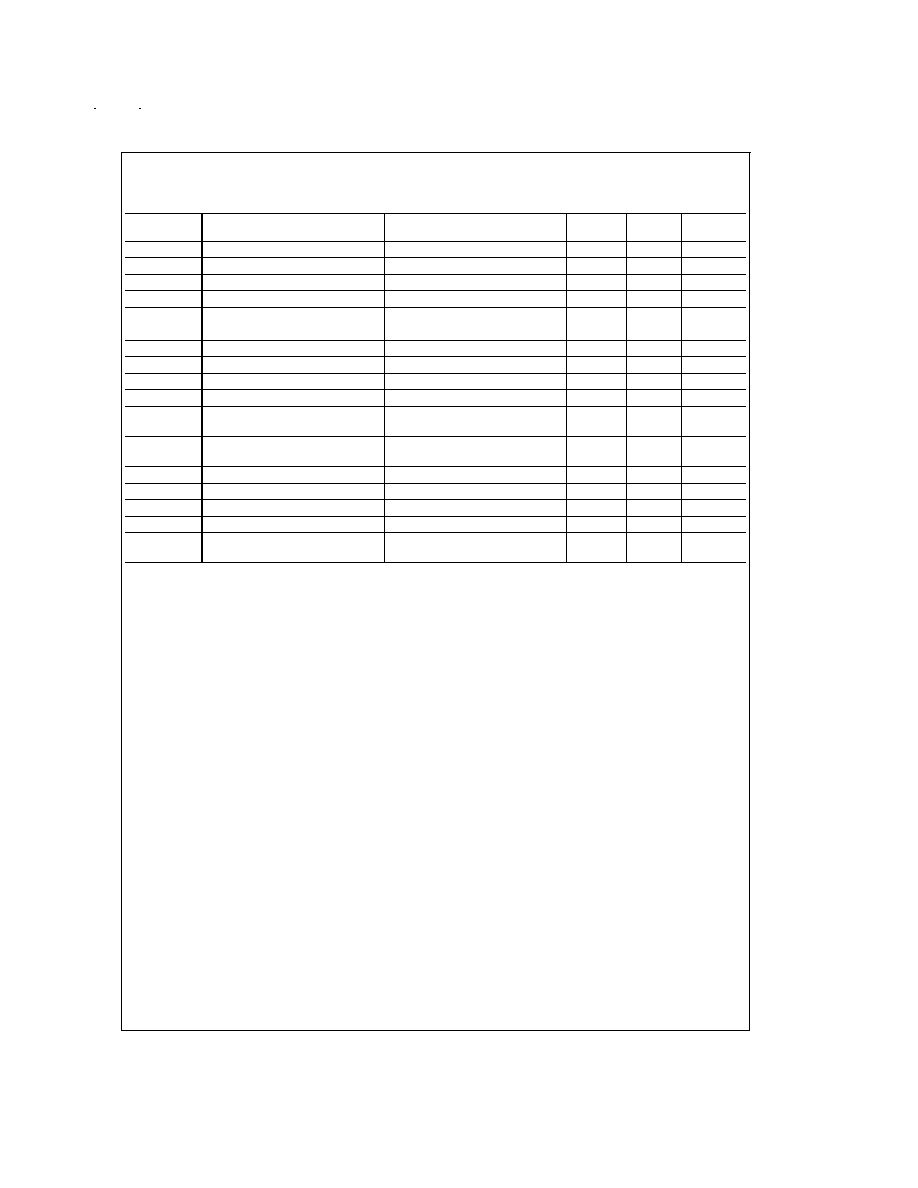
AC Electical Characteristics
(Continued)
T
A
= 25∞C; V
CC1
= V
CC2
= 8V. Manually adjust Video Output pins 13, 15, and 18 to 4V DC for the AC test unless otherwise
stated. (Note 15)
Symbol
Parameter
Conditions
Typical
(Note 5)
Limit
(Note 6)
Units
A
V 0.25V
Contrast Attenuation
@
0V
Ref: A
V
max, V
10
= 0V
-35
dB
Drive
Drive Control Range
V
drive
= 0V to 4V, V
10
= 4V
12
dB
A
V match
Absolute Gain Match
@
A
V
max
V
10
= 4V, V
drive
= 4V (Note 9)
±
0.3
dB
A
V track
Gain Change Between Amplifiers
V
10
= 4V to 2V (Notes 9, 10)
±
0.3
dB
f(-3 dB)
Video Amplifier Bandwidth
V
10
= 4V, V
drive
= 4V,
110
MHz
(Notes 11, 12))
V
O
= 3.5 V
P-P
t
r
(Video)
Video Output Rise Time
V
O
= 3.5 V
P-P
(Note 11)
3.6
ns
t
f
(Video)
Video Output Fall Time
V
O
= 3.5 V
P-P
(Note 11)
3.2
ns
V
sep
10 kHz
Video Amplifier 10 kHz Isolation
V
10
= 4V (Note 13)
-70
dB
V
sep
10 MHz
Video Amplifier 10 MHz Isolation
V
10
= 4V (Notes 11, 13)
-50
dB
V
OL
(OSD)
OSD Black Level, Difference from
Video Black Level
V
OSD in
= 0.8V, OSD Mode
-0.4
-0.7
V (max)
V
OH
(OSD)
OSD Output High Voltage (above
measured video black level)
V
OSD in
= 2.5V, OSD Mode
2.1
2.4
V (max)
t
r
(OSD)
Going into OSD Mode
OSD Mode (
Figure 2)
5.0
ns
t
f
(OSD)
Going out of OSD Mode
OSD Mode (
Figure 2)
10.0
ns
t
r-prop
(OSD)
Starting OSD Propagation Delay
Switching to OSD Mode (
Figure 3)
13.0
ns
t
f-prop
(OSD)
Ending OSD Propagation Delay
Switching to Vid. Mode (
Figure 3)
14.0
ns
T
pw
(Clamp)
Input Clamp Pulse Width (Part of
Sandcastle Sync)
(Note 14)
200
ns (min)
Note 1: Absolute Maximum Ratings indicate limits beyond which damage to the device may occur.
Note 2: Operating Ratings indicate conditions for which the device is functional, but do not guarantee specific performance limits. For guaranteed specifications and
test conditions, see the Electrical Characteristics. The guaranteed specifications apply only for the test conditions listed. Some performance characteristics may de-
grade when the device is not operated under the listed test conditions.
Note 3: V
CC
supply pins 2 and 16 must be externally wired together to prevent internal damage during V
CC
power on/off cycles.
Note 4: Human body model, 100 pF discharged through a 1.5 k
resistor.
Note 5: Typical specifications are specified at +25∞C and represent the most likely parametric norm.
Note 6: Tested limits are guaranteed to National's AOQL (Average Outgoing Quality Level).
Note 7: The supply current specified is the current for V
CC1
and V
CC2
minus the current through R
L
(I
supply
= I
CC1
+ I
CC2
- I
L
). The supply current for V
CC2
(pin 16)
does depend on the output load. With video output at 1V DC, the additional current through V
CC2
is 7.7 mA with R
L
= 390
.
Note 8: Output voltage is dependent on load resistor. Test circuit uses R
L
= 390
.
Note 9: Measure gain difference between any two amplifiers. V
IN
= 635 mV
PP
.
Note 10:
A
V
track is a measure of the ability of any two amplifiers to track each other and quantifies the matching of the three attenuators. It is the difference in
gain change between any two amplifiers with the contrast voltage (V
10
) at either 4V or 2V measured relative to an A
V
max condition, V
10
= 4V. For example, at A
V
max the three amplifiers' gains might be 17.1 dB, 16.9 dB, and 16.8 dB and change to 11.2 dB, 10.9 dB and 10.7 dB respectively for V
10
= 2V. This yields the mea-
sured typical
±
0.1 dB channel tracking.
Note 11: When measuring video amplifier bandwidth or pulse rise and fall times, a double sided full ground plane printed circuit board without socked is recom-
mended. Video amplifier 10 MHz isolation test also requires this printed circuit board. The reason for a double sided full ground plane PCB is that large measurement
variations occur in single sided PCBs.
Note 12: Adjust input frequency from 10 MHz (A
V
max reference level) to the -3 dB corner frequency (f
-3 dB
).
Note 13: Measure output levels of the other two undriven amplifiers relative to the driven amplifier to determine channel separation. Terminate the undriven amplifier
inputs to simulate generator loading. Repeat test at f
IN
= 10 MHz for V
sep
10 MHz.
Note 14: A minimum pulse width of 200 ns is guaranteed for a horizontal line of 15 kHz. This limit is guaranteed by design. If a lower line rate is used then a longer
clamp pulse may be required.
Note 15: During the AC test the 4V DC level is the center voltage of the AC output signal. For example, if the output is 4 V
PP
the signal will swing between 2V DC
and 6V DC.
Note 16: Machine Model ESD test is covered by specification EIAJ IC-121-1981. A 200 pF cap is charged to the specified voltage, then discharged directly into the
IC with no external series resistor (resistance of discharge path must be under 50
).
www.national.com
3
Timing Diagrams
DS100091-2
FIGURE 2. OSD Rise and Fall Times
DS100091-3
FIGURE 3. OSD Propagation Delays
DS100091-4
FIGURE 4. Sandcastle Sync Pulse
www.national.com
4
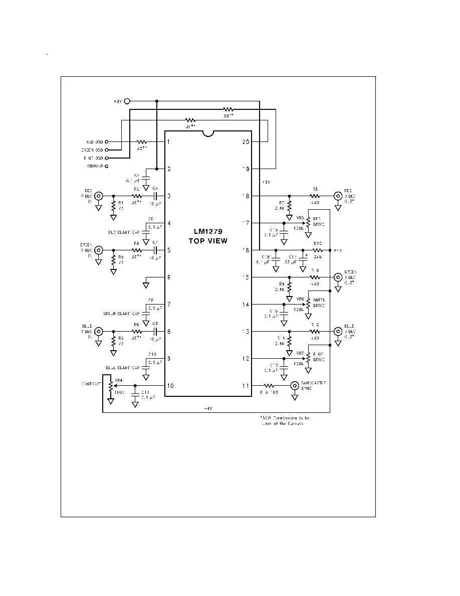
Test Circuits
DS100091-5
**Note: All video inputs
must have a series 30
resistor for protection against EOS (Electrical Over Stress). If the OSD signals are external to the monitor, or
these signals are present any time when +8V is not fully powered up, then the OSD inputs also
require a series 30
resistor.
FIGURE 5. LM1279 OSD Video Pre-amp Demonstration Board Schematic
www.national.com
5
Pin Descriptions
Pin
No.
Pin
Name
Schematic
Description
1
Red OSD Input
These are standard TTL inputs. An OSD
signal at any of the three pins will
automatically switch the pre-amp into the
OSD mode. 7 colors, including white, are
available.
19
Blue OSD Input
20
Green OSD Input
2
V
CC1
Power supply pin (excluding output stage)
3
Red Video In
Video inputs. These inputs
must be AC
Coupled with a minimum of a 1 µF cap, 10
µF is preferred. A series resistor of about
33
must be used for ESD protection.
5
Green Video In
8
Blue Video In
4
Red Clamp Cap
The external clamp cap is charged and
discharged to the correction voltage
needed for DC restoration. 0.1 µF is the
recommended value.
7
Green Clamp Cap
9
Blue Clamp Cap
6
Ground
Ground pin.
10
Contrast
Contrast control pin:
4V - no attenuation
0V - over 40 dB attenuation
Drive control pins:
4V - no attenuation
0V - 20 dB attenuation
12
Blue Drive
14
Green Drive
17
Red Drive
11
Sandcastle Input
The sandcastle input allows for blanking
only, or blanking with DC restoration.
Blanking requires a 2V input. Clamping
with blanking requires a 4V input.
13
Blue Video Out
Video output. For proper black level the
output must drive 390
impedance.
15
Green Video Out
18
Red Video Out
www.national.com
6
Pin Descriptions
(Continued)
Pin
No.
Pin
Name
Schematic
Description
16
V
CC2
Power supply pin for the output stage.
There are no internal connections to V
CC1
.
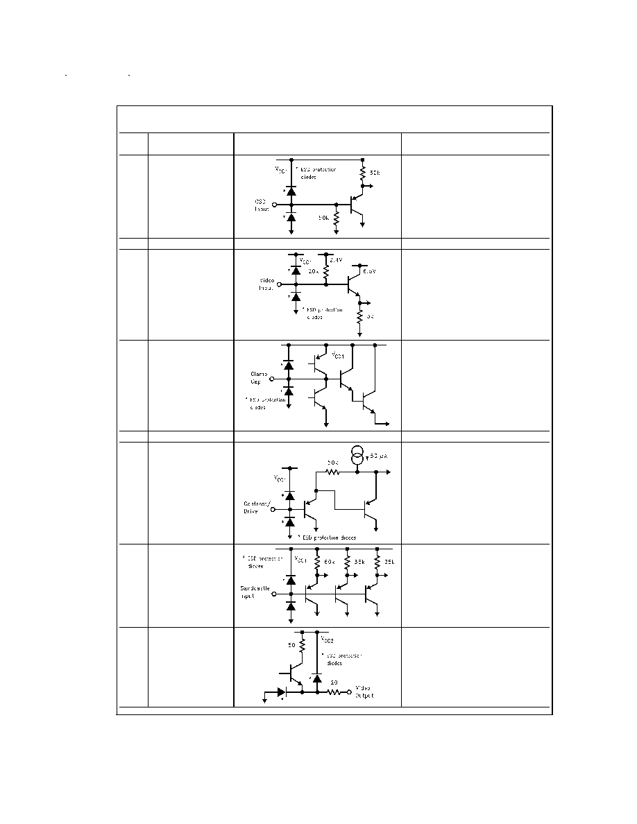
ESD and Arc-Over Protection
The ESD cells of the LM1279 are improved over the ESD
cells used in typical video pre-amps. The monitor designer
must still use good PC board layout techniques when de-
signing with the LM1279. The human body model ESD sus-
ceptibility of these parts is rated at 3 kV (Note 4). However,
many monitor manufacturers are now testing their monitors
to the level 4 of the IEC 801-2 specification. This requires the
inputs to the monitor to survive an 8 kV discharge. If the
monitor designer expects to survive such levels he MUST
provide external ESD protection to the video pre-amp inputs!
PC board layout is very important with LM1279 as with other
video pre-amps. The LM1279 provides excellent protection
against ESD and arc-over, but the LM1279 is not a substitute
for good PCB layout.
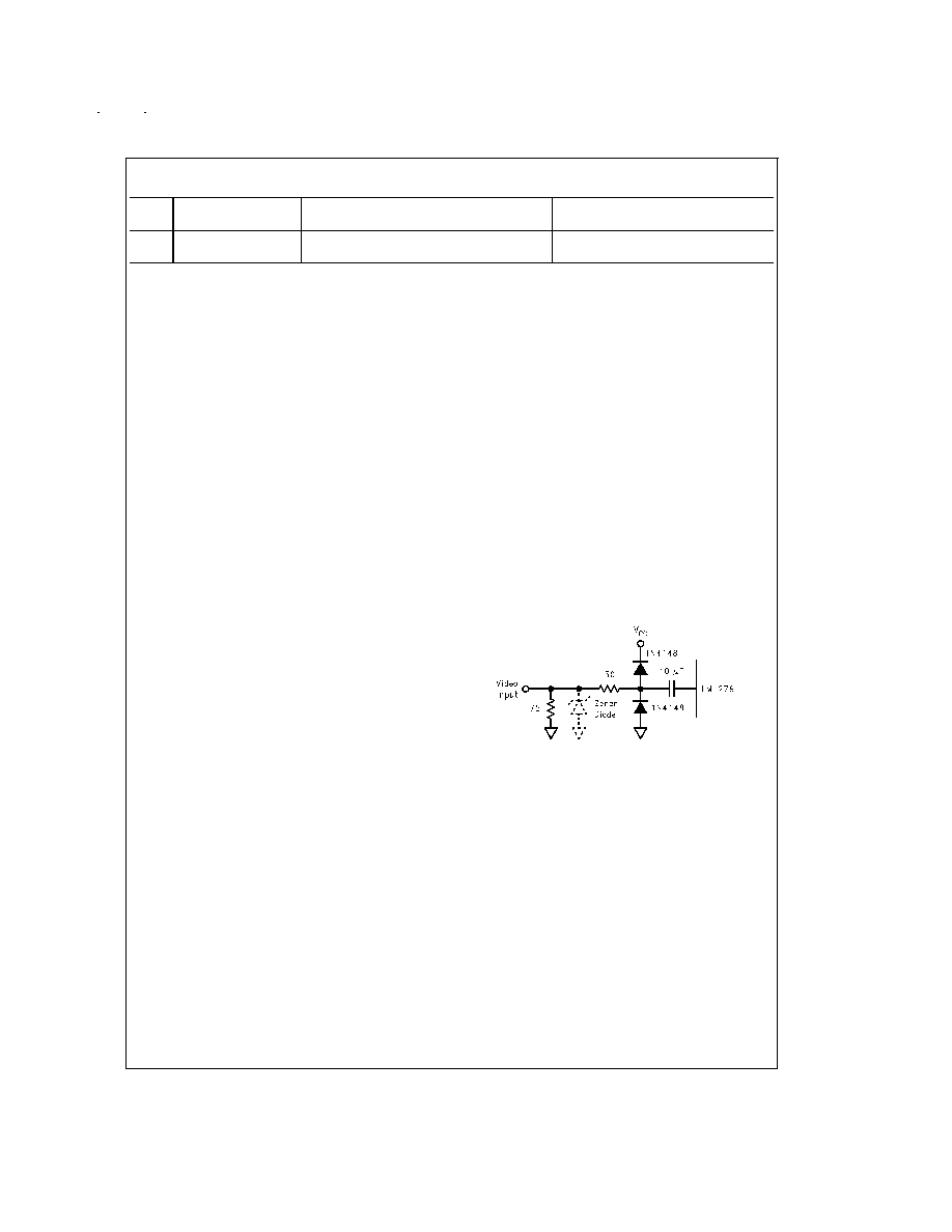
Figure 6 shows the recommended input protection for a
video pre-amp. The two diodes at the video pre-amp input
and after the 30
series resistor offers the best protection
against ESD. When this protection is combined with a good
PCB layout, the video pre-amp will easily survive the IEC
801-2 level 4 (8 kV ESD) testing commonly done by monitor
manufacturers. If the protection diodes are moved to the
video input side of the 30
resistor, then the ESD protection
will be less effective. There is also the risk of damaging the
diodes since there is no resistor for current limiting. In such
a design a heavier duty diode, such as the FDH400, should
be used. It is strongly recommended that the protection di-
odes be added as shown in
Figure 6. The 1N4148 diode has
a maximum capacitance of 4 pF. This would have little affect
on the response of the video system due to the low imped-
ance of the input video.
Many monitor designers prefer to use a single zener diode
instead of the recommended two diodes at the video pre-
amp input. The required location of the zener diode is shown
in
Figure 6. It is shown as a dashed line, indicating an alter-
native to the two diode solution. The zener diode does give
the savings of one component, but now the protection is less
effective. To minimize capacitance, the zener diode needs to
have a zener voltage of 24V or higher. This is well above the
V
CC
voltage of the LM1279. The zener diode must be lo-
cated at the video input for protection against a low voltage
surge. The 30
resistor is needed to limit the current of such
a voltage surge, protecting the video pre-amp. Protection
against ESD by using a zener diode is about as effective as
having the two diodes at the video input (same location as
the zener diode). A higher series resistor may be necessary
for protection against the zener voltage, but the higher resis-
tor value will impair the performance of the LM1279; result-
ing in a lower bandwidth and a less stable black level. For
maximum reliability the monitor designer should not consider
the zener diode solution for ESD protection of the LM1279.
The ESD cells of the LM1279 also gives good tolerance
against arc-over. Once again the monitor designer must be
careful in his PCB layout for good arc-over protection. In the
video chain only the outputs of the CRT driver are directly
exposed to the voltages that may occur during arc-over. A
good PCB layout is the best protection for the video pre-amp
against arc-over. The pre-amp vulnerability is mainly through
the ground traces on the PCB. For proper operation all
ground connections associated with the video pre-amp, in-
cluding the grounds to the bypass capacitors, must have
short returns to the ground pins. A significant ground plane
should be used to connect all the pre-amp grounds.
Figure
16, the demo board layout, is an excellent example on an ef-
fective ground plane, yet using only a single sided PCB lay-
out. Here is a check list to make sure a PC board layout has
good grounding:
∑
All associated grounds with the video pre-amp are con-
nected together through a large ground plane.
∑
CRT driver ground is connected to the video pre-amp
ground at one point.
∑
CRT and arc protection grounds are connected directly to
chassis, or the main ground. There is no arc-over current
flow from these grounds through the pre-amp or CRT
driver grounds.
If any one of the above suggestions are not followed, then
the LM1279 may become vulnerable to arc-over. Improper
grounding is by far the most common cause of a video pre-
amp failure during arc-over.
Functional Description
Figure 1 on the front page shows the block diagram of the
LM1279 along with the pinout of the IC. Each channel re-
ceives a video input signal at its input amplifier (-A1). The
output of the input amplifier goes to the contrast attenuator
stage. For easy interfacing to 5V DACs all controls inputs, in-
cluding the contrast control, use a 0V to 4V range. The con-
trast control has no attenuation with an input of 4V, and has
full attenuation (over -40 dB) with a 0V input. All three chan-
nels will accurately track the contrast control setting at pin
10. Each channel will have the same amount of attenuation
for a given input voltage typically to within
±
0.3 dB. All chan-
nels will track because the contrast control is the first stage
of attenuation and the internal control voltage generated
from the input voltage is common to all three channels.
The output of the contrast attenuator goes to the drive at-
tenuator. This stage has a 12 dB control range. This stage is
used for color balance, so the adjustment range has been
limited to 12 dB for a more accurate color balance. Each
DS100091-12
FIGURE 6. Recommended Video Input ESD Protection
www.national.com
7

Functional Description
(Continued)
channel has its own independent control pin with the 0V to
4V control range. An input of 4V give no attenuation, and an
input of 0V gives the full 12 dB attenuation.
The output of the drive attenuator stage goes to the inverting
input of A2. Since this is the second inversion stage, the out-
put of A2 will be the non-inverted video signal. Note that the
output of gm1 goes to the non-inverting input of A2. Also note
that the output of A2 goes to the inverting input of gm1. This
is the feedback for the clamp circuitry. The output stage of A2
is an exact duplicate of the video output through A3. If a
390
load impedance is used at the video output, then the
black level at the output stage will accurately track the output
of A2. The other input to gm1 is the desired black level output
of the LM1279. Since the LM1279 has a fixed black level out-
put, the non-inverting inputs to gm1 in all three channels go
to a fixed 1.35V internal reference. This sets the black level
output to a nominal 1.35V. gm1 acts like a sample and hold
amplifier. Once the sandcastle sync exceeds 3.6V gm1 is ac-
tivated, driving the input of A2 to a level where the video out-
put will be 1.35V. For proper DC restoration it is important
that gm1 be activated only during the horizontal flyback time
when the video is at the black level. gm1 also charges the
clamp cap to the correct voltage to maintain a 1.35V black
level at the video output. When gm1 is turned off the voltage
stored on the clamp cap will maintain the correct black level
during the active video, thus restoring the DC level for a
1.35V black level.
The input of A3 receives the output from A2. The video chan-
nel of A3 is a duplication of the output stage to A2. As men-
tioned in the previous paragraph this is done so that the DC
restoration can be done at the A2 stage. A3 also receives the
OSD input and a sandcastle input for blanking. By doing DC
restoration at the A2 stage, OSD or blanking can be acti-
vated at the output stage during the time DC restoration is
being done at A2. There is an interface circuit between the
sandcastle input and the A3 output stages. This interface cir-
cuit will activate the blanking if the sandcastle sync input is
between 1.7V and 6.0V. The blanking mode will force the
output down to a level of about 0.1V. This is a blacker-than-
black level and can be used for blanking at the cathodes of
the CRT.
Once the sandcastle exceeds 6.5V, then the output will no
longer be in the blanked mode, but DC restoration is still be-
ing done on the video signal.
The OSD signal goes into a special interface circuit. The out-
put of this circuit will drive the output of A3 to either an OSD
black level or to about 2.4V above the video black level
(OSD white level). The OSD black level is about 300 mV be-
low the video black level. This guarantees that if the OSD
signal is not activated for a particular channel, then its output
will be slightly below the cutoff level. If an OSD input is re-
ceived in a particular channel, then the video output will be at
the OSD white level. The OSD mode is automatically acti-
vated if there is only one OSD signal to any of the video
channels. This OSD control circuit will allow any color, ex-
cept black, during the OSD mode. This also saves the need
for a special signal to switch into the OSD mode. Remember
that at least one OSD input must be high to enable the OSD
mode, therefore black can't be used in the OSD window.
Sandcastle Sync
This special sync signal is used to allow for a 20-pin OSD
video pre-amp with all the desired controls. By using a sand-
castle sync, both clamping and blanking can be activated
from the same pin. Figure 4 shows the sandcastle sync sig-
nal. There are four possible modes of operation with the
Sandcastle pulse. These modes are:
1.
Inactive Region
2.
Blanking and no Clamping
3.
Blanking and Clamping
4.
Clamping and no Blanking
Figure 4 also shows the voltage levels where the LM1279
switches from one mode to the other mode. As an example
the LM1279 will switch from the inactive mode to the blank-
ing and no clamping mode between 1.2V and 1.7V. For
proper operation the inactive input must be safely below the
1.2V level. The blanking with no clamping pulse must be
safely above 1.7V and below 2.8V. Blanking and clamping
must be between 3.6V and 5.8V. Clamping and no blanking
must be above 6.5V with the maximum voltage being limited
by V
CC
.
If the monitor designer desires to blank at the cathode, then
he would go into the blanking and no clamping mode for
most of the flyback period. During this period it is also neces-
sary to do DC restoration. During this time the LM1279
should be operated in the blanking and clamping mode. In
this mode DC restoration is done without interfering with
blanking.
In some designs the horizontal phase shift capability of the
monitor is very large. In these designs the video can be
moved so the flyback period can be displayed during the ac-
tive trace period for the video. Now the clamping could be
done during the normal video sweep time. During this period
clamping with blanking will give a black bar on the CRT
screen. This is not a normal operating mode of the monitor,
but the monitor designer still may prefer not to display this
black bar. Under this condition the clamp pulse must be
above 6.5V.
A simple two transistor sandcastle generator is covered in
separate application note. This circuit will generate all four
states for the sandcastle sync, including the clamp with no
blanking when the clamping function occurs during the pe-
riod for active video. The switching time between the inactive
region and the clamp only region must be less than 30 ns if
complete elimination of any blanking pulse is required in an
application.
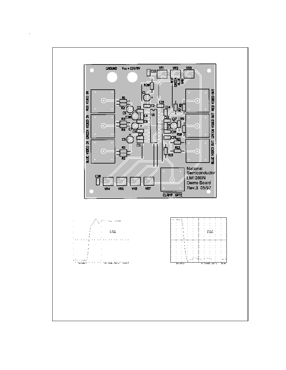
Applications of the LM1279
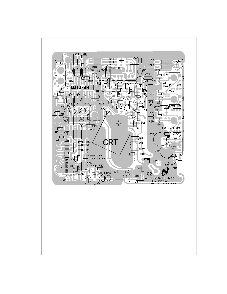
Two demonstration boards are available to evaluate the
LM1279. One board is the pre-amp demonstration board.
This board was used for testing and characterizing the
LM1279. The schematic for this board is shown in
Figure 5
and the printed circuit layout for this board is shown in
Figure
7. The other board is a complete video channel neck board
that can be directly plugged into the CRT socket. The sche-
matic for this board is shown in
Figure 10 and the printed cir-
cuit layout is shown in
Figure 11. The CRT driver used on
this board is the LM2407. Any of National's monolithic CRT
drivers can be used in this board, but the LM2407 is consid-
ered the best match to the LM1279 based on cost and per-
formance.
Some important notes on
Figure 5. All three video inputs
have a 75
terminating resistor for a 75
video system. This
is the normal video impedance of the video from a computer
system. It is possible to also have a 50
system, then R1,
R3, and R5 would be changed to 50
. R2, R4, and R6 are in
series with the video inputs of the LM1279. These three 30
resistors are required to protect the IC from any sudden volt-
www.national.com
8

Applications of the LM1279
(Continued)
age surges that may result during the power up and power
down modes, or when connecting the monitor to other equip-
ment. The monitor designer must include these resistors in
his design for good monitor reliability. If additional protection
against ESD at the video inputs is necessary, then adding
clamp diodes on the IC side of the 30
resistors is recom-
mended, one to V
CC1
and one to ground (see
Figure 6).
Sometimes a designer may want to increase the value of the
30
resistors at the video inputs, for additional ESD protec-
tion. This is not recommended with the LM1279. C5, C7, and
C9 are part of the DC restoration circuit. This circuit is de-
pending on a total maximum circuit resistance of about
110
; 30
input series resistor plus 75
for the video termi-
nation resistor. Increasing the value of the 30
resistors will
exceed the 110
limit. The excellent internal ESD protection
and the external clamp diodes (if needed) will provide excel-
lent ESD protection.
The 30
resistors in series with the OSD inputs are also
necessary if the OSD signals are external to the monitor, or
if these signals are present any time when the +8V is not
fully powered up. Interfacing to the OSD inputs is quite easy
since the signal processing necessary to match the OSD sig-
nals to the video levels is done internal by the LM1279.
There is also no need for an OSD window signal. Any time
there is a high TTL signal at any of the three OSD inputs, the
LM1279 will automatically switch to the OSD mode. A high
TTL OSD signal will give a high video output for that color.
The OSD level is fixed, typically 2.3V above the video black
level. This will give a fixed brightness to the OSD window,
but not at maximum video brightness which could be un-
pleasant to the user.
Figure 2 and Figure 3 show the timing
diagrams of the OSD signals for the LM1279.
The recommended load impedance for the LM1279 is 390
.
However, some changes in the load impedance can be
made. If the load impedance is reduced, the monitor de-
signer must confirm that the part is still operating in its proper
die temperature range, never exceeding a die temperature
of 150∞C. When changing the load impedance, the black
level shift is shown in the chart below. The measured V
P-P
output with under 1% distortion is also listed.
Load
V
P-P
Blk. Level Shift
430
3.62V
+15 mV
390
3.62V
0 mV
330
3.58V
-25 mV
270
3.51V
-45 mV
When using a lower load impedance, the LM1279 does go
into hard clipping more quickly. This does reduce the head-
room of the video output.
Board layout is always critical in a high frequency application
such as using the LM1279. A poor layout can result in ringing
of the video waveform after sudden transitions, or the part
could actually oscillate. A good ground plane and proper
routing of the +8V are important steps to a good PCB layout.
The LM1279 does require very good coupling between V
CC1
and V
CC2
(pins 2 and 16). This is clearly shown in
Figure 7
and
Figure 11 with the short and large trace between pins 2
and 16. Both demonstration boards offer the monitor de-
signer an excellent example of good ground plane being
used with the LM1279. These boards are single sided, yet al-
low the LM1279 to operate at its peak performance. The
neck board also shows a good example of interfacing to a
CRT driver and to the CRT. The video signal path is kept as
short as possible between the LM1279 and the CRT driver,
and also between the CRT driver and the CRT socket. Actual
performance of the LM1279 in the video pre-amp demon-
stration board is shown in
Figure 8 and Figure 9.
References
Ott, Henry W.
Noise Reduction Techniques in Electronic
Systems, John Wiley & Sons, New York, 1976
Zahid Rahim, "Guide to CRT Video Design," Application
Note 861, National Semiconductor Corp., Jan. 1993
www.national.com
9
Applications of the LM1279
DS100091-13
FIGURE 7. LM1279 OSD Video Pre-≈mp Demontration Board Layout
DS100091-16
FIGURE 8. LM1279 Rise Time
DS100091-17
FIGURE 9. LM1279 Fall Time
www.national.com
10

Applications of the LM1279
(Continued)
DS100091-14
FIGURE
10.
LM1279/LM2407
Demonstration
Neck
Board
Schematic
www.national.com
11
Applications of the LM1279
(Continued)
DS100091-15
FIGURE 11. LM1279/LM2407 Demonstration Neck Board Layout
www.national.com
12

13
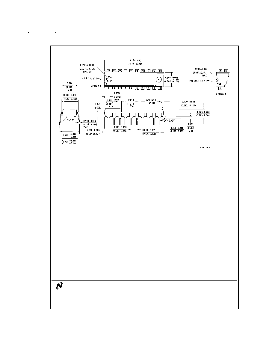
Physical Dimensions
inches (millimeters) unless otherwise noted
LIFE SUPPORT POLICY
NATIONAL'S PRODUCTS ARE NOT AUTHORIZED FOR USE AS CRITICAL COMPONENTS IN LIFE SUPPORT DE-
VICES OR SYSTEMS WITHOUT THE EXPRESS WRITTEN APPROVAL OF THE PRESIDENT OF NATIONAL SEMI-
CONDUCTOR CORPORATION. As used herein:
1. Life support devices or systems are devices or sys-
tems which, (a) are intended for surgical implant into
the body, or (b) support or sustain life, and whose fail-
ure to perform when properly used in accordance
with instructions for use provided in the labeling, can
be reasonably expected to result in a significant injury
to the user.
2. A critical component in any component of a life support
device or system whose failure to perform can be rea-
sonably expected to cause the failure of the life support
device or system, or to affect its safety or effectiveness.
National Semiconductor
Corporation
Americas
Tel: 1-800-272-9959
Fax: 1-800-737-7018
Email: support@nsc.com
www.national.com
National Semiconductor
Europe
Fax: +49 (0) 1 80-530 85 86
Email: europe.support@nsc.com
Deutsch Tel: +49 (0) 1 80-530 85 85
English
Tel: +49 (0) 1 80-532 78 32
FranÁais Tel: +49 (0) 1 80-532 93 58
Italiano
Tel: +49 (0) 1 80-534 16 80
National Semiconductor
Asia Pacific Customer
Response Group
Tel: 65-2544466
Fax: 65-2504466
Email: sea.support@nsc.com
National Semiconductor
Japan Ltd.
Tel: 81-3-5620-6175
Fax: 81-3-5620-6179
Order Number LM1279N
NS Package Number N20A
LM1279
1
1
0
MHz
RGB
V
ideo
Amplifier
System
with
OSD
National does not assume any responsibility for use of any circuitry described, no circuit patent licenses are implied and National reserves the right at any time without notice to change said circuitry and specifications.