 | –≠–ª–µ–∫—Ç—Ä–æ–Ω–Ω—ã–π –∫–æ–º–ø–æ–Ω–µ–Ω—Ç: LM1282N | –°–∫–∞—á–∞—Ç—å:  PDF PDF  ZIP ZIP |
LM1282
110 MHz RGB Video Amplifier System with On Screen
Display (OSD)
General Description
The LM1282 is a full feature video amplifier with OSD inputs,
all within a 28-pin package. This part is intended for use in
monitors with resolutions up to 1280 x 1024. The video sec-
tion of the LM1282 features three matched video amplifiers
with blanking. All of the video amplifier adjustments feature
high input impedance 0V to 4V DC controls, providing easy
interfacing to bus controlled alignment systems. The OSD
section features three TTL inputs and a DC contrast control.
The switching between the OSD and video section is con-
trolled by a single TTL input. Although the OSD signals are
TTL inputs, these signals are internally processed to match
the OSD logic low level to the video black level. When ad-
justing the drive controls for color balance of the video sig-
nal, the color balance of the OSD display will track these
color adjustments. The LM1282 also features an internal
spot killer circuit to protect the CRT when the monitor is
turned off. For applications without OSD insertion please re-
fer to the LM1205 or LM1208 data sheets.
Features
n
Three wideband video amplifiers 110 MHz
@
-3 dB
(4 V
PP
output)
n
TTL OSD inputs, 50 MHz bandwidth
n
On chip blanking, outputs under 0.1 V when blanked
n
High speed Video/OSD switch
n
Independent drive control for each channel for color
balance
n
0V to 4V, high impedance DC contrast control with over
40 dB range
n
0V to 4V, high impedance DC drive control (0 dB to
-12 dB range)
n
0V to 4V, high impedance DC OSD contrast control with
over 40 dB range
n
Capable of 7 V
PP
output swing (slight reduction in
bandwidth)
n
Output stage directly drives most hybrid or discrete CRT
drivers
Applications
n
High resolution RGB CRT monitors requiring OSD
capability
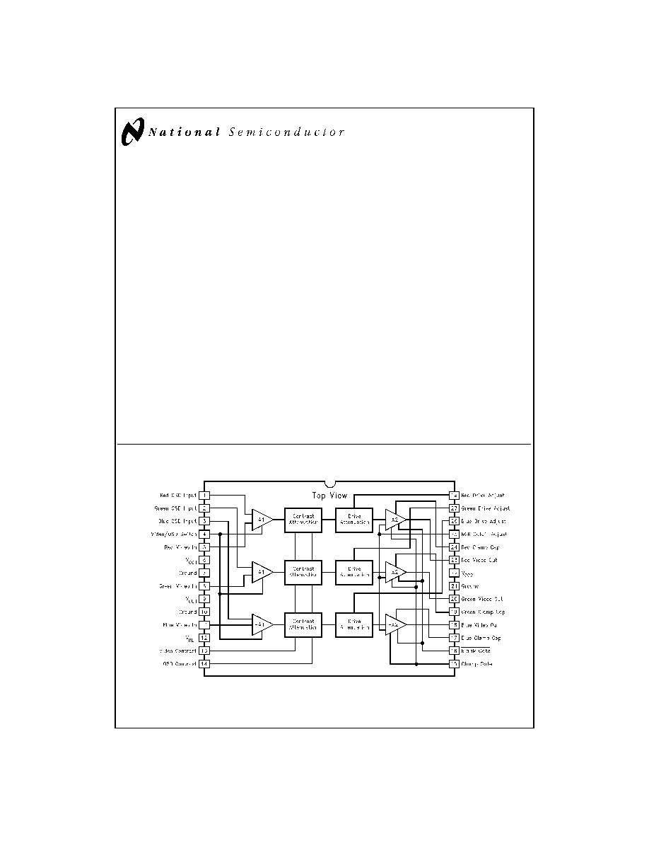
Block and Connection Diagram
DS012519-1
FIGURE 1. Order Number LM1282N
See NS Package Number N28B
June 1998
LM1282
1
10MHz
RGB
V
ideo
Amplifier
System
with
On
Screen
Display
(OSD)
© 1998 National Semiconductor Corporation
DS012519
www.national.com
Absolute Maximum Ratings
(Note 1)
If Military/Aerospace specified devices are required,
please contact the National Semiconductor Sales Office/
Distributors for availability and specifications.
Supply Voltage
Pins 6, 9, and 22
15V
Peak Video Output Source Current
(Any One Amp) Pins 18, 20, and 23
28 mA
Voltage at Any Input Pin (V
IN
)
V
CC
V
IN
GND
Power Dissipation (P
D
)
(Above 25∞C Derate based on
JA
and T
J
)
2.5W
Thermal Resistance to Ambient (
JA
)
45∞C/W
Thermal Resistance to Case (
JC
)
28∞C/W
Junction Temperature (T
J
)
150∞C
ESD Susceptibility (Note 4)
2 kV
ESD Machine Model (Note 17)
200V
Storage Temperature
-65∞C to 150∞C
Lead Temperature
(Soldering, 10 sec.)
265∞C
Operating Ratings
(Note 2)
Temperature Range
-20∞C to 70∞C
Supply Voltage (V
CC
)
11.4V
V
CC
12.6V
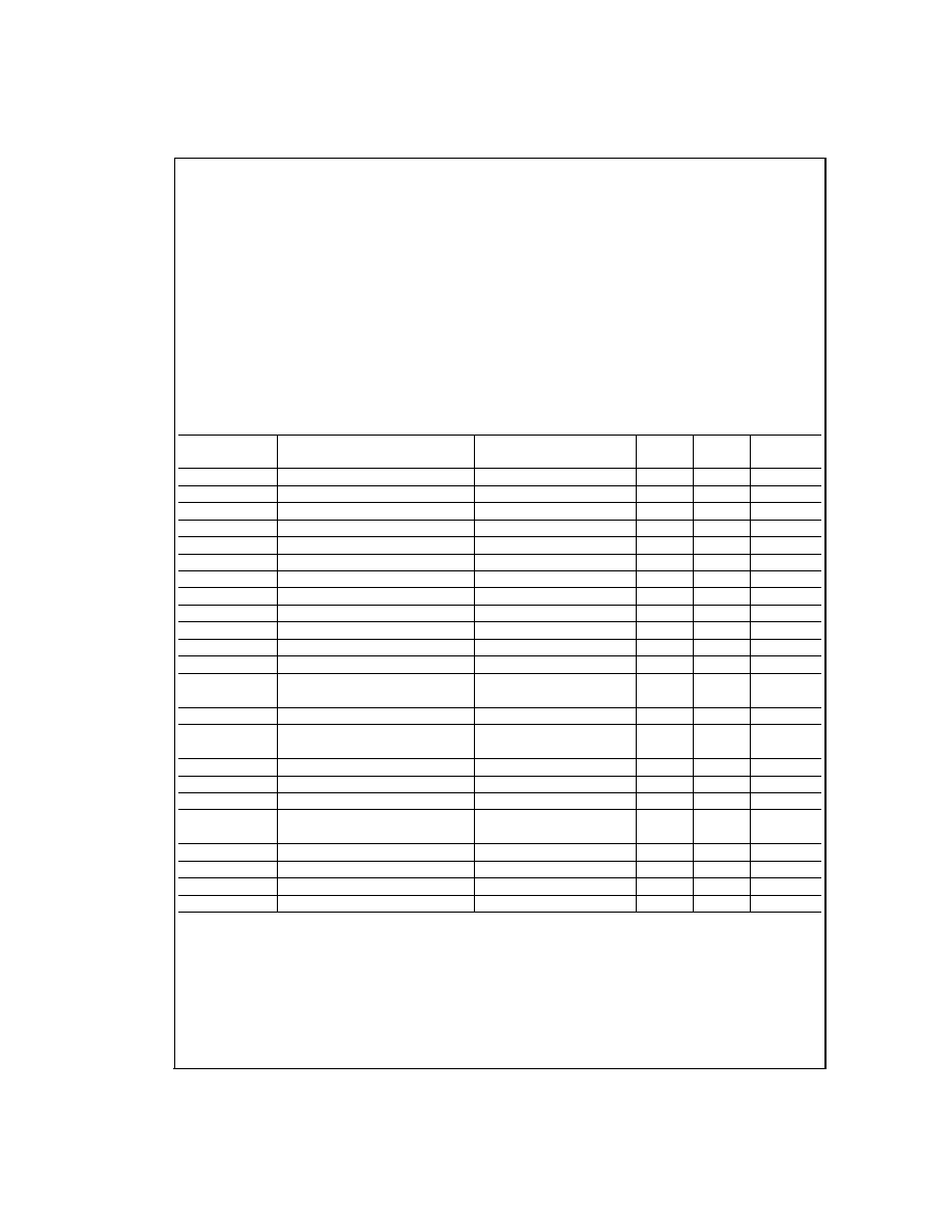
DC Electrical Characteristics
See DC Test Circuit (
Figure 2), T
A
= 25∞C; V
CC1
= V
CC2
= 12V; V
13
= 4V; V
14
= 4V; V
16
= 4V; V
drive
= 4V; V
4
= 0V; V
15
=
0V; V
25
= 1V unless otherwise stated
Symbol
Parameter
Conditions
Typical
Limit
Units
(Note 5)
(Note 6)
I
S
Supply Current
V
CC1
+ V
CC2
, R
L
=
(Note 7)
95
120
mA (max)
R
IN
Video Input Resistance
Any One Amplifier
100
k
V
15l
Clamp Gate Low Input Voltage
Clamp Comparators On
1.2
0.8
V (max)
V
15h
Clamp Gate High Input Voltage
Clamp Comparators Off
1.6
2.0
V (min)
I
15l
Clamp Gate Low Input Current
V
15
= 0V
-2.5
µA (max)
I
15h
Clamp Gate High Input Current
V
15
= 12V
0.01
1.0
µA (max)
V
16l
Blank Gate Low Input Voltage
Blank Gate On
1.2
0.8
V (max)
V
16h
Blank Gate High Input Voltage
Blank Gate Off
1.6
2.0
V (min)
I
16l
Blank Gate Low Input Current
V
16
= 0V
-1.5
µA (max)
I
16h
Blank Gate High Input Current
V
16
= 12V
0.01
1.0
µA (max)
V
12
Reference Voltage
2.0
V
I
vid-clamp
Video Input Cap Charge Current
Clamp Comparators On
±
900
±
450
µA (min)
I
vid-bias
Video Input Cap Bias Discharge
Clamp Comparators Off
±
450
nA
Current
I
out-clamp
Output Clamp Cap Charge Current
Clamp Comparators On
±
850
±
450
µA (min)
I
out-bias
Output Clamp Cap Bias Discharge
Clamp Comparators Off
450
nA
Current
V
OL
Video Output Low Voltage
V
25
= 0V
50
100
mV (max)
V
OH
Video Output High Voltage
V
25
= 10V
8.0
7.5
V (min)
V
O(1V)
Video Black Level Output Voltage
V
25
= 1V
1.1
V (Note 8)
V
O(1V)
Video
Black Level Output Voltage
Between Any Two Amplifiers,
±
20
±
250
mV (max)
V
25
= 1V
V
OL
(blanked)
Video Output Blanked Voltage
Blank Gate On (V
16
0.8V)
100
500
mV (max)
I
13,14, 26, 27, or 28
Contrast/Drive Control Input Current
V
contrast
= V
drive
= 0V to 4V
-125
-500
nA (max)
I
25
Cut-Off Control Input Current
V
25
= 0V to 4V
-0.25
-1.5
µA (max)
V
spot
Spot Killer Voltage
V
CC
Adjusted to Activate
10.6
11.2
V
www.national.com
2
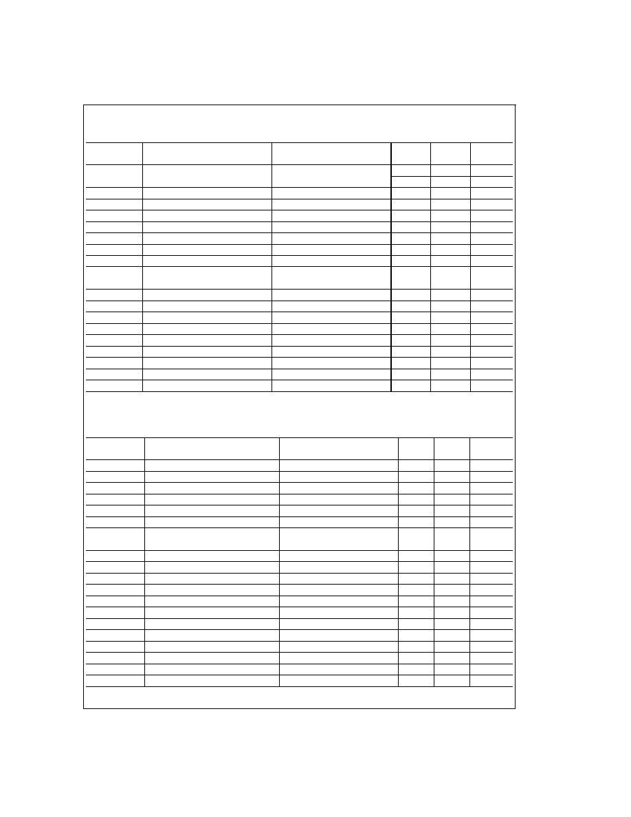
AC Electrical Characteristics
(Note 15)
See AC Test Circuit (
Figure 3) , T
A
= 25∞C, V
CC1
= V
CC2
= 12V; V
4
= 0V. Manually adjust Video Output pins 18, 20, and 23 to
4V DC for the AC test unless otherwise stated
Symbol
Parameter
Conditions
Typical
Limit
Units
(Note 5)
(Note 6)
A
V max
Video Amplifier Gain
V
13
= 4V, V
IN
= 400 mV
PP
10.0
7.0
V/V (min)
V
drive
= 4V
20.0
16.9
dB (min)
A
V 2V
Contrast Attenuation
@
2V
Ref: A
V
max, V
13
= 2V
-6
dB
A
V 0.25V
Contrast Attenuation
@
0.25V
Ref: A
V
max, V
13
= 0.25V
-24
dB
Drive
2V
Drive Attenuation
@
2V
Ref: A
V
max, V
drive
= 2V
-4.5
dB
Drive
0.25V
Drive Attenuation
@
0.25V
Ref: A
V
max, V
drive
= 0.25V
-11
dB
A
V match
Absolute Gain Match
@
A
V
max
V
13
= 4V, V
drive
= 4V (Note 9)
±
0.3
dB
A
V track
Gain Change between Amplifiers
V
13
= 4V to 2V (Notes 9, 10)
±
0.2
dB
THD
Video Amplifier Distortion
V
O
= 1 V
PP
, f = 10 kHz
1
%
f(-3 dB)
Video Amplifier Bandwidth
V
13
= 4V, V
drive
= 3V,
110
MHz
(Notes 11, 12)
V
O
= 4 V
PP
t
r
(Video)
Video Output Rise Time (Note 11)
V
O
= 4 V
PP
3.0
ns
t
f
(Video)
Video Output Fall Time (Note 11)
V
O
= 4 V
PP
4.0
ns
V
sep
10 kHz
Video Amplifier 10 kHz Isolation
V
13
= 4V (Note 13)
-70
dB
V
sep
10 MHz
Video Amplifier 10 MHz Isolation
V
13
= 4V (Notes 11, 13)
-50
dB
t
r
(Blank)
Blank Output Rise Time (Note 11)
Blank Output = 1 V
PP
8
ns
t
f
(Blank)
Blank Output Fall Time (Note 11)
Blank Output = 1 V
PP
14
ns
t
r-prop
(Blank)
End of Blanking Propagation Delay
Blank Output = 1 V
PP
23
ns
t
f-prop
(Blank)
Start of Blanking Propagation Delay
Blank Output = 1 V
PP
20
ns
T
pw
(Clamp)
Back Porch Clamp Pulse Width
(Note 14)
200
ns (min)
OSD Electrical Characteristics
See DC Test Circuit (
Figure 2), T
A
= 25∞C; V
CC1
= V
CC2
= 12V; V
13
= 4V; V
14
= 4V; V
16
= 4V; V
Drive
= 4V; V
4
= 4V; V
15
=
0V; V
25
= 1V unless otherwise stated
Symbol
Parameter
Conditions
Typical
Limit
Units
(Note 5)
(Note 6)
V
OSDI
OSD Input Low Input Voltage
1.2
0.4
V (max)
V
OSDh
OSD Input High Input Voltage
1.6
2.0
V (min)
V
4l
OSD Select Low Input Voltage
Video Inputs are Selected
1.2
0.8
V (max)
V
4h
OSD Select High Input Voltage
OSD Inputs are Selected
1.6
2.0
V (min)
I
4l
OSD Select Low Input Current
V
4
= 0V
-3.0
-6.0
µA (max)
I
4h
OSD Select High Input Current
V
4
= 12V
0.01
1.0
µA (min)
V
O-OSD(1V)
OSD
Black Level Output Voltage,
V
25
= 1V
±
45
±
175
mV (max)
Difference from Video Output
V
OSD-out
OSD Output Voltage V
PP
V
14
= 4V, V
Drive
= 2V
5.0
V
PP
V
OSD-out
OSD Output V
PP
Attenuation
V
14
= 2V, V
Drive
= 2V
50
30
% (min)
V
OSD-out match
Output Match between Channels
V
14
= 4V, V
Drive
= 2V
±
2.0
%
V
OSD-out track
Output Variation between Channels
V
14
= 4V to 2V, V
Drive
= 2V
±
3.5
%
t
r
(OSD S)
Video to OSD Switch Time (Note 11)
V
1
= V
2
= V
3
= 4V (Note 16)
4
ns
t
f
(OSD S)
OSD to Video Switch Time (Note 11)
V
1
= V
2
= V
3
= 4V (Note 16)
11
ns
t
r-prop
(OSD S)
Video to OSD Propagation Delay
V
1
= V
2
= V
3
= V
13
= V
14
= 4V
11
ns
t
f-prop
(OSD S)
OSD to Video Propagation Delay
V
1
= V
2
= V
3
= V
13
= V
14
= 4V
12
ns
t
r
(OSD)
OSD Rise Time at V
O
(Note 11)
V
14
= 4V; V
25
= 1V
4
ns
t
f
(OSD)
OSD Fall Time at V
O
(Note 11)
V
14
= 4V; V
25
= 1V
10
ns
t
r-prop
(OSD)
Starting OSD Propagation Delay
V
14
= 4V; V
25
= 1V
6.5
ns
t
f-prop
(OSD)
Ending OSD Propagation Delay
V
14
= 4V; V
25
= 1V
9
ns
3
www.national.com

OSD Electrical Characteristics
(Continued)
See DC Test Circuit (
Figure 2), T
A
= 25∞C; V
CC1
= V
CC2
= 12V; V
13
= 4V; V
14
= 4V; V
16
= 4V; V
Drive
= 4V; V
4
= 4V; V
15
=
0V; V
25
= 1V unless otherwise stated
Symbol
Parameter
Conditions
Typical
Limit
Units
(Note 5)
(Note 6)
V
feed
10 kHz
Video Feedthrough into OSD
V
14
= 4V; V
25
= 1V;
-70
dB
V
1
= V
2
= V
3
= 0V
V
feed
10 MHz
Video Feedthrough into OSD
V
14
= 4V; V
25
= 1V;
-60
dB
V
1
= V
2
= V
3
= 0V
Note 1: Absolute Maximum Rating indicate limits beyond which damage to the device may occur.
Note 2: Operating Ratings indicate conditions for which the device is functional, but do not guarantee specific performance limits. For guaranteed specifications and
test conditions, see the Electrical Characteristics. The guaranteed specifications apply only for the test conditions listed. Some performance characteristics may de-
grade when the device is not operated under the listed test conditons.
Note 3: V
CC
supply pins 6, 9, and 22 must be externally wired together to prevent internal damage during V
CC
power on/off cycles.
Note 4: Human body model, 100 pF discharged through a 1.5 k
resistor.
Note 5: Typical specifications are specified at +25∞C and represent the most likely parametric norm.
Note 6: Tested limits are guaranteed to National's AOQL (Average Outgoing Quality Level).
Note 7: The supply current specified is the quiescent current for V
CC1
and V
CC2
with R
L
=
, see
Figure 5 's test circuit. The supply current for V
CC2
(pin 22) also
depends on the output load. With video output at 1V DC, the additional current through V
CC2
is 8 mA for
Figure 5 's test circuit.
Note 8: Output voltage is dependent on load resistor. Test circuit uses R
L
= 390
.
Note 9: Measure gain difference between any two amplifiers. V
IN
= 400 mV
PP
.
Note 10:
A
V
track is a measure of the ability of any two amplifiers to track each other and quantifies the matching of the three attenuators. It is the difference in
gain change between any two amplifiers with the contrast voltage (V
13
) at either 4V or 2V measured relative to an A
V
max condition, V
13
= 4V. For example, at A
V
max the three amplifiers' gains might be 17.1 dB, 16.9 dB, and 16.8 dB and change to 11.2 dB, 10.9 dB and 10.7 dB respectively for V
13
= 2V. This yields the mea-
sured typical
±
0.1 dB channel tracking.
Note 11: When measuring video amplifier bandwidth or pulse rise and fall times, a double sided full ground plane printed circuit board without socket is recom-
mended. Video amplifier 10 MHz isolation test also requires this printed circuit board. The reason for a double sided full ground plane PCB is that large measurement
variations occur in single sided PCBs.
Note 12: Adjust input frequency from 10 MHz (A
V
max reference level) to the -3 dB corner frequency (f
-3 dB
).
Note 13: Measure output levels of the other two undriven amplifiers relative to the driven amplifier to determine channel separation. Terminate the undriven amplifier
inputs to simulate generator loading. Repeat test at f
IN
= 10 MHz for V
sep 10 MHz
.
Note 14: A minimum pulse width of 200 ns is guaranteed for a horizontal line of 15 kHz. This limit is guaranteed by design. If a lower line rate is used a longer clamp
pulse may be required.
Note 15: During the AC test the 4V DC level is the center voltage of the AC output signal. For example, if the output is 4 V
PP
the signal will swing between 2V DC
and 6V DC.
Note 16: When V
1
= V
2
= V
3
= 0V and the video input is 0.7V, then t
r
(OSD) = 11 ns and t
f
(OSD) = 4 ns. The Video Output waveform will be inverted from the one
shown in
Figure 3. Thus t
r
(OSD) is actually a fall time and t
f
(OSD) is actually a rise time in this condition.
Note 17: Machine Model ESD test is covered by specification EIAJ IC-121-1981. A 200 pF cap is charged to the specified voltage, then discharged directly into the
IC with no external series resistor (resistor of discharge path must be under 50
).
Typical Performance Characteristics
V
CC
= 12V, T
A
= 25∞C unless otherwise specified
Attenuation vs Contrast Voltage
DS012519-2
Attenuation vs Drive Voltage
DS012519-3
www.national.com
4
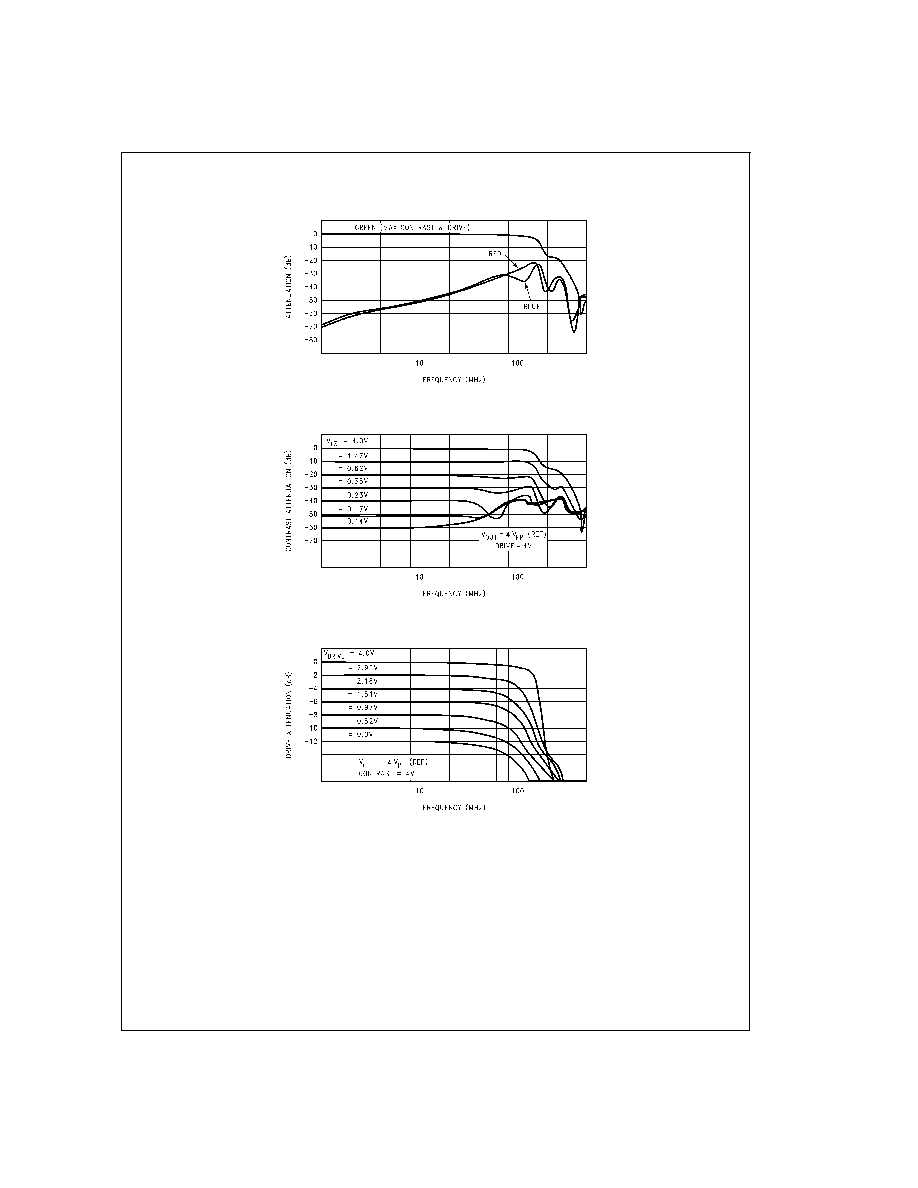
Typical Performance Characteristics
V
CC
= 12V, T
A
= 25∞C unless otherwise specified (Continued)
LM1282 Crosstalk vs Frequency
DS012519-4
LM1282 Contrast vs Frequency
DS012519-5
LM1282 Drive vs Frequency
DS012519-6
5
www.national.com
Timing Diagrams
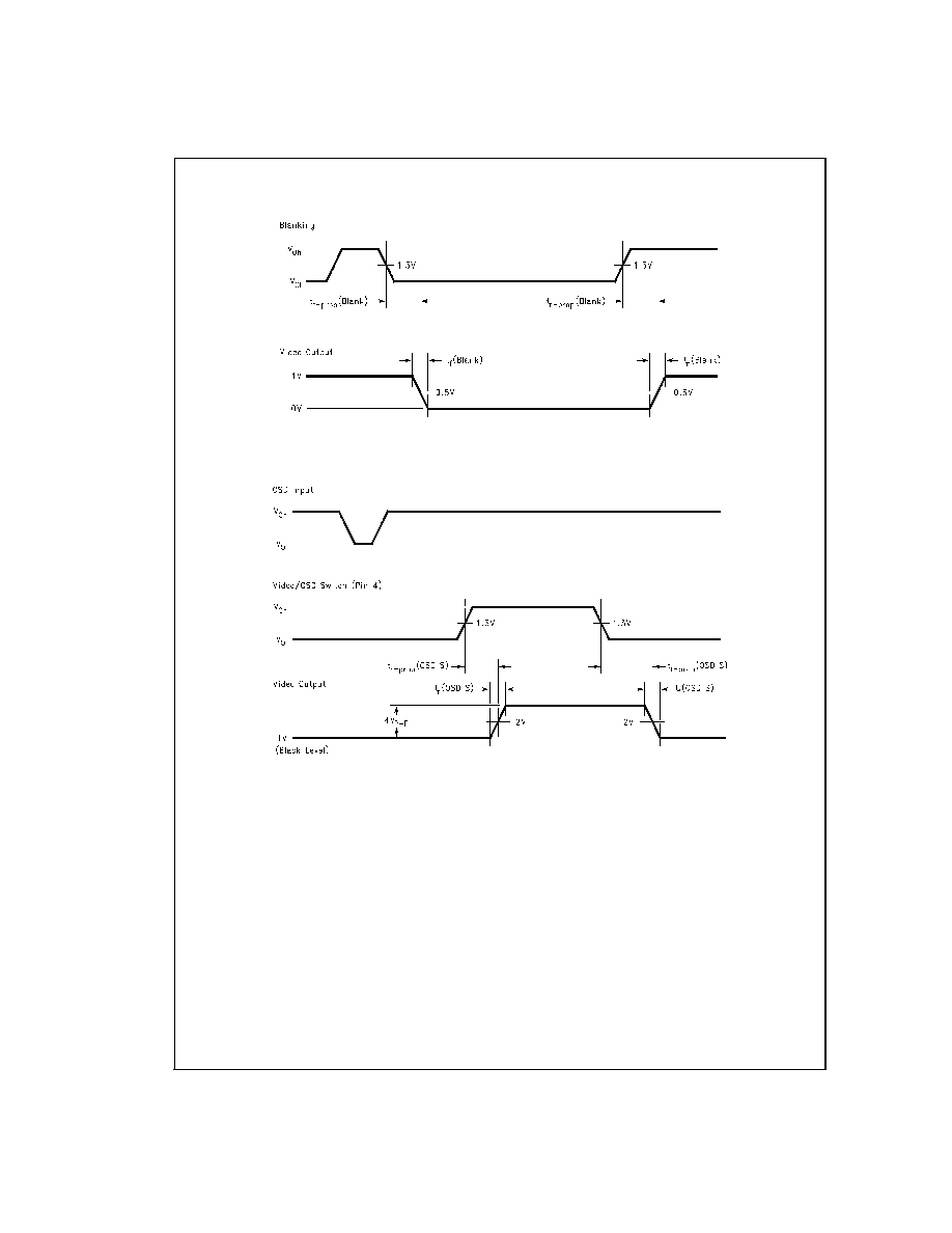
Blanking Propagation Delay and Rise/Fall Time
DS012519-7
FIGURE 2.
Video to OSD, OSD to Video Propagation Delay and Switching Time
DS012519-8
FIGURE 3.
www.national.com
6
Timing Diagrams
(Continued)
Test Circuits
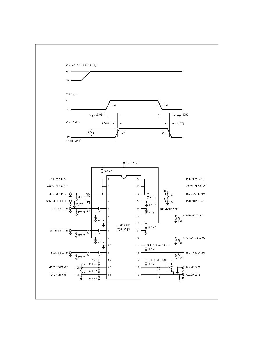
OSD Propagation Delay and Rise/Fall Times
DS012519-9
FIGURE 4.
DS012519-10
FIGURE 5. LM1282 OSD Video Preamp DC Test Circuit
7
www.national.com
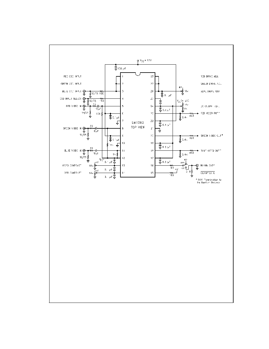
Test Circuits
(Continued)
DS012519-11
FIGURE 6. LM1282 OSD Video Preamp AC Test Circuit
www.national.com
8

Test Circuits
(Continued)
DS012519-12
FIGURE 7. LM1282 OSD Video Preamp Demonstration Board Schematic
9
www.national.com
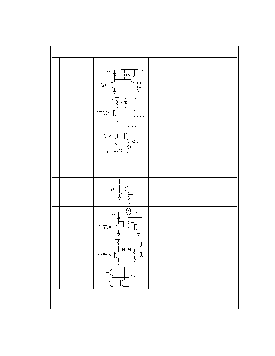
Pin Descriptions
Pin
Pin
Schematic
Description
No.
Name
1
2
3
Red OSD Input
Green OSD Input
Blue OSD Input
These inputs accept standard TTL inputs. Each color is either
fully on (logic high) or fully off (logic low). Connect unused
pins to ground with a 47k resistor.
4
Video/OSD Switch
This input accepts a standard TTL input.
H = OSD
L = Video
Connect to ground with a 47k resistor when not using OSD.
5
8
11
Red Video In
Green Video In
Blue Video In
Video inputs. These inputs must be AC Coupled with a
minimum of a 1 µF cap, 10 µF is perferred. DC restoration is
done at these inputs. A series resistor of about 33
should
also be used.
6
9
V
CC1
Power supply pins (excluding output stage)
7
10
21
Ground
Ground pins. All grounds are internally connected and must
also be connected on the PCB.
12
V
REF
Pin used for additional filter capacitor to internal reference.
The voltage at this pin is 2.0V.
13
14
26
27
28
Video Contrast
OSD Contrast
Blue Drive
Green Drive
Red Drive
Contrast control pins:
4V -- no attenuation
0V -- over 60 dB attenuation
Drive control pins:
4V -- no attenuation
0V -- 12 dB attenuation
15
16
Clamp Gate
Blank Gate
Both pins accept TTL inputs and are active low. The clamp
gate provides DC restoration of the video signal. The blank
gate forces the video outputs to below 200 mV.
17
19
24
Blue Clamp Cap
Green Clamp Cap
Red Clamp Cap
The external clamp cap is charged and discharged to the
correction voltage needed for DC restoration. 0.1 µF is the
recommended value.
www.national.com
10

Pin Descriptions
(Continued)
Pin
Pin
Schematic
Description
No.
Name
18
20
23
Blue Video Out
Green Video Out
Red Video Out
Video output. For proper black level the output must drive
390
impedance.
22
V
CC2
Power supply pin for the output stage. There are no internal
connections to V
CC1
.
25
RGB Cutoff Adjust
Sets the black level of the video outputs to all three
channels. Range is 0V to 4V. Minimum black level is limited
to about 300 mV.
Functional Description
Figure 1 on the front page shows the block diagram of the
LM1282 along with the pinout of the IC. Each channel re-
ceives both a video signal and an OSD signal at its input am-
plifier (-A1). The Video/OSD Switch signal also goes to the
input amplifiers, controlling whether the video or the OSD
signal passes through the LM1282. Both the OSD inputs and
the Video/OSD Switch accept standard TTL signals. If video
is selected then a TTL low is applied to pin 4, for OSD a TTL
high needs to be applied. When the OSD feature is not used,
then pin 4 needs to be connected to ground via a 47k resis-
tor. Although the OSD input signal is a TTL signal, the input
amplifier processes this signal to match the video levels. A
TTL high signal will be at the video white level and a TTL low
signal will typically be within 100 mV of the video black level.
Note that by using the LM1282 the monitor designer con-
nects the OSD input signals directly to the IC with NO signal
processing.
DC restoration is performed on the video inputs to the
LM1282. Remember video inputs are always AC coupled to
the video pre-amp. There is no DC standard for the video in-
put, therefore AC coupling the video inputs is necessary for
proper operation of the monitor. A minimum capacitance of 1
µF is recommended at the video input pins. The preferred
value is 10 µF. Part of the signal processing of the TTL OSD
inputs is matching the black level of the OSD signal (TTL
low) to the black level of the video signal. With AC coupling
of the video inputs, DC restoration must be done at the input
to perform the black level matching.
The next stage in the LM1282 is the Contrast Attenuation.
Both the video and OSD contrast controls go to this stage.
For easy interfacing to 5V DACs all control inputs, including
these two controls, use a 0V to 4V range. Both contrast con-
trols give no attenuation at 4V and full attenuation (over -50
dB) at 0V. The video and OSD contrast adjustments are
completely independent of each other, allowing the user to
set the desired contrast of the OSD window without affecting
the video portion of the display. There is only one output from
this section, any adjustments on the signal path beyond the
contrast stage affects both the video signal and the OSD sig-
nal.
Following the Contrast Attenuation block is the Drive Attenu-
ation. By having the Drive Attenuation past the contrast
stage, any adjustment made on the video signal will equally
affect the OSD signal. This configuration simplifies the white
level adjustment. When the white level of the video is ad-
justed then the OSD white level is automatically set. The
only OSD adjustment necessary when using the LM1282 is
the OSD contrast. Note that when performing the white level
adjustments the video portion of the display must be used,
because there are minor variations between the OSD levels
and the video levels.
The output stage is the -A2 amplifier. This stage is similar to
the LM1205 output stage, where the video output can be
blanked to a level below the video black level. A blacker than
black output during blanking provides the capability to blank
at the cathodes of the CRT. This eliminates the need for us-
ing high voltage transistors at G1 of the CRT to perform the
blanking function. When the outputs are blanked the
LM1282 can still DC restore the video output signal by using
the Clamp Gate. There is an internal feedback stage that
does the DC restoration. In order to maintain the correct
video levels based on this feedback loop, the video output of
the LM1282 must be terminated with a 390
impedance.
The required correction voltage for DC restoration is stored
on the clamp cap. A value of 0.1 µF is recommended for the
clamp cap. If the cap value is too small then there will be a tilt
(shift) in the DC level of the video output during the horizon-
tal scan. If the cap value is too large, then the DC restoration
circuit may not be able to maintain the proper DC level of the
video signal. Since DC restoration is also done at the video
inputs, larger clamp cap values will be less of a problem with
the LM1282 than with most other video preamps. The refer-
ence level for the DC restoration circuit is set at the RGB
Cutoff Adjust pin (pin 25). Most monitor applications AC
11
www.national.com

Functional Description
(Continued)
couple the preamp output to the cathode drivers. Therefore
only one cutoff adjustment is provided, this is used primarily
to optimize the operation of the cathode drivers.
Note that the Blank and Clamp Gates are active low. These
pins are normally controlled by standard TTL signals. For
video applications the Clamp Gate must be used. There are
designs where the blank function may not be required. When
the Blank Gate is not used, it must be tied high by a pullup
resistor. A resistor value of 47k is acceptable, going to either
4V or 12V.
Gain of -A2 is controlled by the Drive Adjust pins. These are
also 0V to 4V control voltages. 4V results in no attenuation at
-A2, and 0V results in a -12 dB attenuation. The 12 dB ad-
justment range should provide more than enough adjust-
ment for setting the white level. Note that a 12 dB range
gives a 4 to 1 range in the output levels between the three
channels.
Applications of the LM1282
A schematic for a demonstration board is shown in
Figure 7.
This board was used for the characterization of the LM1282.
Note that a 33
resistor is in series with all inputs to the IC
that receive external signals. These resistors are recom-
mended to protect the IC from any sudden voltage surges
that may result during the power up and power down modes,
or when connecting the monitor to other equipment. The
monitor designer should include these resistors in his de-
sign. If additional protection against ESD at the video inputs
is necessary, then adding clamp diodes on the IC side of the
33
resistor is recommended; one to V
CC1
and one to
ground. Normally a designer may want to increase the value
of the 33
resistor at pins 5, 8, and 11 for additional ESD
protection at the video inputs. Remember that the input ca-
pacitor to the video inputs is also part of the DC restoration
circuit. This circuit is depending on a maximum circuit resis-
tance of about 110
. The 33
resistors should not be in-
creased in value. The internal ESD protection and the exter-
nal clamp diodes, one to +12V and the other to ground, will
provide excellent ESD protection.
Interfacing to the OSD inputs is quite easy since the signal
processing necessary to match the OSD signals to the video
levels is done internally by the LM1282. However, proper de-
sign techniques must be followed in assuring that a good
TTL signal is received at the LM1282. Ground bounce in the
TTL signal can cause improper switching times, possibly
with multiple switching. Such affects will result in degradation
in the quality of the displayed OSD window. The final TTL
stage needs to be located near the LM1282 to assure clean
TTL signals. Propagation delay is another source capable of
degrading the OSD display. The optimum condition is to
have all OSD signals originate from one register, keeping the
variation in the propagation delays under 5 ns. If the OSD
feature is not used, or the lines may be disconnected for
some testing operations, then the Video/OSD Switch pin (pin
4) must have a pull down resistor to ground to insure opera-
tion in the video mode. Using a 47k pull down resistor will
keep this pin low, and provide enough resistance to where
the pin can still be driven directly by a TTL signal. Pins 1
through 3 should also be terminated the same way, eliminat-
ing the potential to switch logic levels just from the noise at
the open pins.
Figures 2, 3, 4 show the timing diagrams for the LM1282.
When measuring propagation delays all TTL signals are
measured at the time they cross 1.3V. The video output is set
to 4 V
PP
. Propagation delay is measured when the output is
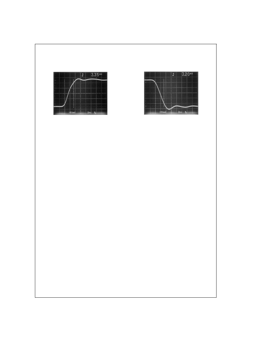
half way in its transition (changed by 2V). Rise and fall times
of the video output are measured between the 10% and 90%
points of the transitions.
Board layout is always critical in a high frequency application
such as using the LM1282. A poor layout can result in ringing
of the video waveform after sudden transitions, or the part
could actually oscillate. A good ground plane and proper
routing of the +12V are important steps to a good PCB lay-
out. The LM1282 can operate on a single sided board with a
good layout. A ground plane is recommended and it is best to
isolate the output stage grounds from the rest of the circuit.
Also the two grounds should be connected together only at
one point, ideally where the ground cable is connected to the
board ground. Yes, all grounds are connected internally, but
trace resistance can still allow for ground bounce, giving
enough feedback for oscillations. The output stage power
supply pin, pin 22, does not have an internal connection to
the other power supply pins. This pin must be connected to
the +12V supply, preferably with high frequency isolation.
This is easily done with a ferrite bead between pin 22 and the
+12V supply.
Figure 8 and Figure 9 show the waveform ob-
tained with the LM1282 using the single sided demo board
designed for this part.
www.national.com
12
References
Zahid Rahim, "Guide to CRT Video Design," Application Note 861, National Semiconductor Corp., Jan. 1993
Ott, Henry W.
Noise Reduction Techniques in Electronic systems , John Wiley & Sons, New York, 1976
DS012519-22
FIGURE 8. LM1282 Rise Time
DS012519-23
FIGURE 9. LM1282 Fall Time
13
www.national.com
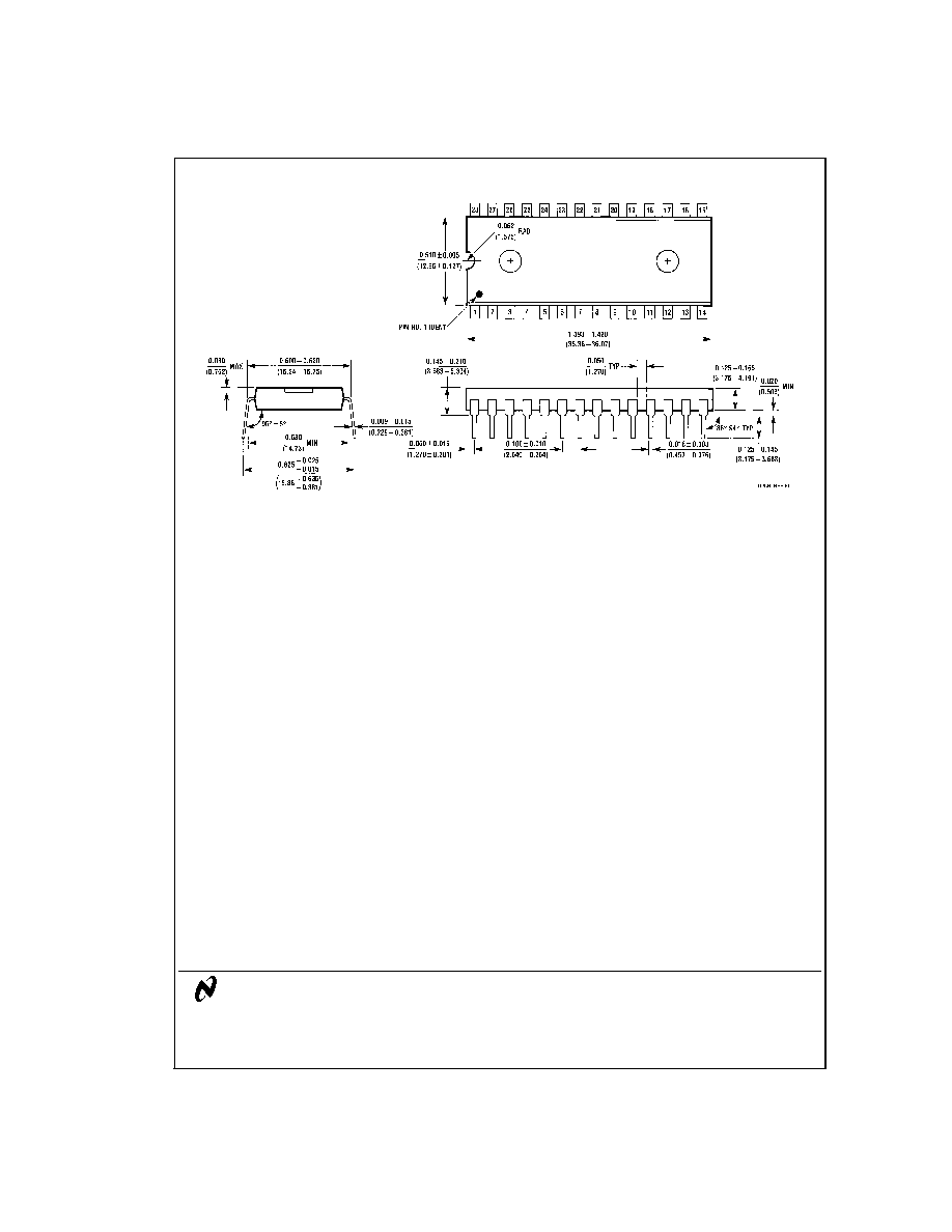
Physical Dimensions
inches (millimeters) unless otherwise noted
LIFE SUPPORT POLICY
NATIONAL'S PRODUCTS ARE NOT AUTHORIZED FOR USE AS CRITICAL COMPONENTS IN LIFE SUPPORT DE-
VICES OR SYSTEMS WITHOUT THE EXPRESS WRITTEN APPROVAL OF THE PRESIDENT OF NATIONAL SEMI-
CONDUCTOR CORPORATION. As used herein:
1. Life support devices or systems are devices or sys-
tems which, (a) are intended for surgical implant into
the body, or (b) support or sustain life, and whose fail-
ure to perform when properly used in accordance
with instructions for use provided in the labeling, can
be reasonably expected to result in a significant injury
to the user.
2. A critical component in any component of a life support
device or system whose failure to perform can be rea-
sonably expected to cause the failure of the life support
device or system, or to affect its safety or effectiveness.
National Semiconductor
Corporation
Americas
Tel: 1-800-272-9959
Fax: 1-800-737-7018
Email: support@nsc.com
www.national.com
National Semiconductor
Europe
Fax: +49 (0) 1 80-530 85 86
Email: europe.support@nsc.com
Deutsch Tel: +49 (0) 1 80-530 85 85
English
Tel: +49 (0) 1 80-532 78 32
FranÁais Tel: +49 (0) 1 80-532 93 58
Italiano
Tel: +49 (0) 1 80-534 16 80
National Semiconductor
Asia Pacific Customer
Response Group
Tel: 65-2544466
Fax: 65-2504466
Email: sea.support@nsc.com
National Semiconductor
Japan Ltd.
Tel: 81-3-5620-6175
Fax: 81-3-5620-6179
28-Lead (0.600" Wide) Molded Dual-In-Line Package
NS Package Number N28B
LM1282
1
10MHz
RGB
V
ideo
Amplifier
System
with
On
Screen
Display
(OSD)
National does not assume any responsibility for use of any circuitry described, no circuit patent licenses are implied and National reserves the right at any time without notice to change said circuitry and specifications.