 | –≠–ª–µ–∫—Ç—Ä–æ–Ω–Ω—ã–π –∫–æ–º–ø–æ–Ω–µ–Ω—Ç: LM1290N | –°–∫–∞—á–∞—Ç—å:  PDF PDF  ZIP ZIP |
LM1290
Autosync Horizontal Deflection Processor
General Description
The LM1290 is a high-performance, low-cost deflection solu-
tion for autosync monitors.
The LM1290 provides full autosync capability, DC controls
and complete freedom from manufacturing trims. Its continu-
ous capture range is from 22 kHz to 110 kHz (1:5). Mode
change frequency ramping, for protection of the horizontal
deflection output transistor, is programmable by using an ex-
ternal capacitor.
Together with the National Semiconductor LM1296 Raster
Geometry Correction System for Multi-Frequency Displays,
excellent performance is offered. The two-chip solution pro-
vides the advantage of good jitter performance, simplified
board layout, and lower system cost.
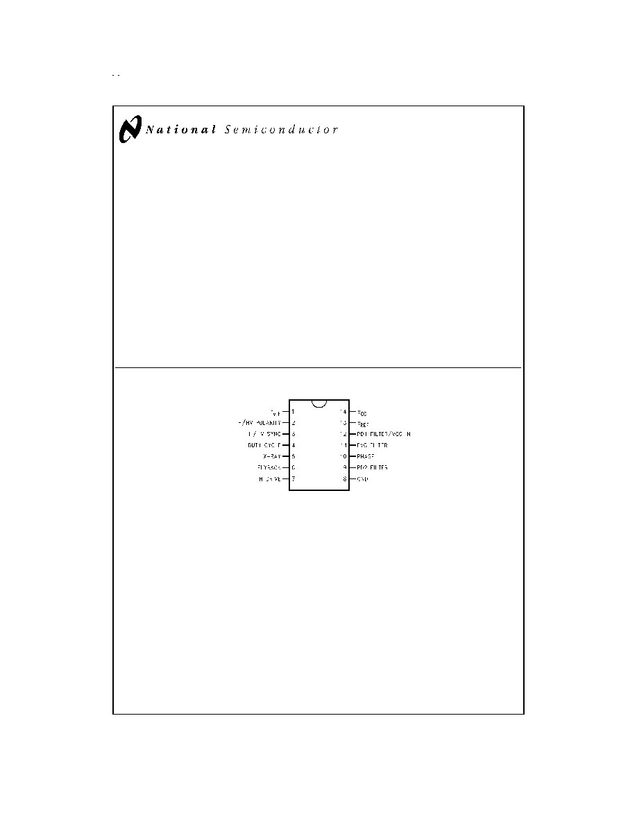
The LM1290 is packaged in a 14-pin plastic DIP package.
Features
n
Full autosync -- 22 kHz to 110 kHz with no component
switching or external adjustments
n
No manufacturing trims needed -- internal VCO
capacitor trimmed on chip
n
Sample-and-hold circuit for fast top-of-screen phase
recovery, even when using composite sync
n
DC-controlled H phase and duty cycle
n
Resistor-programmable minimum VCO frequency
n
Excellent jitter performance
n
X-ray input disables H drive until V
CC
powered down
n
Low V
CC
disables H drive (V
CC
<
8.5V)
n
H output transistor protected against accidental turn on
during flyback
n
Capacitor-programmable frequency ramping, d
f
VCO
/ dt,
protects H output transistor during scanning mode
changes
Connection Diagram
DS012917-1
FIGURE 1.
Order Number LM1290N
See NS Package Number N14A
January 1997
LM1290
Autosync
Horizontal
Deflection
Processor
© 1999 National Semiconductor Corporation
DS012917
www.national.com
Absolute Maximum Ratings
(Notes 1, 3)
If Military/Aerospace specified devices are required,
please contact the National Semiconductor Sales Office/
Distributors for availability and specifications.
Supply Voltage (V
CC
)
15V
Input Voltage (V
DC
)
Pin 1
8V
Pins 3, 4, 5, 6
V
CC
Pin 10
1.0V
<
V
DC
<
7.5V
Pin 12
10V
Output Sink Current, Pin 7
130 mA
Power Dissipation (P
D
)
(Above 25∞C, derate based on
JA
and T
J
)
1.65W
Thermal Resistance (
JA
)
75∞C/W
Junction Temperature (T
J
)
150∞C
ESD Susceptibility (Note 5)
3.5 kV
Storage Temperature
-65∞C to +150∞C
Lead Temperature
(Soldering 10 seconds)
265∞C
Operating Ratings
(Note 2)
Operating Temperature Range
-20∞C to +80∞C
Supply Voltage
10.8V
V
CC
13.2V
Electrical Characteristics
See Test Circuit (
Figure 2) ; T
A
= 25∞C; V
CC
= 12V; V
5
= 0V unless otherwise stated.
Parameter
Condition
Typical
Limit
Units
(Note 6)
(Note 7)
Supply Current (Pin 14)
Pin 3 and Pin 7 Open Circuit,
30
40
mA (max)
Pin 1 = -100 µA
Minimum Capture Frequency
H Sync Duty Cycle = 10%;
10
22
kHz (max)
Maximum Capture Frequency
Pin 1 (f
MIN
) Open
115
110
kHz (min)
H/HV SYNC Input (Pin 3)
High Level
2.2
V (min)
Threshold Voltage
Low Level
0.8
V (max)
H/HV SYNC Input (Pin 3)
26
24
%
Maximum Sync Tip Duty Cycle
H/HV SYNC Input (Pin 3)
f
H
= 22 kHz
5
%
Minimum Sync Tip Duty Cycle
H/HV POLARITY (Pin 2)
C
POL
= 0.1 µF; I
OL
= +1 µA
0.05
0.4
V (max)
Low Level Output Voltage, V
OL
H/HV POLARITY (Pin 2)
C
POL
= 0.1 µF; I
OL
= -1 µA
4.5
4
V (min)
High Level Output Voltage, V
OH
FVC Gain
22 kHz
f
H
110 kHz
0.055
V/kHz
VCO Gain
22 kHz
f
VCO
110 kHz
18.2
kHz/V
Phase Detector 1 Gain
H Sync Duty Cycle = 10%:
µA/radian
f
H
= 110 kHz
120
f
H
= 60 kHz
80
f
H
= 22 kHz
30
Phase Detector 1 Output Impedance
20
k
(Pin 12)
Phase Detector 1 Leakage Current +
H/HV SYNC Input Grounded
0.3
2
µA
VCO Bias Current (Pin 12)
Jitter
f
H
= 110 kHz (Note 8)
0.9
ns p-p
f
H
= 90 kHz
1.1
f
H
= 60 kHz
1.6
f
H
= 31 kHz
3.6
f
H
= 22 kHz
5.8
Free Run Frequency Variation
I
1
= -225 µA
32
34
kHz (max)
26
25
kHz (min)
H Drive Phase Control Gain
V
10
= 2V to 6V (Note 11)
8.89
% T
H
/V
(32)
(∞/V)
www.national.com
2
Electrical Characteristics
(Continued)
See Test Circuit (
Figure 2) ; T
A
= 25∞C; V
CC
= 12V; V
5
= 0V unless otherwise stated.
Parameter
Condition
Typical
Limit
Units
(Note 6)
(Note 7)
H Drive Phase Control Range
V
10
= 3.6V to 7V (Notes 9, 11)
±
14
%T
H
(See Application Hint #3)
H Drive Duty Cycle Control Gain
V
4
= 0V to 4V (Note 10)
10.8
%/V
H Drive Duty Cycle Maximum (Pin 7)
V
4
= 0V (Note 10)
68
63
% (min)
H Drive Duty Cycle Minimum (Pin 7)
V
4
= 4V (Note 10)
25
35
% (max)
H Drive Low Level Output Voltage (Pin 7)
I
OL
= 100 mA
0.7
V
Flyback Input Threshold Voltage (Pin 6)
Positive-Going Flyback Pulse
2.2
V
Maximum Allowable Storage Delay of
From H Drive Rising Edge to
Horizontal Deflection Output Transistor
Center of Flyback Pulse
30
%T
H
Plus Half of Flyback Pulse Width
V
CC
Lockout Threshold Voltage
V
CC
Below Threshold:
8.5
V (max)
(Pin 14)
H Drive Output Disabled
V
CC
Above Threshold:
10.5
V (min)
H Drive Output Enabled
X-Ray Shutdown Threshold Voltage
Above Threshold:
1.85
2
V (min)
(Pin 5)
H Drive Output Disabled
Note 1: Absolute Maximum Ratings indicate limits beyond which damage to the device may occur.
Note 2: Operating Ratings indicate conditions for which the device is functional, but do not guarantee specific performance limits. For guaranteed specifications and
test conditions, see the Electrical Characteristics. The guaranteed specifications apply only for the test conditions listed. Some performance characteristics may de-
grade when the device is not operated under the listed test conditions.
Note 3: All voltages are measured with respect to GND, unless otherwise specified.
Note 4: The maximum power dissipation must be derated at elevated temperatures and is dictated by T
JMAX
,
JA
and the ambient temperature, T
A
. The maximum
allowable power dissipation at any elevated temperature is P
D
= (T
JMAX
- T
A
)/
JA
or the number given in the Absolute Maximum Ratings, whichever is lower. For
this device, T
JMAX
= 150∞C. The typical thermal resistance (
JA
) of the LM1290N is 75∞C/W.
Note 5: Human Body model, 100 pF capacitor discharged through a 1.5 k
resistor.
Note 6: Typical specifications are at T
A
= 25∞C and represent most likely parametric norm.
Note 7: Tested limits are guaranteed to National's AOQL (Average Outgoing Quality Level).
Note 8: The standard deviation,
, of the flyback pulse period is measured with a HP 53310A Modulation Domain Analyzer. Peak-to-peak jitter of the flyback pulse
is defined by 6
.
Note 9: A positive phase value represents a phase lead of the flyback pulse peak with reference to the center of H sync.
Note 10: The duty cycle is measured under the conditions of free run with I
1
= -100 µA, T
FBP
= 3 µs and T
d
= 3.5 µs where T
FBP
and T
d
are the flyback pulse width
and the turn off delay of the H deflection output transistor respectively.
Note 11: T
H
is defined as the total time of one horizontal line.
www.national.com
3
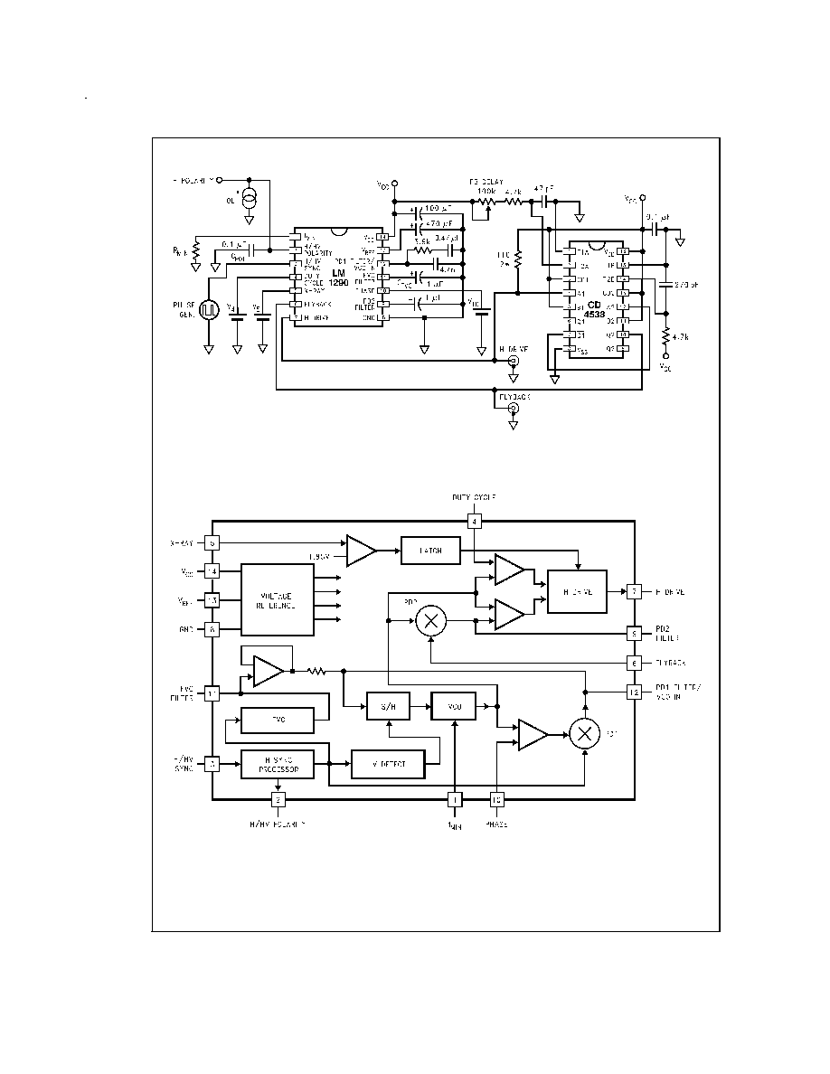
Test Circuit
System Block Diagram
DS012917-2
FIGURE 2.
DS012917-3
FIGURE 3.
www.national.com
4
Pin Descriptions
See
Figure 4 through Figure 10 for input and output sche-
matics.
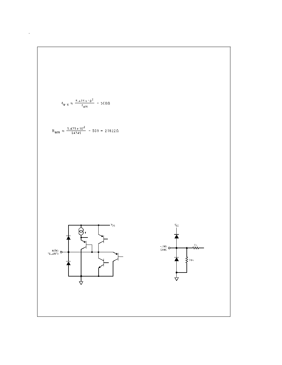
Pin 1 -- f
MIN
: A resistor from this pin to ground sets the free
run frequency of the LM1290. The free run frequency should
be set typically as:
f
MIN
= 0.85(f
MINLOCK
) - 2 kHz
where f
MINLOCK
is the minimum lock frequency required for
the application. The resistance required to set this frequency
is approximately:
For example, to find R
MIN
for VGA which has f
MINLOCK
=
31.469 kHz,
f
MIN
= 0.85(31.469 kHz) - 2 kHz = 24749
Rounding to the closest standard 1% resistor gives R
MIN
=
21.5 k
.
Pin 2 -- H/HV POLARITY: A 0.1 µF capacitor is connected
from this pin to ground for detecting the polarity of H/HV sync
at pin 3. A low logic level at pin 2 indicates active-high H/HV
sync to pin 3, a high level indicates active-low. See
Figure 4
for the output schematic.
Pin 3 -- H/HV SYNC: This input pin accepts DC-coupled H
or composite sync of either polarity. For best noise immunity,
a resistor of 2 k
or less should be connected from this pin
to pin 8 (GND) via a short path. See
Figure 5 for the input
schematic.
Pin 4 -- DUTY CYCLE: A DC voltage applied to this pin sets
the duty cycle of the H DRIVE output (pin 7), with a range of
approximately 30% to 70%. 2V sets the duty cycle to ap-
proximately 50%. See
Figure 6 for the input schematic.
Pin 5 -- X-RAY: This pin is for monitoring CRT anode volt-
age. If the input voltage exceeds an internal threshold, H
DRIVE output (pin 7) is latched high. V
CC
has to be reduced
to below approximately 2V to clear the latched condition, i.e.,
power must be turned off. See
Figure 7 for the input sche-
matic.
Pin 6 -- FLYBACK: Input pin for phase detector 2. For best
operation, the flyback peak should be at least 5V but not
greater than V
CC
. Any pulse width greater than 1.5 µs is ac-
ceptable. See
Figure 8 for the input schematic.
Pin 7 -- H DRIVE: This is an open-collector output which
provides the drive pulse for the high power deflection circuit.
The pulse duty cycle is controlled by pin 4. Polarity conven-
tion: Horizontal deflection output transistor is on when H
DRIVE OUT is low. See
Figure 9 for the output schematic.
Pin 8 -- GND: System ground. For best jitter performance,
all bypass capacitors should be connected to this pin via
short paths.
Pin 9 -- PD2 FILTER: The low-pass filter cap of between
0.01 µF to 1 µF for the output of phase detector 2 is con-
nected from this pin to pin 8 (GND) via a short path. A
smaller value increases the response.
Pin 10 -- PHASE: A DC control voltage applied to this pin
sets the phase of the flyback pulse with respect to the center
of H sync. See
Figure 10 for the input schematic.
Pin 11 -- FVC FILTER: A 1 µF capacitor is connected from
this pin to pin 8 (GND) via a short path.
Pin 12 -- PD1 OUT/VCO IN: Phase detector 1 has a gated
charge pump output which requires an external low-pass fil-
ter. For best jitter performance, the filter should be grounded
to pin 8 (GND) via a short path. If a voltage source is applied
to this pin, the phase detector is disabled and the VCO can
be controlled directly.
Pin 13 -- V
REF
: This is the decoupling pin for the internal
8.2V reference. It should be decoupled to pin 8 (GND) via a
short path with a cap of at least 470 µF. Do not load this pin.
Pin 14 -- V
CC
: 12V nominal power supply pin. This pin
should be decoupled to pin 8 (GND) via a short path with a
cap of at least 47 µF.
Input/Output Schematics
DS012917-4
FIGURE 4.
DS012917-5
FIGURE 5.
www.national.com
5