 | –≠–ª–µ–∫—Ç—Ä–æ–Ω–Ω—ã–π –∫–æ–º–ø–æ–Ω–µ–Ω—Ç: LM1292 | –°–∫–∞—á–∞—Ç—å:  PDF PDF  ZIP ZIP |
LM1292
Video PLL System for Continuous-Sync Monitors
General Description
The LM1292 is a very low jitter, integrated horizontal time
base solution specifically designed to operate in high perfor-
mance, continuous-sync video monitors. It automatically
synchronizes to any H frequency from 22 kHz to 125 kHz
and provides the drive pulse to the high power deflection cir-
cuit.
Available sync processing includes a vertical sync separator
and a composite video sync stripper. An internal sync selec-
tion scheme gives highest priority to separate H and V sync,
then composite sync, and finally sync on video; no external
switching between sync sources is necessary. The LM1292
provides polarity-normalized H/HV and V sync outputs.
The
LM1292
design
uses
an
on-chip
FVC
(Frequency-to-Voltage Converter) to set the center fre-
quency of the VCO (Voltage-Controlled Oscillator). This
technique allows autosync operation over the entire fre-
quency range using just one optimized set of external com-
ponents.
The system includes a second phase detector which com-
pensates for storage time variation in the horizontal output
transistor; the picture's horizontal position is thus indepen-
dent of temperature and component variance.
The LM1292 provides DC control pins for H Drive duty cycle
and flyback phase.
Features
n
Wide continuous autosync range -- 22 kHz≠125 kHz
(1:5.7) with no component switching or external
adjustments
n
No manufacturing trims required -- internal VCO
capacitor trimmed on chip
n
No costly high-precision components needed
n
Very low phase jitter (below 800 ps at 125 kHz)
n
DC controlled H phase and duty cycle
n
Video mute pulse for blanking during H frequency
transitions
n
Input sync prioritization
n
Clamp pulse position and width control
n
Continuous clamp pulse output, even with no sync input
n
Resistor-programmable minimum and maximum VCO
frequency
n
X-ray input disables H drive and mutes video until V
CC
powered down
n
H drive disabled for V
CC
<
9.5V
n
Horizontal output transistor protected against accidental
turn-on during flyback
n
Capacitor-programmable frequency ramping, d
f
vco
/d
t,
protects H output transistor during scanning mode
changes
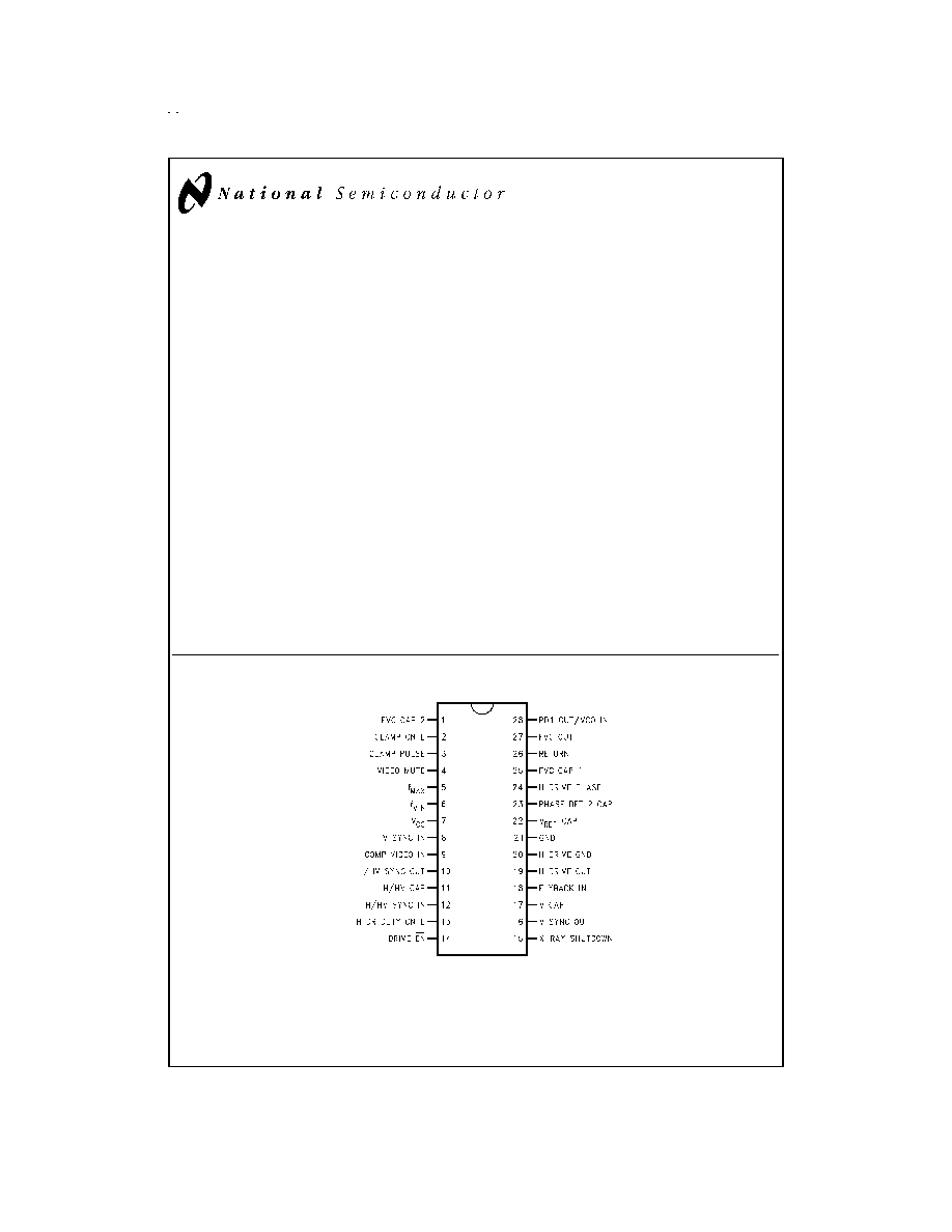
Connection Diagram
DS012844-1
FIGURE 1. Order Number LM1292N
See NS Package Number N28B
April 1999
LM1292
V
ideo
PLL
System
for
Continuous-Sync
Monitors
© 1999 National Semiconductor Corporation
DS012844
www.national.com
Absolute Maximum Ratings
(Notes 1, 3)
If Military/Aerospace specified devices are required,
please contact the National Semiconductor Sales Office/
Distributors for availability and specifications.
Supply Voltage
14V
Input Voltage, V
DC
Pin 14
Pin 24
Pins 5, 6
Pins 8, 28
Pins 2, 9, 12, 13, 15, 18
5V
1.3V
<
V
IN
<
7.2V
8V
10V
V
CC
Power Dissipation (P
D
)
2.5W
(Above 25∞C, derate based on
JA
and T
J
)
Thermal Resistance (
JA
)
50∞C/W
Junction Temperature (T
J
)
150∞C
ESD Susceptibility (Note 5)
2 kV
Storage Temperature
-65∞C to +80∞C
Lead Temperature
(Soldering 10 sec.)
265∞C
Operating Ratings
(Note 2)
Operating Temperature Range
-20∞C to +80∞C
Supply Voltage
10.8V
V
CC
13.2V
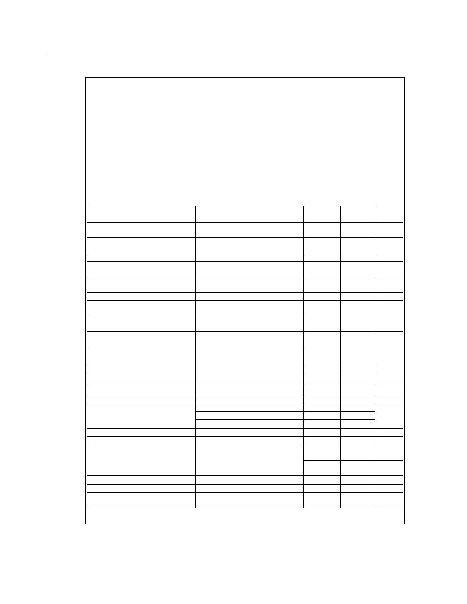
Electrical Characteristics
See Test Circuit (
Figure 2); T
A
= 25∞C; V
CC
= 12V; V
14
= 0V; V
15
= 0V unless
otherwise stated
Parameter
Conditions
Typical
(Note 6)
Limit
(Note 7)
Units
Supply Current
30
41
mA
(max)
Minimum Composite Video
Input Amplitude (Pin 9)
Cap Coupled (0.01 µF), Sync Tip to
Black Level
0.14
V
PP
DC Clamp Level, Composite Video Input
2.0
V
Clamp Charging Current, Composite
Video Input
6
mA
Minimum H/HV Sync Input Amplitude
(Pin 12)
Cap Coupled, 10% Duty Cycle (Note 8)
1.0
V
PP
Minimum V Sync Input Amplitude (Pin 8)
Cap Coupled, 1% Duty Cycle
1.0
V
PP
High Level Output Voltage V
OH
(Pins 10,
16)
I
OH
= -100 µA
4.3
3.8
V (Min)
Low Level Output Voltage V
OL
(Pins 10,
16)
I
OL
= 1.6 mA
0.25
0.4
V (Max)
Video Mute Low Level Output Voltage
(Pin 4)
I
OL
= 2 mA
0.4
V (Max)
Mute Detection Voltage Threshold
V, | FVC Cap 1 - FVC Cap 2 | for Mute
Output Low
100
mV
Flyback Input Threshold (Pin 18)
Positive Going Flyback Pulse
1.4
V
Under-Voltage Lockout (Pin 7)
V
CC
Below Threshold: H Drive Output
Open (Unlatched)
10.8
V
Frequency to Voltage Gain
22 kHz
f
H
125 kHz
0.047
V/kHz
VCO Gain Constant
f
VCO
= 100 kHz
1.34 x 10
5
Rad/s/V
PD1 Phase Detector Gain Constant
f
VCO
= 100 kHz
130
µA/Rad
f
VCO
= 60 kHz
78.1
f
VCO
= 22 kHz
28.6
Frequency to Voltage Linearity
22 kHz
f
H
125 kHz
1.0
%
VCO Linearity
22 kHz
f
VCO
125 kHz
1.0
%
Jitter
f
H
= 30 kHz (Note 9)
f
H
= 60 kHz
3.25
1.45
ns p-p
f
H
= 100 kHz
f
H
= 125 kHz
895
763
ps p-p
H Drive Duty Cycle Control Gain
V
13
= 0V≠4V; 30%≠70% Allowed
0.11
T
H
/V
H Drive Phase Control Gain
V
24
= 1.5V≠7V (Note 10)
32
∞/V
PD1 Phase Detector Leakage Current
+ VCO Input Bias Current (Pin 28)
1
µA
www.national.com
2

Electrical Characteristics
See Test Circuit (
Figure 2); T
A
= 25∞C; V
CC
= 12V; V
14
= 0V; V
15
= 0V unless
otherwise stated (Continued)
Parameter
Conditions
Typical
(Note 6)
Limit
(Note 7)
Units
H Drive Low Level Output Voltage (Pin
19)
I
OL
= 100 mA
0.7
V
H Drive EN Low Level Input Voltage (Pin
14)
H Drive Output Active
0.8
V (Max)
H Drive EN High Level Input Voltage (Pin
14)
H Drive Output Open (Unlatched)
2.0
V (Min)
X-Ray Shutdown Threshold Voltage (Pin
15)
V
15
Above Threshold, H Drive
Output Open (Latched)
1.8
1.7
1.9
V (Min)
V (Max)
H/HV Sync Out Propagation Delay
Change
H/HV In vs Comp Video In
32
ns
Clamp Pulse Width
(Back Porch)R
SET
= 15 k
; V
SET
= 0V
0.4
µs
(Back Porch)R
SET
= 15 k
; V
SET
= 1.5V
1.4
µs
(Sync Tip)R
SET
= 15 k
; V
SET
= 4V
0.6
µs
Clamp Pulse Delay
(Back Porch) Trailing Edge H/HV Sync
In to Leading Edge Clamp Pulse
0.1
µs
(Sync Tip) Leading Edge H/HV Sync In
to Leading Edge Clamp Pulse
0.025 T
H
s
Note 1: Absolute Maximum Ratings indicate limits beyond which damage to the device may occur.
Note 2: Operating Ratings indicate conditions for which the device is functional, but do not guarantee specific performance limits. For guaranteed specifications and
test conditions, see the Electrical Characteristics. The guaranteed specifications apply only for the test conditions listed. Some performance characteristics may de-
grade when the device is not operated under the listed test conditions.
Note 3: All voltages are measured with respect to GND, unless otherwise specified.
Note 4: The maximum power dissipation must be derated at elevated temperatures and is dictated by T
JMAX
,
JA
and the ambient temperature, T
A
. The maximum
allowable power dissipation at any elevated temperature is P
D
= (T
JMAX
- T
A
)/
JA
or the number given in the Absolute Maximum Ratings, whichever is lower. For
this device, T
JMAX
= 150∞C. The typical thermal resistance (
JA
) of these parts when board mounted follow: LM1292N 50∞C/W.
Note 5: Human Body model, 100 pF capacitor discharged through a 1.5 k
resistor.
Note 6: Typical specifications are at T
A
= 25∞C and represent most likely parametric norm.
Note 7: Tested limits are guaranteed to National's AOQL (Average Outgoing Quality Level).
Note 8: The typical duty cycle range allowed for the H sync tip is from 5%≠26%.
Note 9: The standard deviation,
, of the flyback pulse period is measured with HP 53310A Modulation Domain Analyzer. Peak-to-peak jitter of the flyback pulse is
defined by 6
.
Note 10: Phase Limits:
,
expressed as a fraction of the horizontal period T
H
, where T
DFB
is the horizontal output transistor turn-off delay from the rising edge of H Drive to the FBP peak. A
positive phase value represents a phase lead of the FBP peak with reference to the leading edge of H sync.
www.national.com
3

Test Circuit
DS012844-2
FIGURE
2.
www.national.com
4
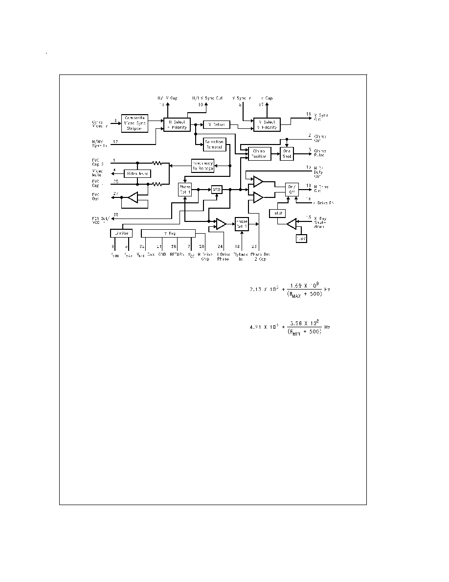
Block Diagram
Pin Descriptions
See
Figure 4 through Figure 14 for input and output sche-
matics.
Pin 1 -- FVC CAP 2: Secondary FVC filter pin. C
FVC2
is con-
nected from this pin to ground. The width of the VIDEO
MUTE (pin 4) pulse is controlled by the time constant differ-
ence between the filters at pins 1 and 25.
Pin 2≠CLAMP CNTL: This low-impedance current-mode in-
put pin is internally biased to 2V. The direction of current sets
the pulse position (back porch or sync-tip), while the current
magnitude sets the pulse width. In a typical application, a
control voltage of 0V≠4V is applied to this pin through a
15 k
resistor. A voltage below 2V positions the pulse on the
back porch of the horizontal sync pulse and decreasing volt-
age narrows the pulse. A voltage above 2V sets the pulse on
the H sync-tip (slightly delayed from the leading edge) and
increasing voltage narrows the pulse. At the boundary of the
switchover between the two modes, there is a narrow region
of uncertainty resulting in oscillation, which should be no
problem in most applications.
When there is no H sync in sync-tip mode, the clamp pulse
is generated by the VCO at the frequency preset by pin 6
(f
MIN
). This feature is intended for use in On Screen Display
systems.
Pin 3 -- CLAMP PULSE: Active-low clamp pulse output.
See
Figure 4 for the output schematic.
Pin 4 -- VIDEO MUTE: This NPN open-collector output pro-
duces an active-low pulse when triggered by a step change
of H sync frequency. See
Figure 5 for the output schematic.
Pin 5 -- f
MAX
: A resistor from this pin to ground sets the up-
per frequency limit of the VCO. f
MAX
is approximately:
Pin 6 -- f
MIN
: A resistor from this pin to ground sets the lower
frequency limit of the VCO. f
MIN
is approximately:
Pin 7 -- V
CC
: 12V nominal power supply pin. This pin should
be decoupled to pin 21 (GND) via a short path with a cap of
at least 47 µF.
Pin 8 -- V SYNC IN: This pin accepts AC-coupled V sync of
either polarity. The pin is internally biased at 5.2V; its input
resistance is approximately 50 k
. For best noise immunity,
a resistor of 2 k
or less should be connected from the input
side of the coupling cap to pin 21 (GND) via a short path.
See
Figure 6 for the input schematic.
Pin 9 -- COMP VIDEO IN: The composite video sync strip-
per is active only when no signal is present at pin 12 (H/HV
IN). The signal to pin 9 must have negative-going sync tips
which are at least 0.14V below black level. For best noise im-
munity, a resistor of 2 k
or less should be connected from
the input side of the coupling cap to pin 21 (GND) via a short
path. See
Figure 7 for the input schematic.
Pin 10 -- H/HV SYNC OUT: The sync processor outputs
active-low H/HV sync derived from the active sync input (pin
9 or pin 12). Pin 10 stays low in the absence of sync input.
See
Figure 4 for the output schematic.
Pin 11 -- H/HV CAP: A capacitor is connected from this pin
to ground for detecting the polarity and existence of H/HV
sync at pin 12.
Pin 12 -- H/HV SYNC IN: This pin accepts AC-coupled H or
composite sync of either polarity. For best noise immunity, a
DS012844-3
FIGURE 3.
www.national.com
5