 | –≠–ª–µ–∫—Ç—Ä–æ–Ω–Ω—ã–π –∫–æ–º–ø–æ–Ω–µ–Ω—Ç: LM1296 | –°–∫–∞—á–∞—Ç—å:  PDF PDF  ZIP ZIP |
LM1296
Raster Geometry Correction System for Multi-Frequency
Displays
General Description
The LM1296 is a monolithic IC for use in the raster scanning
circuitry of a multi-frequency CRT monitor. The IC provides
an S-corrected sawtooth waveform and a variable DC output
voltage. These two outputs drive the vertical deflection am-
plifier. It also provides another waveform for East-West ge-
ometry correction which includes pincushion, corner, and
trapezoid controls. The geometry correction is controlled by
DC input voltages from 0V to 4V.
The raster height and the raster vertical position can be con-
trolled by two DC voltage input pins that adjust the sawtooth
waveform amplitude and the variable DC output voltage. The
East-West correction of the LM1296 has height tracking and
vertical position tracking capabilities. As the height or posi-
tion of the raster is adjusted the geometry correction is main-
tained by the chip automatically.
The LM1296 is packaged in a 16-pin plastic DIP package.
Features
n
Vertical scanning frequency 50 Hz≠165 Hz
n
Accepts either polarity of V sync
n
DC-controlled correction terms
n
Raster vertical position control
n
Vertical S-correction (linearity) control
n
East-West pincushion control
n
East-West trapezoid control
n
East-West corner control
n
Provides both polarities of correction output
n
East-West correction tracks raster vertical position and
height
n
Compatible with LM1290 and LM1292 horizontal PLL
Applications
n
Vertical deflection of monitors
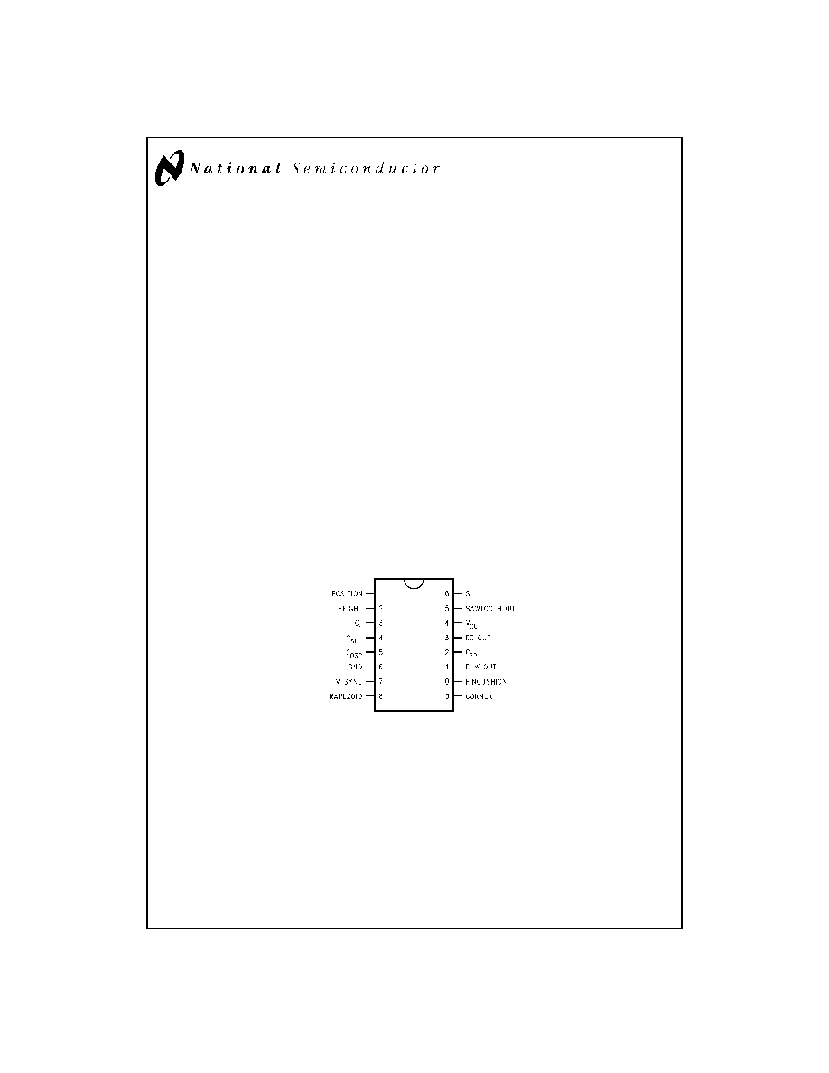
Connection Diagram
DS012894-1
FIGURE 1.
Order Number LM1296N
See NS Package Number N16A
February 1998
LM1296
Raster
Geometry
Correction
System
for
Multi-Frequency
Displays
© 1998 National Semiconductor Corporation
DS012894
www.national.com
Absolute Maximum Ratings
(Notes 3, 1)
If Military/Aerospace specified devices are required,
please contact the National Semiconductor Sales Office/
Distributors for availability and specifications.
Supply Voltage (V
CC
)
15V
Input Voltage (V
IN
)
Pins 1, 2, 8, 9, 10, 16
0V
V
IN
5V
Power Dissipation (P
D
)
Above 25∞C, Derate
Based on
JA
and T
J
(Note 4)
1.5W
Thermal Resistance (
JA
)
81∞C/W
Junction Temperature (T
JMAX
)
150∞C
ESD Susceptibility (Note 5)
2 kV
Storage Temperature
-65∞C to +150∞C
Lead Temperature (Soldering 10 sec.)
265∞C
Operating Ratings
(Note 2)
Supply Voltage (V
CC
)
10.8V
V
CC
13.2V
Input Voltage (V
IN
)
Pins 1, 2, 8, 9, 10, 16
0V
V
IN
4V
Output Current (I
OUT
)
Pins 11, 13, 15
-2 mA
I
OUT
2 mA
Temperature Range (T
A
)
0∞C to +70∞C
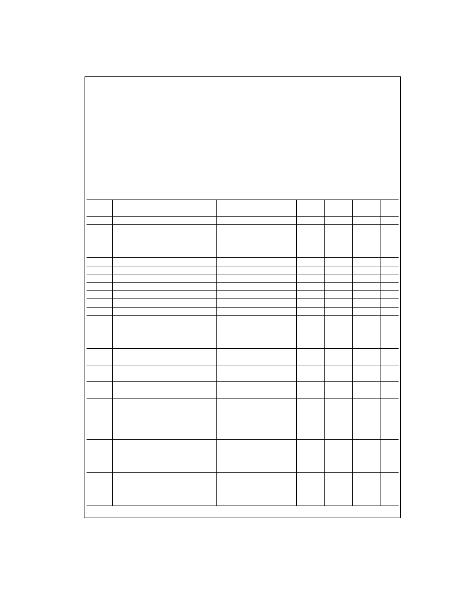
Electrical Characteristics
See Test Circuit (
Figure 2), V
CC
= 12V; V
2
= 4V; V
16
= 4V; V
RDCV
= 0V (Note 6); T
A
= 25∞C unless otherwise specified
Symbol
Parameter
Conditions
Min
Typ
Max
Units
(Note 8)
(Note 7)
(Note 8)
I
CC
Supply Current
Pins 11, 13, 15 Loaded, 2mA
26
32
mA
V SYNC
Vertical Sync Input Sensitivity (Pin 7)
1% or 99% Duty Cycle
Rectangular Waveform
1
V
PP
AC-Coupled to Pin 7
Through 0.01 µF Cap.
f
MIN
Minimum Lock Frequency
C
OSC
= 0.15 µF
50
Hz
f
MAX
Maximum Lock Frequency
C
OSC
= 0.15 µF
165
Hz
f
FR
Free Run Frequency
V
7
= 4V or 0V
40
Hz
R
IN1
Input Resistance (Pin 1)
25
k
R
IN2
Input Resistance (Pin 2)
V
2
= 1V
12
k
R
IN3
Input Resistance (Pins 8, 9, 10)
50
k
R
IN4
Input Resistance (Pin 16)
50
k
V
O15
SAWTOOTH OUT (Pin 15)
V
2
= 4V, V
16
= 0V
1.8
Output Amplitude (R
L15
= 5 k
)
V
2
= 4V, V
16
= 4V
3.1
V
PP
V
2
= 0V, V
16
= 0V
1
V
2
= 0V, V
16
= 4V
1.7
V
DC15
SAWTOOTH OUT (Pin 15)
V
2
= 0V to 4V, V
16
= 0V to 4V
3.9
V
Output DC Voltage (R
L15
= 5 k
)
k
TEMP
SAWTOOTH OUT (Pin 15)
(Note 9)
1.5
%
Temperature Stability
k
S
S-Correction of Sawtooth Output (Pin 15)
V
2
= 4V, V
16
= 4V
0.5
%
V
2
= 4V, V
16
= 0V
2
V
RDCV
Relative DC Voltage between
V
1
= 4V
-200
mV
DC OUT (Pin 13) and
V
1
= 1.5V
200
SAWTOOTH OUT (Pin 15)
V
RDCV
= V
13
- V
DC15
(R
L13
= 5 k
)
V
TRAP
Trapezoid Correction
V
2
= 4V, V
8
= 0V
0.87
V
PP
Output Waveform Amplitude
V
2
= 4V, V
8
= 4V
0.73
(Pin 11, R
L11
= 5 k
)
Pincushion and Corner
Corrections are Null
V
PIN
Pincushion Correction
V
2
= 4V, V
10
= 0V
1.9
V
PP
Output Waveform Amplitude
V
2
= 4V, V
10
= 4V
1.45
(Pin 11, R
L11
= 5 k
)
Trapezoid and Corner
Corrections are Null
www.national.com
2
Electrical Characteristics
(Continued)
See Test Circuit (
Figure 2), V
CC
= 12V; V
2
= 4V; V
16
= 4V; V
RDCV
= 0V (Note 6); T
A
= 25∞C unless otherwise specified
Symbol
Parameter
Conditions
Min
Typ
Max
Units
(Note 8)
(Note 7)
(Note 8)
V
CNR
Corner Correction
V
2
= 4V, V
9
= 0V
1.1
V
PP
Output Waveform Amplitude
V
2
= 4V, V
9
= 4V
0.8
(Pin 11, R
L11
= 5 k
)
Trapezoid and Pincushion
Corrections are Null
V
DC11
E-W OUT
Trapezoid, Pincushion, and
4.1
V
Output Offset Voltage
Corner Correction Waveforms
(Pin 11, R
L11
= 5 k
)
are Null
Note 1: Absolute Maximum Ratings indicate limits beyond which damage to the device may occur.
Note 2: Operating Ratings indicate conditions for which the device is functional, but do not guarantee specific performance limits. For guaranteed specifications and
test conditions, see the Electrical Characteristics. The guaranteed specifications apply only for the test conditions listed. Some performance characteristics may de-
grade when the device is not operated under the listed test conditions.
Note 3: All voltages are measured with respect to GND, unless otherwise specified.
Note 4: The maximum power dissipation must be derated at elevated temperatures and is dictated by T
JMAX
,
JA
and the ambient temperature, T
A
. The maximum
allowable power dissipation at any elevated temperature is P
D
= (T
JMAX
≠ T
A
)/
JA
or the number given in the Absolute Maximum Ratings, whichever is lower. For
this device, T
JMAX
= 150∞C. The typical thermal resistance (
JA
) of the LM1296 is 81∞C/W.
Note 5: Human Body model, 100 pF capacitor discharged through a 1.5 k
resistor.
Note 6: Adjust V
1
until V
RDCV
= 0V, where V
RDCV
= V
13
- V
DC15
.
Note 7: Typical specifications are specified at T
A
= 25∞C and represent most likely parametric norm.
Note 8: Tested limits are guaranteed to National's AOQL (Average Outgoing Quality Level).
Note 9: Amplitude stability versus ambient temperature is defined by |V
70
- V
25
|/V
25
x 100%, where V
70
and V
25
are the output sawtooth peak-to-peak amplitudes
at 70∞C and 25∞C respectively.
Test Circuit
Typical Performance Characteristics
T
A
= 25∞C, f
v
= 60 Hz, V
2
= 4V, V
16
= 4V, V
RDCV
= 0V, V
8,9,10
= Set for null correction waveforms, unless otherwise specified
DS012894-2
FIGURE 2.
3
www.national.com
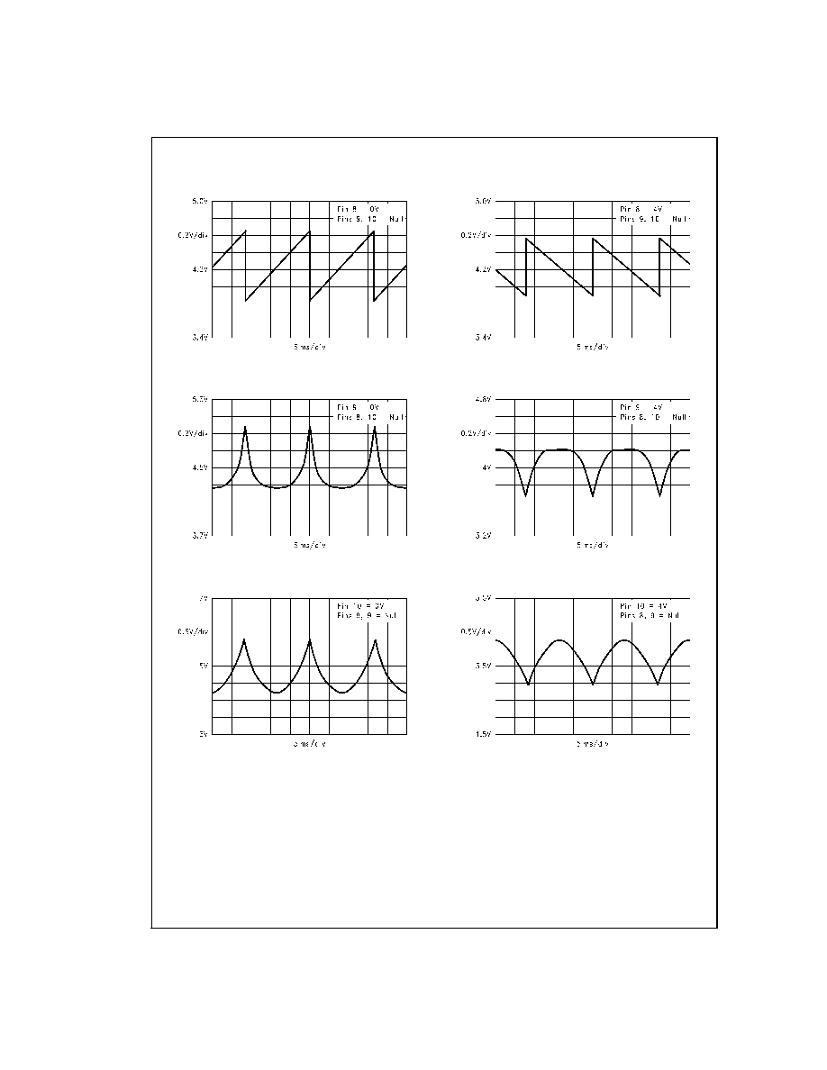
Typical Performance Characteristics
(Continued)
E-W Out (Pin 11)
DS012894-3
E-W Out (Pin 11)
DS012894-4
E-W Out (Pin 11)
DS012894-5
E-W Out (Pin 11)
DS012894-6
E-W Out (Pin 11)
DS012894-7
E-W Out (Pin 11)
DS012894-8
www.national.com
4
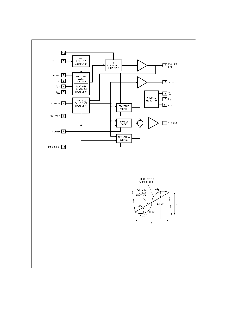
Block Diagram
Functional Description
The LM1296 outputs a sawtooth and a variable DC voltage
for the vertical deflection amplifier. It also provides the hori-
zontal deflection output circuit with a waveform for Trap-
ezoid, Pincushion and Corner correction.
Referring to
Figure 3, pin 7 (V SYNC) goes to the Sync Po-
larity Correction Block that accepts either positive-going or
negative-going sync signals. The polarity-corrected sync is
sent to the Injection-Locked Oscillator so that the sawtooth
generated is synchronized with the vertical sync. With no
sync signal AC-coupled to pin 7, the oscillator free runs at
typically 40 Hz.
There are three capacitors and one control pin connected to
the Sawtooth Waveform Generation Block. C
OSC
is the tim-
ing capacitor for the Injection-Locked Oscillator. C
F
is the fil-
ter capacitor for an internal circuit that detects the existence
of vertical sync and prevents the Injection-Locked Oscillator
from locking at twice the vertical sync frequency. C
ALC
is for
the automatic level control (ALC) circuit. The ALC circuit
maintains the sawtooth output amplitude, which is set by the
DC voltage at pin 2 (HEIGHT), regardless of the vertical sync
frequency. Since the output sawtooth goes to the geometry
correction circuit as well, the correction waveform generated
tracks the sawtooth amplitude, i.e., the height of the CRT
raster.
The S Correction block shapes the linear sawtooth into an
S-shape sawtooth. Pin 15 (SAWTOOTH OUT) outputs the
buffered S-shape sawtooth. The amount of S correction is
controlled by the DC voltage at pin 16 (S).
Referring to
Figure 4, the extent of S correction is defined by
the following equation.
k
S
= (
A
1
+
A
2
)/2A x 100%
The LM1296 is designed to drive an external vertical deflec-
tion amplifier that is operating with positive and negative
power supplies. The LM1296 outputs an S-corrected saw-
tooth with a DC level that is typical 3.85V. Pin 13 (DC OUT)
provides a DC voltage of 3.85V
±
200 mV. By applying a DC
control voltage to pin 1 (POSITION), the output voltage at pin
13 can be varied. This sets the output DC current from the
vertical deflection amplifier, which in turn sets the raster ver-
tical position.
DS012894-9
FIGURE 3.
DS012894-10
FIGURE 4.
5
www.national.com