TL H 11879
LM12434LM12
L
438
12-Bit
a
Sign
Data
Acquisition
System
with
Serial
IO
and
Self-Calibration
July 1995
LM12434 LM12 L 438 12-Bit
a
Sign Data Acquisition
System with Serial I O and Self-Calibration
General Description
The LM12434 and LM12 L 438 are highly integrated Data
Acquisition Systems Operating on 3V to 5V they combine a
fully-differential self-calibrating (correcting linearity and zero
errors) 13-bit (12-bit
a
sign) analog-to-digital converter
(ADC) and sample-and-hold (S H) with extensive analog
and digital functionality Up to 32 consecutive conversions
using two's complement format can be stored in an internal
32-word (16-bit wide) FIFO data buffer An internal 8-word
instruction RAM can store the conversion sequence for up
to eight acquisitions through the LM12 L 438's eight-input
multiplexer The LM12434 has a four-channel multiplexer a
differential multiplexer output and a differential S H input
The LM12434 and LM12 L 438 can also operate with 8-bit
a
sign resolution and in a supervisory ``watchdog'' mode
that compares an input signal against two programmable
limits
Acquisition times and conversion rates are programmable
through the use of internal clock-driven timers The differen-
tial reference voltage inputs can be externally driven for ab-
solute or ratiometric operation
All registers RAM and FIFO are directly accessible through
the high speed and flexible serial I O interface bus The
serial interface bus is user selectable to interface with the
following protocols with zero glue logic
MICROWIRE
PLUS
TM
Motorola's SPI QSPI Hitachi's SCI 8051 Family's
Serial Port (Mode 0) I
2
C and the TMS320 Family's Serial
Port
An evaluation kit for demonstrating the LM12434 and
LM12 L 438 is available
TRI-STATE
is a registered trademark of National Semiconductor Corporation
MICROWIRE PLUS
TM
is a trademark of National Semiconductor Corporation
Windows
is a registered trademark of Microsoft Corporation
Key Specifications
f
CLK
e
8 MHz L f
CLK
e
6 MHz
Y
Resolution
12-bit
a
sign or 8-bit
a
sign
Y
13-bit conversion time
5 5 ms 7 3 ms (max)
Y
9-bit conversion time
2 6 ms 3 5 ms (max)
Y
13-bit Through-put rate
140k samples s 105k sample s (min)
Y
Comparison time (``watchdog'' mode)
1 4 ms 1 8 ms (max)
Y
Serial Clock
10 MHz 6 MHz (max)
Y
Integral Linearity Error
g
1 LSB (max)
Y
V
IN
range
GND to V
A
a
Y
Power dissipation
45 mW 20 mW (max)
Y
Stand-by mode
power dissipation
25 mW 16 5 mW (typ)
Y
Supply voltage LM12L438
3 3V
g
10%
LM12434 8
5V
g
10%
Features
Y
Three operating modes 12-bit
a
sign 8-bit
a
sign
and ``watchdog'' comparison mode
Y
Single-ended or differential inputs
Y
Built-in Sample-and-Hold
Y
Instruction RAM and event sequencer
Y
8-channel (LM12 L 438) or 4-channel (LM12434)
multiplexer
Y
32-word conversion FIFO
Y
Programmable acquisition times and conversion rates
Y
Self-calibration and diagnostic mode
Y
Power down output for system power management
Y
Read while convert capability for maximum through-put
rate
Applications
Y
Data Logging
Y
Portable Instrumentation
Y
Process Control
Y
Energy Management
Y
Robotics
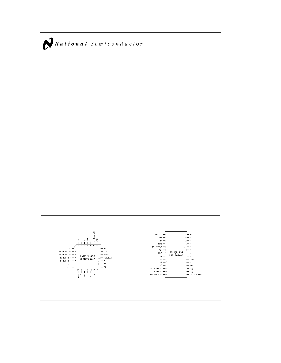
Connection Diagrams
28-Pin PLCC Package
TL H 11879 � 1
Pin names in ( ) apply to the LM12434
Order Number LM12434CIV LM12438CIV or
LM12L438CIV
See NS Package Number V28A
28-Pin Wide Body SO Package
TL H 11879 � 2
Order Number LM12434CIWM LM12438CIWM or
LM12L438CIWM
See NS Package Number M28B
C1995 National Semiconductor Corporation
RRD-B30M85 Printed in U S A

Table of Contents
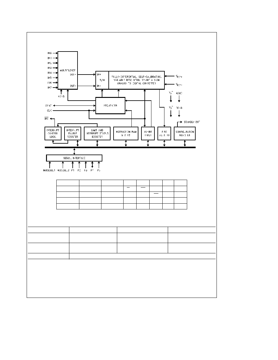
1 0 FUNCTIONAL DIAGRAMS
3
2 0 ELECTRICAL SPECIFICATIONS
5
2 1 Ratings
5
2 1 1 Absolute Maximum Ratings
5
2 1 2 Operating Ratings
5
2 2 Performance Characteristics
5
2 2 1 Converter Static Characteristics
5
2 2 2 Converter Dynamic Characteristics
6
2 2 3 DC Characteristics
8
2 2 4 Digital DC Characteristics
9
2 3 Digital Switching Characteristics
10
2 3 1 Standard Interface Mode
10
2 3 2 8051 Interface Mode
11
2 3 3 TMS320 Interface Mode
12
2 3 4 I
2
C Bus Interface
13
2 4 Notes on Specifications
14
3 0 ELECTRICAL CHARACTERISTICS
15
4 0 TYPICAL PERFORMANCE CHARACTERISTICS
19
5 0 PIN DESCRIPTIONS
23
6 0 OPERATIONAL INFORMATION
27
6 1 Functional Description
27
6 2 Internal User-Accessible Registers
31
6 2 1 Instruction RAM
31
6 2 2 Configuration Register
38
6 2 3 Interrupts
38
6 2 4 Interrupt Enable Register
39
6 2 5 Interrupt Status Register
39
6 2 6 Limit Status Register
40
6 2 7 Timer
40
6 2 8 FIFO
40
6 3 Instruction Sequencer
41
7 0 DIGITAL INTERFACE
43
7 1 Standard Interface Mode
43
7 1 1 Examples of Interfacing to the HPC 46XXX's
MICROWIRE PLUS
TM
and 68HC11's SPI
50
7 2 8051 Interface Mode
59
7 2 1 Example of Interfacing to the 8051
62
7 3 TMS320 Interface Mode
66
7 3 1 Example of Interfacing to the TMS320C3x
69
7 4 I
2
C Bus Interface
74
7 4 1 Example of Interfacing to an I
2
C Controller
76
8 0 ANALOG CONSIDERATIONS
77
8 1 Reference Voltage
77
8 2 Input Range
77
8 3 Input Current
77
8 4 Input Source Resistance
77
8 5 Input Bypass Capacitance
77
8 6 Input Noise
77
8 7 Power Supply Consideration
77
8 8 PC Board Layout and Grounding Consideration
78
2

1 0 Functional Diagrams
LM12434
TL H 11879 � 3
INTERFACE
MODESEL1
MODESEL2
P1
P2
P3
P4
P5
Standard
0
1
R F
CS
DI
DO
SCLK
8051
0
0
1
1
CS
RXD
TXD
I
2
C
1
0
SAD0
SAD1
SAD2
SDA
SCL
TMS320
1
1
FSR
FSX
DX
DR
SCLK
Internal pull-up
Ordering Information (LM12434)
Part Number
Package Type
NSC Package Number
Temperature Range
LM12434CIV
28-Pin PLCC
V28A
b
40 C to
a
85 C
LM12434CIWM
28-Pin Wide Body SO
M28B
b
40 C to
a
85 C
3
1 0 Functional Diagrams
(Continued)
LM12 L 438
TL H 11879 � 4
INTERFACE
MODESEL1
MODESEL2
P1
P2
P3
P4
P5
Standard
0
1
R F
CS
DI
DO
SCLK
8051
0
0
1
1
CS
RXD
TXD
I
2
C
1
0
SAD0
SAD1
SAD2
SDA
SCL
TMS320
1
1
FSR
FSX
DX
DR
SCLK
Internal pull-up
Ordering Information (LM12 L 438)
Part Number
Package Type
NSC Package Number
Temperature Range
LM12438CIV
28-Pin PLCC
V28A
b
40 C to
a
85 C
LM12L438CIV
LM12438CIWM
28-Pin Wide Body SO
M28B
b
40 C to
a
85 C
LM12L438CIWM
LM12438 Eval
Evaluation Board and Windows based software
4
2 0 Electrical Specifications
2 1 RATINGS
2 1 1 Absolute Maximum Ratings
(Notes 1
2)
If Military Aerospace specified devices are required
please contact the National Semiconductor Sales
Office Distributors for availability and specifications
Supply Voltage (V
A
a
and V
D
a
)
6 0V
Voltage at Input and Output Pins
except IN0 � IN3 (LM12434)
b
0 3V to V
a
a
0 3V
and IN0 � IN7 (LM12 L 438)
Voltage at Analog Inputs IN0 � IN3 (LM12434)
and IN0 � IN7 (LM12 L 438)
GND
b
5V to V
a
a
5V
l
V
A
a
b
V
D
a
l
300 mV
l
AGND
b
DGND
l
300 mV
Input Current at Any Pin (Note 3)
g
5 mA
Package Input Current (Note 3)
g
20 mA
Power Dissipation (T
A
e
25 C) (Note 4)
V Package
WM Package
Storage Temperature
b
65 C to
a
150 C
Soldering Information Lead Temperature (Note 19)
V Package Vapor Phase (60 seconds)
Infrared (15 seconds)
WM Package Vapor Phase (60 seconds)
Infrared (15 seconds)
ESD Susceptibility (Note 5)
1 5 kV
2 1 2 Operating Ratings
(Notes 1
2)
Temperature Range
(T
min
s
T
A
s
T
max
)
LM12434CIV LM12 L 438CIV
b
40 C
s
T
A
s
85 C
LM12434CIWM LM12 L 438CIWM
b
40 C
s
T
A
s
85 C
Supply Voltage
V
A
a
V
D
a
3 0V to 5 5V
l
V
A
a
b
V
D
a
l
s
100 mV
l
AGDND
b
DGND
l
s
100 mV
Analog Inputs Range
GND
s
V
INa
s
V
A
a
V
REFa
Input Voltage
1V
s
V
REFa
s
V
A
a
V
REFb
Input Voltage
0V
s
V
REFb
s
V
REFa
b
1V
V
REFa
b
V
REFb
1V
s
V
REF
s
V
A
a
V
REF
Common Mode
Range (Note 16)
0 1 V
A
a s
V
REFCM
s
0 6 V
A
a
2 2 PERFORMANCE CHARACTERISTICS
All specifications apply to the LM12434 LM12438 and LM12L438 unless otherwise
noted Specifications in braces
apply only to the LM12L438
2 2 1 Converter Static Characteristics
The following specifications apply to the LM12434 and LM12 L 438 for V
A
a
e
V
D
a
e
5V 3 3V
AGND
e
DGND
e
0V V
REFa
e
4 096V 2 5V
V
REFb
e
0V 12-bit
a
sign conversion mode f
CLK
e
8 0 MHz
6 MHz
R
S
e
25X source impedance for V
REFa
and V
REFb
s
25X fully-differential input with fixed 2 048V
1 25V common-mode voltage and minimum acquisition time unless otherwise specified Boldface limits apply for T
A
e
T
J
e
T
MIN
to T
MAX
all other limits T
A
e
T
J
e
25 C (Notes 6 7 8 and 9)
Symbol
Parameter
Conditions
Typical
Limits
Units
(Note 10)
(Note 11)
(Limit)
ILE
Positive and Negative Integral
After Auto-Cal (Notes 12 17)
g
0 35
g
1
LSB (max)
Linearity Error
TUE
Total Unadjusted Error
After Auto-Cal (Note 12)
g
1
LSB
Resolution with No Missing Codes
After Auto-Cal (Note 12)
13
Bits
DNL
Differential Non-Linearity
After Auto-Cal
g
0 2
g
1
LSB (max)
Zero Error
After Auto-Cal (Notes 13 17)
g
0 2
g
1
LSB (max)
Positive Full-Scale Error
After Auto-Cal (Notes 12 17)
g
0 2
g
2
LSB (max)
Negative Full-Scale Error
After Auto-Cal (Notes 12 17)
g
0 2
g
2
LSB (max)
DC Common Mode Error
(Note 14)
g
2
g
3 5
LSB (max)
g
4 0
ILE
8-Bit
a
Sign and ``Watchdog''
(Note 12)
Mode Positive and Negative
g
0 15
g
1 2
LSB (max)
Integral Linearity Error
TUE
8-Bit
a
Sign and ``Watchdog'' Mode
After Auto-Zero
g
1 2
g
1 2
LSB (max)
Total Unadjusted Error
8-Bit
a
Sign and ``Watchdog'' Mode
9
Bits (max)
Resolution with No Missing Codes
5