LM13600
Dual Operational Transconductance Amplifiers with
Linearizing Diodes and Buffers
General Description
The LM13600 series consists of two current controlled
transconductance amplifiers each with differential inputs and
a push-pull output. The two amplifiers share common sup-
plies but otherwise operate independently. Linearizing di-
odes are provided at the inputs to reduce distortion and allow
higher input levels. The result is a 10 dB signal-to-noise im-
provement referenced to 0.5 percent THD. Controlled im-
pedance buffers which are especially designed to comple-
ment the dynamic range of the amplifiers are provided.
Features
n
g
m
adjustable over 6 decades
n
Excellent g
m
linearity
n
Excellent matching between amplifiers
n
Linearizing diodes
n
Controlled impedance buffers
n
High output signal-to-noise ratio
Applications
n
Current-controlled amplifiers
n
Current-controlled impedances
n
Current-controlled filters
n
Current-controlled oscillators
n
Multiplexers
n
Timers
n
Sample and hold circuits
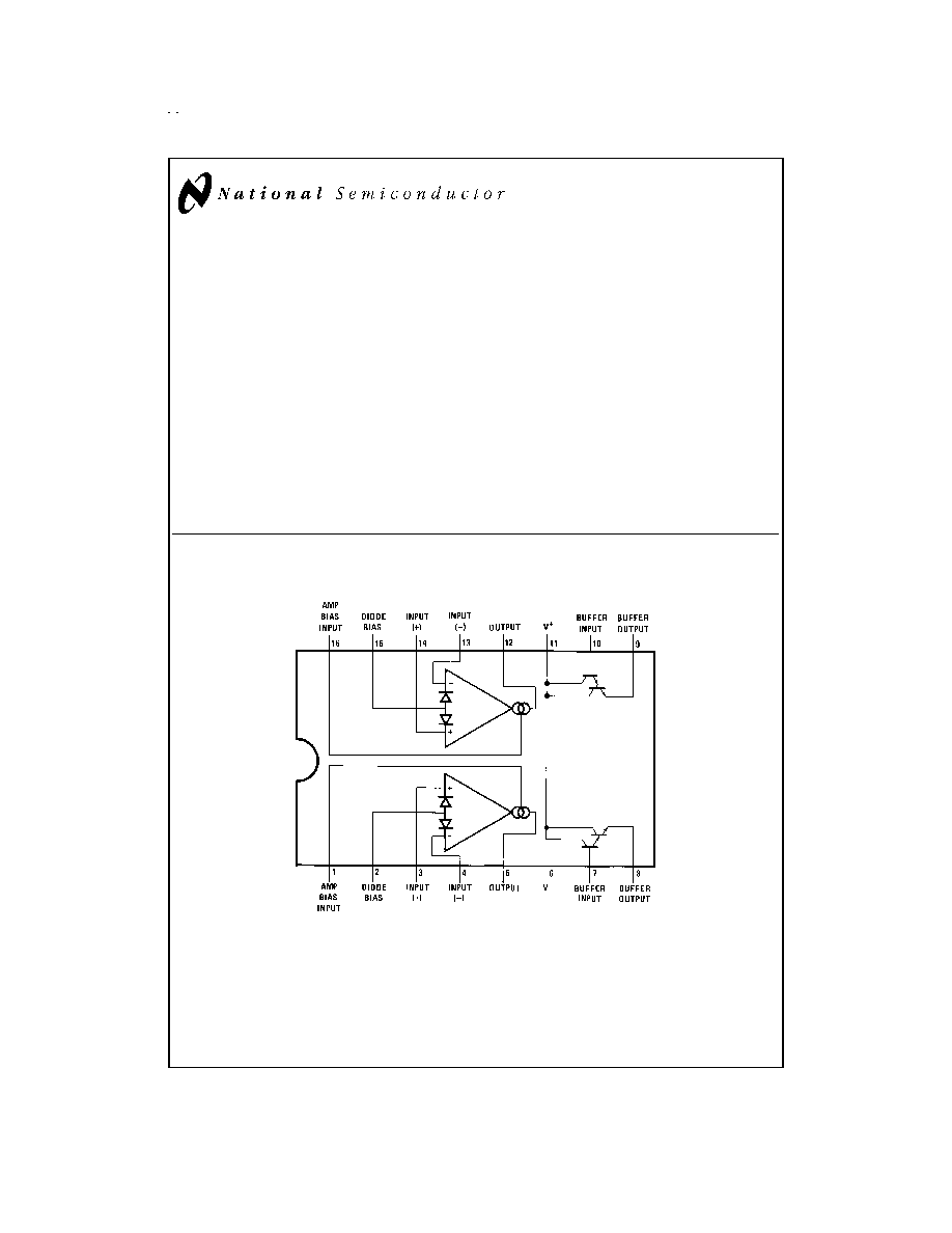
Connection Diagram
Dual-In-Line and Small Outline Packages
DS007980-2
Top View
Order Number LM13600M, LM13600N or LM13600AN
See NS Package Number M16A or N16A
May 1998
LM13600
Dual
Operational
T
ransconductance
Amplifiers
with
Linearizing
Diodes
and
Buffers
� 1999 National Semiconductor Corporation
DS007980
www.national.com
Absolute Maximum Ratings
(Note 1)
If Military/Aerospace specified devices are required,
please contact the National Semiconductor Sales Office/
Distributors for availability and specifications.
Supply Voltage (Note 2)
LM13600
36 V
DC
or
�
18V
LM13600A
44 V
DC
or
�
22V
Power Dissipation (Note 3) T
A
= 25�C
570 mW
Differential Input Voltage
�
5V
Diode Bias Current (I
D
)
2 mA
Amplifier Bias Current (I
ABC
)
2 mA
Output Short Circuit Duration
Continuous
Buffer Output Current (Note 4)
20 mA
Operating Temperature Range
0�C to +70�C
DC Input Voltage
+V
S
to -V
S
Storage Temperature Range
-65�C to +150�C
Soldering Information
Dual-In-Line Package
Soldering (10 seconds)
260�C
Small Outline Package
Vapor Phase (60 seconds)
215�C
Infrared (15 seconds)
220�C
See AN-450 "Surface Mounting Methods and Their Effect
on Product Reliability" for other methods of soldering
surface mount devices.
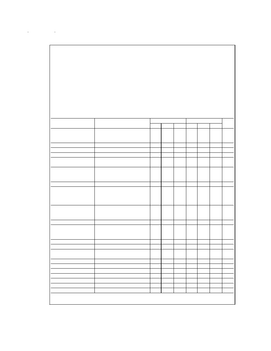
Electrical Characteristics
(Note 5)
Parameter
Conditions
LM13600
LM13600A
Units
Min
Typ
Max
Min
Typ
Max
Input Offset Voltage (V
OS
)
0.4
4
0.4
1
mV
Over Specified Temperature Range
2
mV
I
ABC
= 5 �A
0.3
4
0.3
1
mV
V
OS
Including Diodes
Diode Bias Current (I
D
) = 500 �A
0.5
5
0.5
2
mV
Input Offset Change
5 �A
I
ABC
500 �A
0.1
3
0.1
1
mV
Input Offset Current
0.1
0.6
0.1
0.6
�A
Input Bias Current
0.4
5
0.4
5
�A
Over Specified Temperature Range
1
8
1
7
�A
Forward
Transconductance (g
m
)
6700
9600
13000
7700
9600
12000
�mho
Over Specified Temperature Range
5400
4000
�mho
g
m
Tracking
0.3
0.3
dB
Peak Output Current
R
L
= 0, I
ABC
= 5 �A
5
3
5
7
�A
R
L
= 0, I
ABC
= 500 �A
350
500
650
350
500
650
�A
R
L
= 0, Over Specified Temp
Range
300
300
�A
Peak Output Voltage
Positive
R
L
=
, 5 �A
I
ABC
500 �A
+12
+14.2
+12
+14.2
V
Negative
R
L
=
, 5 �A
I
ABC
500 �A
-12
-14.4
-12
-14.4
V
Supply Current
I
ABC
= 500 �A, Both Channels
2.6
2.6
mA
V
OS
Sensitivity
Positive
V
OS
/
V+
20
150
20
150
�V/V
Negative
V
OS
/
V-
20
150
20
150
�V/V
CMRR
80
110
80
110
dB
Common Mode Range
�
12
�
13.5
�
12
�
13.5
V
Crosstalk
Referred to Input (Note 6)
100
100
dB
20 Hz
<
f
<
20 kHz
Differential Input Current
I
ABC
= 0, Input =
�
4V
0.02
100
0.02
10
nA
Leakage Current
I
ABC
= 0 (Refer to Test Circuit)
0.2
100
0.2
5
nA
Input Resistance
10
26
10
26
k
Open Loop Bandwidth
2
2
MHz
Slew Rate
Unity Gain Compensated
50
50
V/�s
Buffer Input Current
(Note 6), Except I
ABC
= 0 �A
0.2
0.4
0.2
0.4
�A
Peak Buffer Output Voltage
(Note 6)
10
10
V
www.national.com
2
Electrical Characteristics
(Note 5) (Continued)
Note 1: "Absolute Maximum Ratings" indicate limits beyond which damage to the device may occur. Operating Ratings indicate conditions for which the device is
functional, but do not guarantee specific performance limits.
Note 2: For selections to a supply voltage above
�
22V, contact factory.
Note 3: For operating at high temperatures, the device must be derated based on a 150�C maximum junction temperature and a thermal resistance of 175�C/W
which applies for the device soldered in a printed circuit board, operating in still air.
Note 4: Buffer output current should be limited so as to not exceed package dissipation.
Note 5: These specifications apply for V
S
=
�
15V, T
A
= 25�C, amplifier bias current (I
ABC
) = 500 �A, pins 2 and 15 open unless otherwise specified. The inputs to
the buffers are grounded and outputs are open.
Note 6: These specifications apply for V
S
=
�
15V, I
ABC
= 500 �A, R
OUT
= 5 k
connected from the buffer output to -V
S
and the input of the buffer is connected
to the transconductance amplifier output.
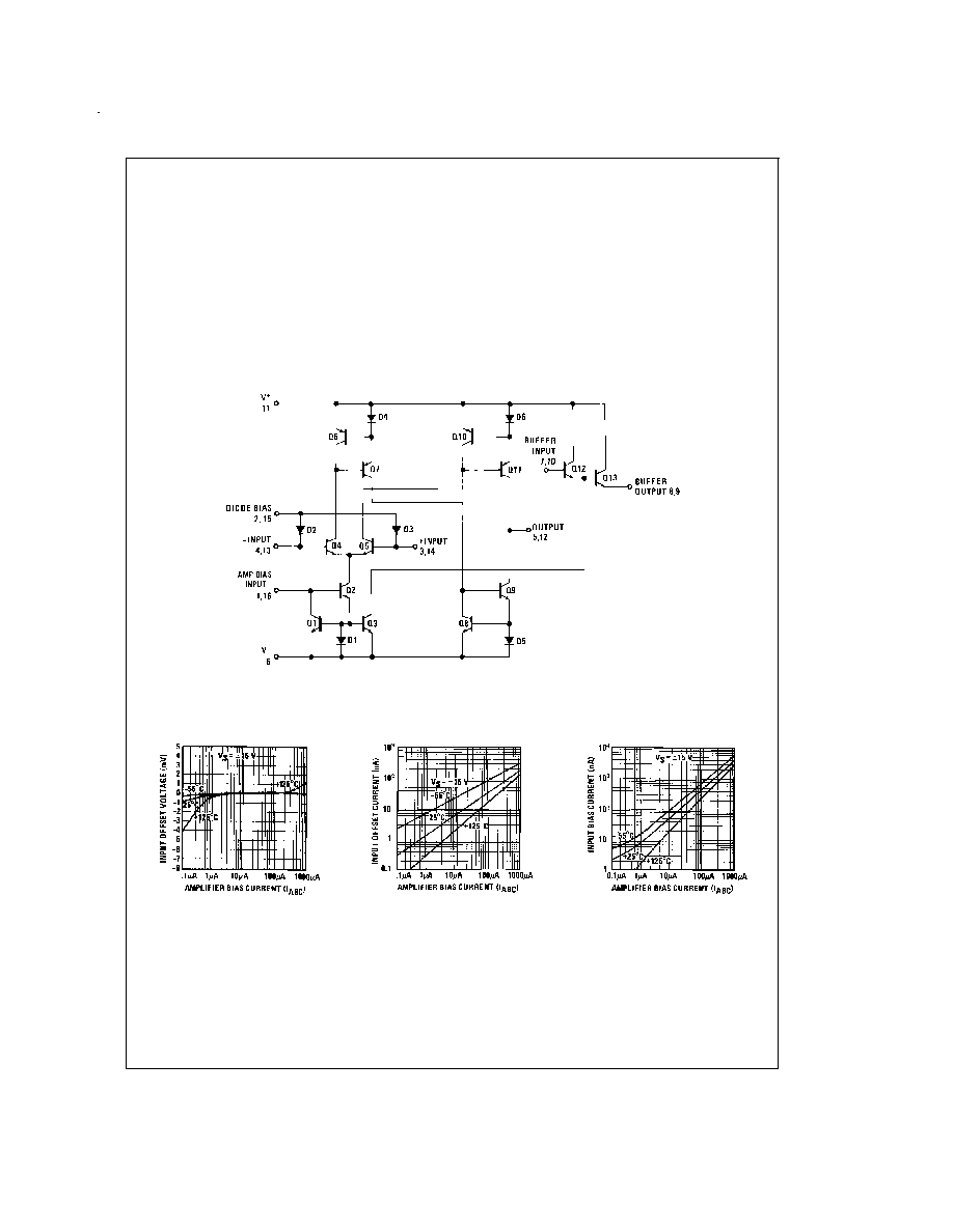
Schematic Diagram
Typical Performance Characteristics
One Operational Transconductance Amplifier
DS007980-1
Input Offset Voltage
DS007980-39
Input Offset Current
DS007980-40
Input Bias Current
DS007980-41
www.national.com
3
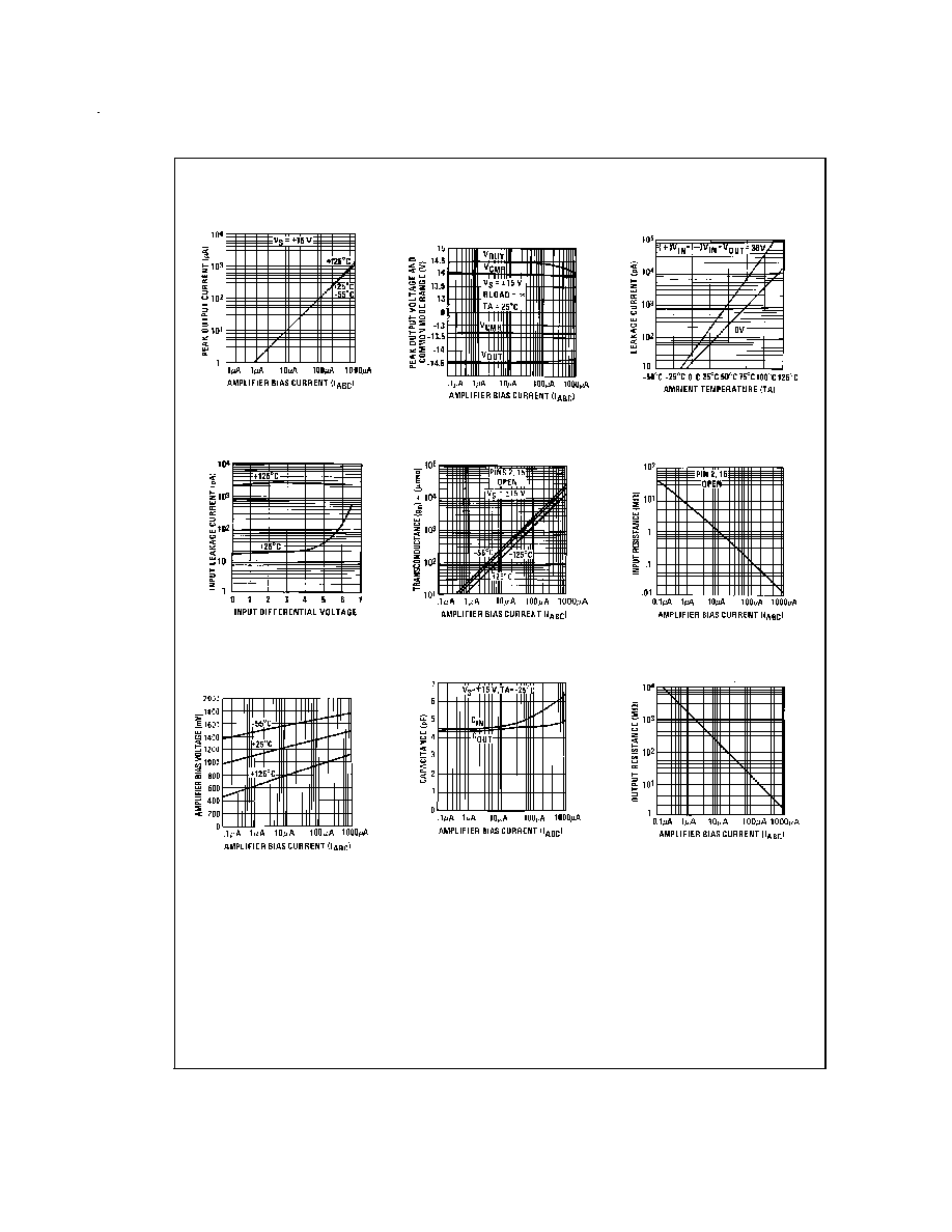
Typical Performance Characteristics
(Continued)
Peak Output Current
DS007980-42
Peak Output Voltage and
Common Mode Range
DS007980-43
Leakage Current
DS007980-44
Input Leakage
DS007980-45
Transconductance
DS007980-46
Input Resistance
DS007980-47
Amplifier Bias Voltage vs
Amplifier Bias Current
DS007980-48
Input and Output Capacitance
DS007980-49
Output Resistance
DS007980-50
www.national.com
4
Typical Performance Characteristics
(Continued)
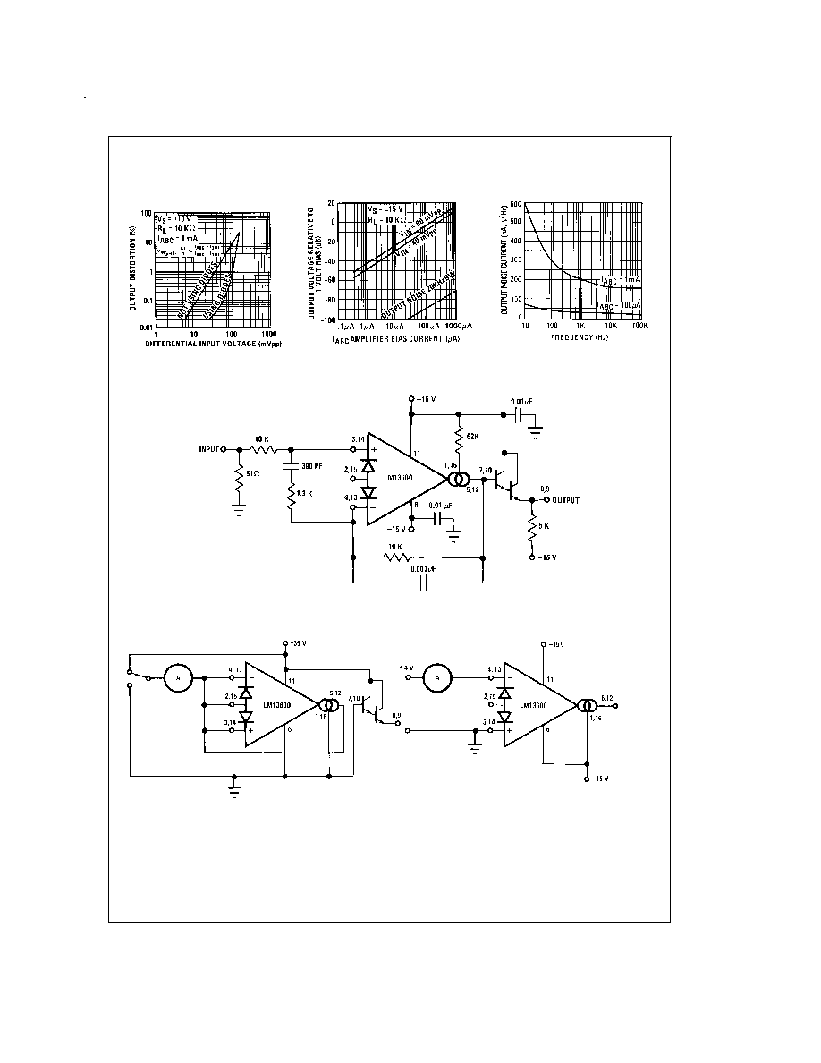
Distortion vs Differential
Input Voltage
DS007980-51
Voltage vs Amplifier Bias Current
DS007980-52
Output Noise vs Frequency
DS007980-53
Unity Gain Follower
DS007980-5
Leakage Current Test Circuit
DS007980-6
Differential Input Current Test Circuit
DS007980-7
www.national.com
5