LM340/LM78XX Series
3-Terminal Positive Regulators
General Description
The
LM140/LM340A/LM340/LM78XXC
monolithic
3-terminal positive voltage regulators employ internal
current-limiting, thermal shutdown and safe-area compensa-
tion, making them essentially indestructible. If adequate heat
sinking is provided, they can deliver over 1.0A output cur-
rent. They are intended as fixed voltage regulators in a wide
range of applications including local (on-card) regulation for
elimination of noise and distribution problems associated
with single-point regulation. In addition to use as fixed volt-
age regulators, these devices can be used with external
components to obtain adjustable output voltages and cur-
rents.
Considerable effort was expended to make the entire series
of regulators easy to use and minimize the number of exter-
nal components. It is not necessary to bypass the output,
although this does improve transient response. Input by-
passing is needed only if the regulator is located far from the
filter capacitor of the power supply.
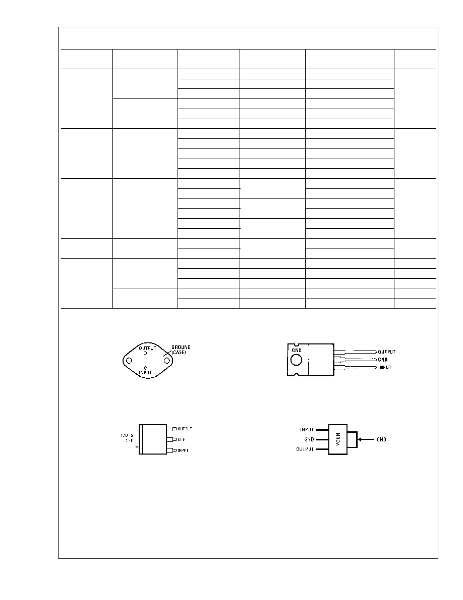
The 5V, 12V, and 15V regulator options are available in the
steel TO-3 power package. The LM340A/LM340/LM78XXC
series is available in the TO-220 plastic power package, and
the LM340-5.0 is available in the SOT-223 package, as well
as the LM340-5.0 and LM340-12 in the surface-mount TO-
263 package.
Features
n
Complete specifications at 1A load
n
Output voltage tolerances of
±
2% at T
j
= 25∞C and
±
4%
over the temperature range (LM340A)
n
Line regulation of 0.01% of V
OUT
/V of
V
IN
at 1A load
(LM340A)
n
Load regulation of 0.3% of V
OUT
/A (LM340A)
n
Internal thermal overload protection
n
Internal short-circuit current limit
n
Output transistor safe area protection
n
P
+
Product Enhancement tested
Typical Applications
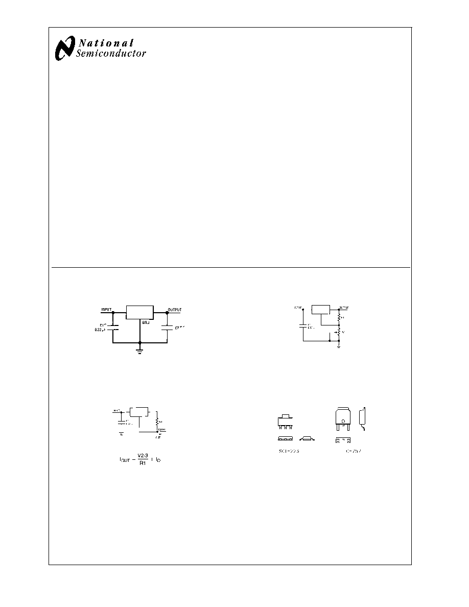
Fixed Output Regulator
Adjustable Output Regulator
00778101
*Required if the regulator is located far from the power supply filter.
**Although no output capacitor is needed for stability, it does help transient
response. (If needed, use 0.1 µF, ceramic disc).
00778102
V
OUT
= 5V + (5V/R1 + I
Q
) R2 5V/R1
>
3 I
Q
,
load regulation (L
r
)
[(R1 + R2)/R1] (L
r
of LM340-5).
Current Regulator
Comparison between SOT-223 and D-Pak (TO-252)
Packages
00778103
I
Q
= 1.3 mA over line and load changes.
00778138
Scale 1:1
November 2004
LM340/LM78XX
Series
3-T
erminal
Positive
Regulators
© 2004 National Semiconductor Corporation
DS007781
www.national.com
Absolute Maximum Ratings
(Note 1)
If Military/Aerospace specified devices are required,
please contact the National Semiconductor Sales Office/
Distributors for availability and specifications.
(Note 5)
DC Input Voltage
35V
Internal Power Dissipation (Note 2)
Internally Limited
Maximum Junction Temperature
150∞C
Storage Temperature Range
-65∞C to +150∞C
Lead Temperature (Soldering, 10 sec.)
TO-3 Package (K)
300∞C
TO-220 Package (T), TO-263
Package (S)
230∞C
ESD Susceptibility (Note 3)
2 kV
Operating Conditions
(Note 1)
Temperature Range (T
A
) (Note 2)
LM140
-55∞C to +125∞C
LM340A, LM340
0∞C to +125∞C
LM7808C
0∞C to +125∞C
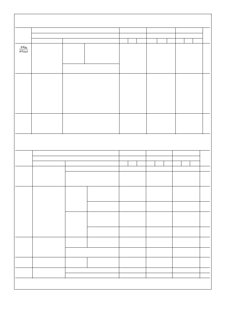
LM340A Electrical Characteristics
I
OUT
= 1A, 0∞C
T
J
+ 125∞C (LM340A) unless otherwise specified (Note 4)
Output Voltage
5V
12V
15V
Symbol
Input Voltage (unless otherwise noted)
10V
19V
23V
Units
Parameter
Conditions
Min
Typ Max
Min
Typ Max
Min
Typ Max
V
O
Output Voltage
T
J
= 25∞C
4.9
5
5.1
11.75
12 12.25
14.7
15
15.3
V
P
D
15W, 5 mA I
O
1A
4.8
5.2
11.5
12.5
14.4
15.6
V
V
MIN
V
IN
V
MAX
(7.5
V
IN
20) (14.8 V
IN
27) (17.9 V
IN
30)
V
V
O
Line Regulation
I
O
= 500 mA
10
18
22
mV
V
IN
(7.5
V
IN
20) (14.8 V
IN
27) (17.9 V
IN
30)
V
T
J
= 25∞C
3
10
4
18
4
22
mV
V
IN
(7.5
V
IN
20) (14.5 V
IN
27) (17.5 V
IN
30)
V
T
J
= 25∞C
4
9
10
mV
Over Temperature
12
30
30
mV
V
IN
(8
V
IN
12)
(16
V
IN
22)
(20
V
IN
26)
V
V
O
Load Regulation
T
J
= 25∞C
5 mA
I
O
1.5A
10
25
12
32
12
35
mV
250 mA
I
O
750
mA
15
19
21
mV
Over Temperature,
25
60
75
mV
5 mA
I
O
1A
I
Q
Quiescent
Current
T
J
= 25∞C
6
6
6
mA
Over Temperature
6.5
6.5
6.5
mA
I
Q
Quiescent
Current
5 mA
I
O
1A
0.5
0.5
0.5
mA
Change
T
J
= 25∞C, I
O
= 1A
0.8
0.8
0.8
mA
V
MIN
V
IN
V
MAX
(7.5
V
IN
20) (14.8 V
IN
27) (17.9 V
IN
30)
V
I
O
= 500 mA
0.8
0.8
0.8
mA
V
MIN
V
IN
V
MAX
(8
V
IN
25)
(15
V
IN
30)
(17.9
V
IN
30)
V
V
N
Output Noise
Voltage
T
A
= 25∞C, 10 Hz
f 100 kHz
40
75
90
µV
Ripple Rejection
T
J
= 25∞C, f = 120 Hz, I
O
= 1A
68
80
61
72
60
70
dB
or f = 120 Hz, I
O
= 500 mA,
68
61
60
dB
Over Temperature,
V
MIN
V
IN
V
MAX
(8
V
IN
18)
(15
V
IN
25)
(18.5
V
IN
28.5)
V
R
O
Dropout Voltage
T
J
= 25∞C, I
O
= 1A
2.0
2.0
2.0
V
Output
Resistance
f = 1 kHz
8
18
19
m
Short-Circuit
Current
T
J
= 25∞C
2.1
1.5
1.2
A
LM340/LM78XX
www.national.com
3
LM340A Electrical Characteristics
(Continued)
I
OUT
= 1A, 0∞C
T
J
+ 125∞C (LM340A) unless otherwise specified (Note 4)
Output Voltage
5V
12V
15V
Symbol
Input Voltage (unless otherwise noted)
10V
19V
23V
Units
Parameter
Conditions
Min
Typ Max
Min
Typ Max
Min
Typ Max
Peak Output
Current
T
J
= 25∞C
2.4
2.4
2.4
A
Average TC of
V
O
Min, T
J
= 0∞C, I
O
= 5 mA
-0.6
-1.5
-1.8
mV/∞C
V
IN
Input Voltage
T
J
= 25∞C
Required to
Maintain
7.5
14.5
17.5
V
Line Regulation
LM140 Electrical Characteristics
(Note 4)
-55∞C
T
J
+150∞C unless otherwise specified
Output Voltage
5V
12V
15V
Symbol
Input Voltage (unless otherwise noted)
10V
19V
23V
Units
Parameter
Conditions
Min Typ
Max
Min
Typ
Max Min Typ
Max
V
O
Output Voltage
T
J
= 25∞C, 5 mA
I
O
1A
4.8
5
5.2
11.5
12
12.5 14.4
15
15.6
V
P
D
15W, 5 mA I
O
1A
4.75
5.25
11.4
12.6 14.25
15.75
V
V
MIN
V
IN
V
MAX
(8
V
IN
20)
(15.5
V
IN
27)
(18.5
V
IN
30)
V
V
O
Line Regulation
I
O
= 500 mA
T
J
= 25∞C
3
50
4
120
4
150 mV
V
IN
(7
V
IN
25)
(14.5
V
IN
30)
(17.5
V
IN
30)
V
-55∞C
T
J
+150∞C
50
120
150 mV
V
IN
(8
V
IN
20)
(15
V
IN
27)
(18.5
V
IN
30)
V
I
O
1A
T
J
= 25∞C
50
120
150 mV
V
IN
(7.5
V
IN
20) (14.6 V
IN
27)
(17.7
V
IN
30)
V
-55∞C
T
J
+150∞C
25
60
75
mV
V
IN
(8
V
IN
12)
(16
V
IN
22)
(20
V
IN
26)
V
V
O
Load Regulation
T
J
= 25∞C
5 mA
I
O
1.5A
10
50
12
120
12
150 mV
250 mA
I
P
750
mA
25
60
75
mV
-55∞C
T
J
+150∞C,
50
120
150 mV
5 mA
I
O
1A
I
Q
Quiescent Current
I
O
1A
T
J
= 25∞C
6
6
6
mA
-55∞C
T
J
+150∞C
7
7
7
mA
I
Q
Quiescent Current
5 mA
I
O
1A
0.5
0.5
0.5
mA
Change
T
J
= 25∞C, I
O
1A
0.8
0.8
0.8
mA
V
MIN
V
IN
V
MAX
(8
V
IN
20)
(15
V
IN
27)
(18.5
V
IN
30)
V
I
O
= 500 mA, -55∞C
T
J
+150∞C
0.8
0.8
0.8
mA
V
MIN
V
IN
V
MAX
(8
V
IN
25)
(15
V
IN
30)
(18.5
V
IN
30)
V
V
N
Output Noise
Voltage
T
A
= 25∞C, 10 Hz
f 100 kHz
40
75
90
µV
LM340/LM78XX
www.national.com
4
LM140 Electrical Characteristics
(Note 4) (Continued)
-55∞C
T
J
+150∞C unless otherwise specified
Output Voltage
5V
12V
15V
Symbol
Input Voltage (unless otherwise noted)
10V
19V
23V
Units
Parameter
Conditions
Min Typ
Max
Min
Typ
Max Min Typ
Max
Ripple Rejection
I
O
1A, T
J
= 25∞C
or
68
80
61
72
60
70
dB
f = 120 Hz
I
O
500 mA,
68
61
60
dB
-55∞C
T
J
+150∞C
V
MIN
V
IN
V
MAX
(8
V
IN
18)
(15
V
IN
25)
(18.5
V
IN
28.5)
V
R
O
Dropout Voltage
T
J
= 25∞C, I
O
= 1A
2.0
2.0
2.0
V
Output Resistance
f = 1 kHz
8
18
19
m
Short-Circuit
Current
T
J
= 25∞C
2.1
1.5
1.2
A
Peak Output
Current
T
J
= 25∞C
2.4
2.4
2.4
A
Average TC of
V
OUT
0∞C
T
J
+150∞C, I
O
= 5 mA
-0.6
-1.5
-1.8
mV/∞C
V
IN
Input Voltage
T
J
= 25∞C, I
O
1A
Required to
Maintain
7.5
14.6
17.7
V
Line Regulation
LM340 Electrical Characteristics
(Note 4)
0∞C
T
J
+125∞C unless otherwise specified
Output Voltage
5V
12V
15V
Symbol
Input Voltage (unless otherwise noted)
10V
19V
23V
Units
Parameter
Conditions
Min
Typ Max Min
Typ Max Min Typ
Max
V
O
Output Voltage
T
J
= 25∞C, 5 mA
I
O
1A
4.8
5
5.2
11.5
12
12.5 14.4
15
15.6
V
P
D
15W, 5 mA I
O
1A
4.75
5.25 11.4
12.6 14.25
15.75
V
V
MIN
V
IN
V
MAX
(7.5
V
IN
20)
(14.5
V
IN
27)
(17.5
V
IN
30)
V
V
O
Line Regulation
I
O
= 500 mA
T
J
= 25∞C
3
50
4
120
4
150
mV
V
IN
(7
V
IN
25)
(14.5
V
IN
30)
(17.5
V
IN
30)
V
0∞C
T
J
+125∞C
50
120
150
mV
V
IN
(8
V
IN
20)
(15
V
IN
27) (18.5 V
IN
30)
V
I
O
1A
T
J
= 25∞C
50
120
150
mV
V
IN
(7.5
V
IN
20)
(14.6
V
IN
27)
(17.7
V
IN
30)
V
0∞C
T
J
+125∞C
25
60
75
mV
V
IN
(8
V
IN
12)
(16
V
IN
22)
(20
V
IN
26)
V
V
O
Load Regulation
T
J
= 25∞C
5 mA
I
O
1.5A
10
50
12
120
12
150
mV
250 mA
I
O
750 mA
25
60
75
mV
5 mA
I
O
1A, 0∞C T
J
+125∞C
50
120
150
mV
I
Q
Quiescent Current
I
O
1A
T
J
= 25∞C
8
8
8
mA
0∞C
T
J
+125∞C
8.5
8.5
8.5
mA
I
Q
Quiescent Current
5 mA
I
O
1A
0.5
0.5
0.5
mA
Change
T
J
= 25∞C, I
O
1A
1.0
1.0
1.0
mA
LM340/LM78XX
www.national.com
5