 | –≠–ª–µ–∫—Ç—Ä–æ–Ω–Ω—ã–π –∫–æ–º–ø–æ–Ω–µ–Ω—Ç: LM1496N | –°–∫–∞—á–∞—Ç—å:  PDF PDF  ZIP ZIP |
TL H 7887
LM1596LM1496
Balanced
Modulator-Demodulator
February 1995
LM1596 LM1496 Balanced Modulator-Demodulator
General Description
The LM1596 LM1496 are doubled balanced modulator-de-
modulators which produce an output voltage proportional to
the product of an input (signal) voltage and a switching (car-
rier) signal Typical applications include suppressed carrier
modulation amplitude modulation synchronous detection
FM or PM detection broadband frequency doubling and
chopping
The LM1596 is specified for operation over the
b
55 C to
a
125 C military temperature range The LM1496 is speci-
fied for operation over the 0 C to
a
70 C temperature range
Features
Y
Excellent carrier suppression
65 dB typical at 0 5 MHz
50 dB typical at 10 MHz
Y
Adjustable gain and signal handling
Y
Fully balanced inputs and outputs
Y
Low offset and drift
Y
Wide frequency response up to 100 MHz
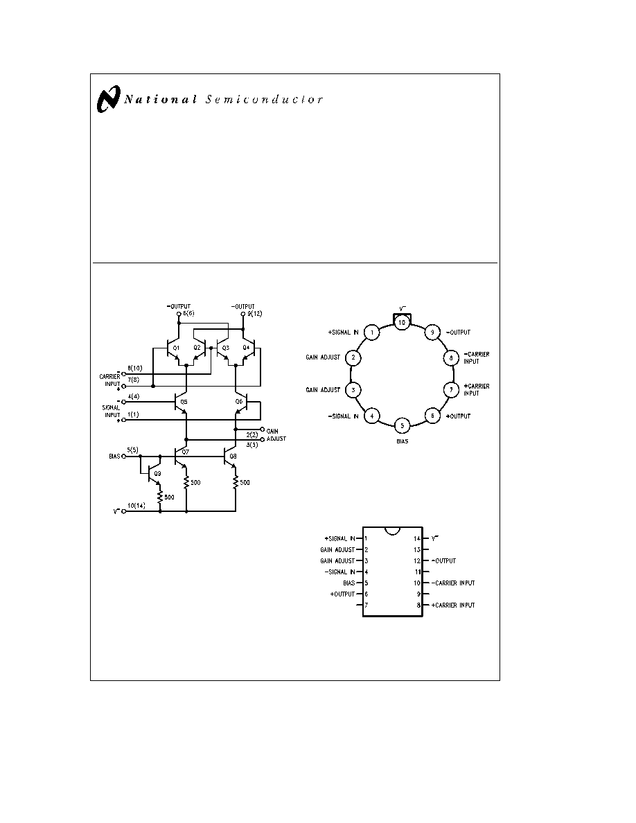
Schematic and Connection Diagrams
TL H 7887 ≠ 1
Numbers in parentheses show DIP connections
Metal Can Package
TL H 7887 ≠ 2
Top View
Note
Pin 10 is connected electrically to the
case through the device substrate
Order Number LM1496H or LM1596H
See NS Package Number H08C
Dual-In-Line and Small Outline Packages
TL H 7887 ≠ 3
Order Number LM1496M or LM1496N
See NS Package Number M14A or N14A
C1995 National Semiconductor Corporation
RRD-B30M115 Printed in U S A
Absolute Maximum Ratings
If Military Aerospace specified devices are required
please contact the National Semiconductor Sales
Office Distributors for availability and specifications
Internal Power Dissipation (Note 1)
500 mW
Applied Voltage (Note 2)
30V
Differential Input Signal (V
7
b
V
8
)
g
5 0V
Differential Input Signal (V
4
b
V
1
)
g
(5
a
I
5
R
0
)V
Input Signal (V
2
b
V
1
V
3
b
V
4
)
5 0V
Bias Current (I
5
)
12 mA
Operating Temperature Range LM1596
b
55 C to
a
125 C
LM1496
0 C to
a
70 C
Storage Temperature Range
b
65 C to
a
150 C
Soldering Information
Dual-In-Line Package
Soldering (10 seconds)
260 C
Small Outline Package
Vapor Phase (60 seconds)
215 C
Infrared (15 seconds)
220 C
See AN-450 ``Surface Mounting Methods and their effects
on Product Reliability'' for other methods of soldering sur-
face mount devices
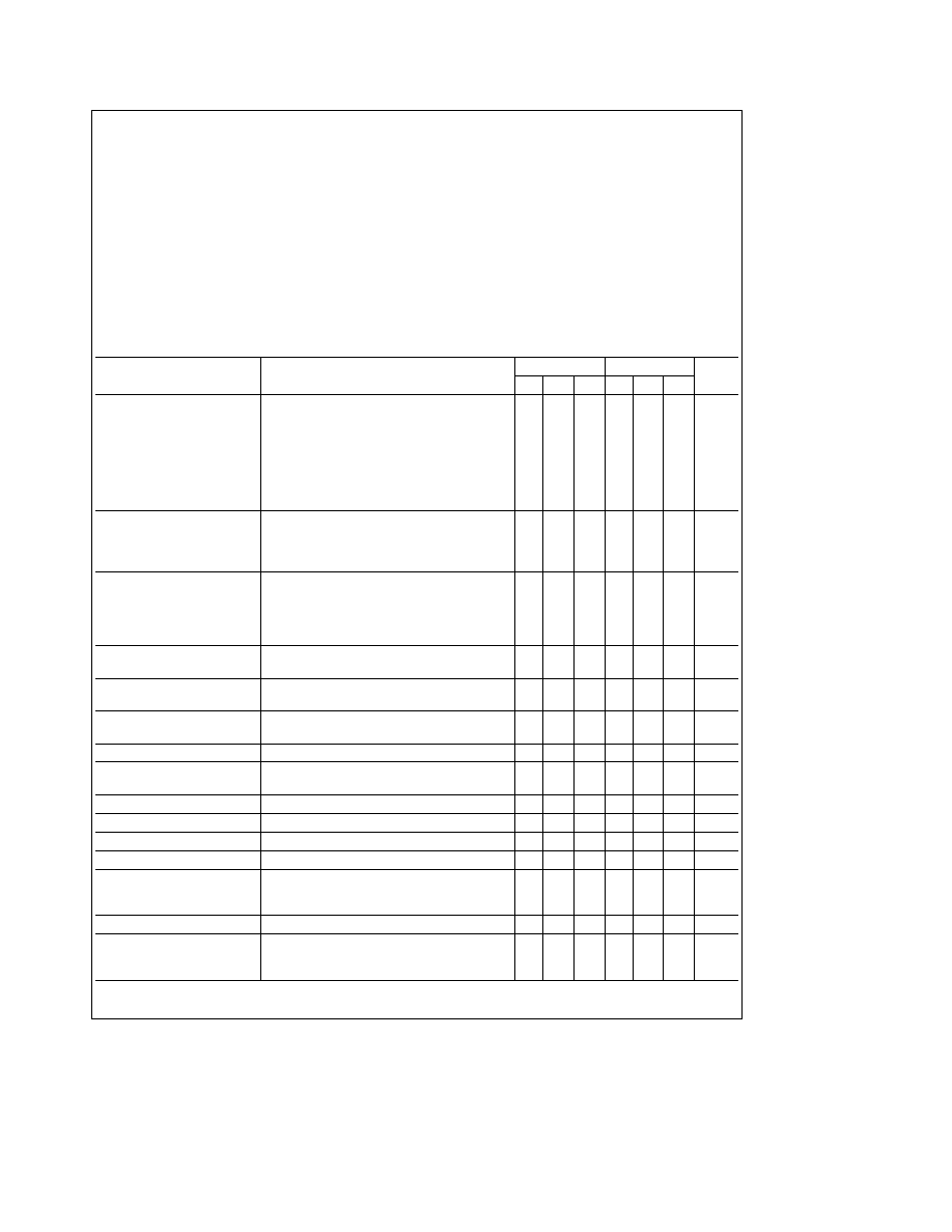
Electrical Characteristics
(T
A
e
25 C unless otherwise specified see test circuit)
Parameter
Conditions
LM1596
LM1496
Units
Min
Typ
Max Min
Typ
Max
Carrier Feedthrough
V
C
e
60 mVrms sine wave
40
40
m
Vrms
f
C
e
1 0 kHz offset adjusted
V
C
e
60 mVrms sine wave
140
140
m
Vrms
f
C
e
10 kHz offset adjusted
V
C
e
300 mV
pp
square wave
0 04
0 2
0 04
0 2
mVrms
f
C
e
1 0 kHz offset adjusted
V
C
e
300 mV
pp
square wave
20
100
20
150
mVrms
f
C
e
1 0 kHz not offset adjusted
Carrier Suppression
f
S
e
10 kHz 300 mVrms
50
65
50
65
dB
f
C
e
500 kHz 60 mVrms sine wave offset adjusted
f
S
e
10 kHz 300 mVrms
50
50
dB
f
C
e
10 MHz 60 mVrms sine wave offset adjusted
Transadmittance Bandwidth
R
L
e
50X
300
300
MHz
Carrier Input Port V
C
e
60 mVrms sine wave
f
S
e
1 0 kHz 300 mVrms sine wave
Signal Input Port V
S
e
300 mVrms sine wave
80
80
MHz
V
7
b
V
8
e
0 5Vdc
Voltage Gain Signal Channel
V
S
e
100 mVrms f
e
1 0 kHz
2 5
3 5
2 5
3 5
V V
V
7
b
V
8
e
0 5 Vdc
Input Resistance Signal Port
f
e
5 0 MHz
200
200
kX
V
7
b
V
8
e
0 5 Vdc
Input Capacitance Signal Port
f
e
5 0 MHz
2 0
2 0
pF
V
7
b
V
8
e
0 5 Vdc
Single Ended Output Resistance f
e
10 MHz
40
40
kX
Single Ended Output
f
e
10 MHz
5 0
5 0
pF
Capacitance
Input Bias Current
(I
1
a
I
4
) 2
12
25
12
30
m
A
Input Bias Current
(I
7
a
I
8
) 2
12
25
12
30
m
A
Input Offset Current
(I
1
b
I
4
)
0 7
5 0
0 7
5 0
m
A
Input Offset Current
(I
7
b
I
8
)
0 7
5 0
5 0
5 0
m
A
Average Temperature
(
b
55 C
k
T
A
k
a
125 C)
2 0
nA C
Coefficient of Input
(0 C
k
T
A
k
a
70 C)
2 0
nA C
Offset Current
Output Offset Current
(I
6
b
I
9
)
14
50
14
60
m
A
Average Temperature
(
b
55 C
k
T
A
k
a
125 C)
90
nA C
Coefficient of Output
(0 C
k
T
A
k
a
70 C)
90
nA C
Offset Current
2
Electrical Characteristics
(T
A
e
25 C unless otherwise specified see test circuit) (Continued)
Parameter
Conditions
LM1596
LM1496
Units
Min
Typ
Max
Min
Typ
Max
Signal Port Common Mode
f
S
e
1 0 kHz
5 0
5 0
V
p-p
Input Voltage Range
Signal Port Common Mode
V
7
b
V
8
e
0 5 Vdc
b
85
b
85
dB
Rejection Ratio
Common Mode Quiescent
8 0
8 0
Vdc
Output Voltage
Differential Output Swing
8 0
8 0
V
p-p
Capability
Positive Supply Current
(I
6
a
I
g
)
2 0
3 0
2 0
3 0
mA
Negative Supply Current
(I
10
)
3 0
4 0
3 0
4 0
mA
Power Dissipation
33
33
mW
Note 1
LM1596 rating applies to case temperatures to
a
125 C derate linearly at 6 5 mW C for ambient temperature above 75 C LM1496 rating applies to case
temperatures to
a
70 C
Note 2
Voltage applied between pins 6-7 8-1 9-7 9-8 7-4 7-1 8-4 6-8 2-5 3-5
Note 3
Refer to rets1596x drawing for specifications of military LM1596H versions
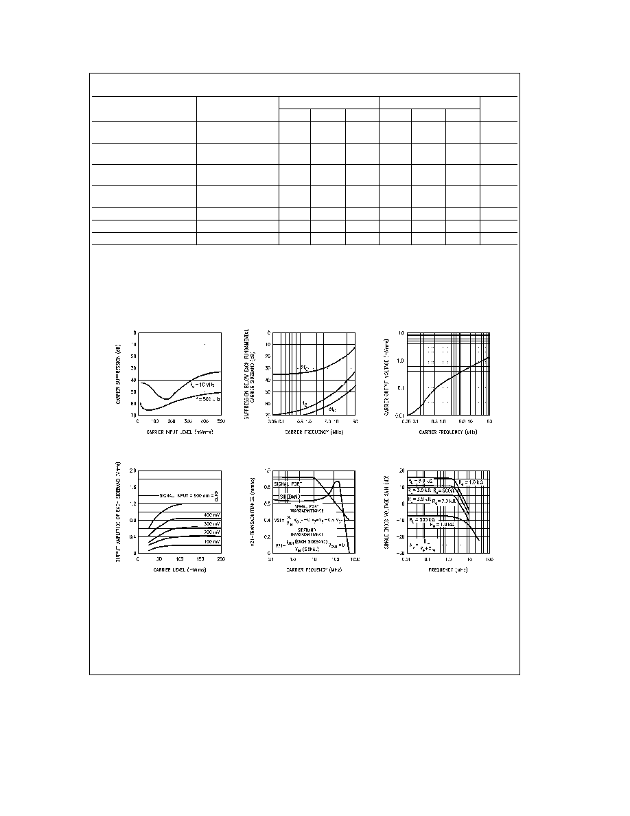
Typical Performance Characteristics
Carrier Input Level
Carrier Suppression vs
Frequency
Carrier Suppression vs
Frequency
Carrier Feedthrough vs
Carrier Levels
Sideband Output vs
Frequency
Transadmittances vs
Sideband and Signal Port
Response
Signal-Port Frequency
TL H 7887 ≠ 5
3

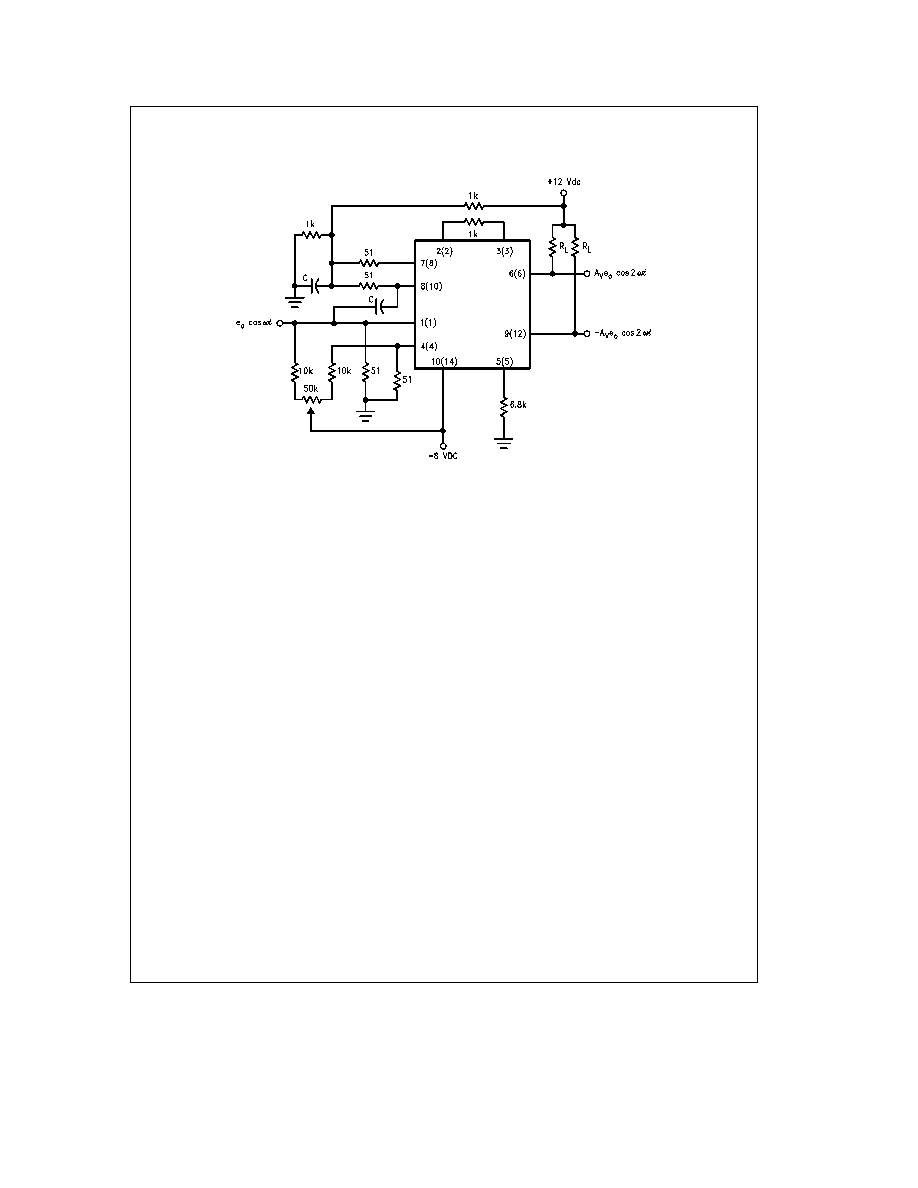
Typical Application and Test Circuit
Suppressed Carrier Modulator
Numbers in parentheses show DIP connections
TL H 7887 ≠ 4
Note
S
1
is closed for ``adjusted'' measurements
SSB Product Detector
Numbers in parentheses show DIP connections
TL H 7887 ≠ 6
This figure shows the LM1596 used as a single sideband (SSB) suppressed carrier demodulator (product detector) The carrier signal is applied to the carrier input
port with sufficient amplitude for switching operation A carrier input level of 300 mVrms is optimum The composite SSB signal is applied to the signal input port
with an amplitude of 5 0 to 500 mVrms All output signal components except the desired demodulated audio are filtered out so that an offset adjustment is not
required This circuit may also be used as an AM detector by applying composite and carrier signals in the same manner as described for product detector
operation
4
Typical Applications
(Continued)
Broadband Frequency Doubler
Numbers in parentheses show DIP connections
TL H 7887 ≠ 7
The frequency doubler circuit shown will double low-level signals with low distortion The value of C should be chosen for low reactance at the operating frequency
Signal level at the carrier input must be less than 25 mV peak to maintain operation in the linear region of the switching differential amplifier Levels to 50 mV peak
may be used with some distortion of the output waveform If a larger input signal is available a resistive divider may be used at the carrier input with full signal
applied to the signal input
5