
TL H 11479
LM747
Dual
Operational
Amplifier
November 1994
LM747
Dual Operational Amplifier
General Description
The LM747 is a general purpose dual operational amplifier
The two amplifiers share a common bias network and power
supply leads Otherwise their operation is completely inde-
pendent
Additional features of the LM747 are no latch-up when in-
put common mode range is exceeded freedom from oscilla-
tions and package flexibility
The LM747C LM747E is identical to the LM747 LM747A
except that the LM747C LM747E has its specifications
guaranteed over the temperature range from 0 C to
a
70 C
instead of
b
55 C to
a
125 C
Features
Y
No frequency compensation required
Y
Short-circuit protection
Y
Wide common-mode and differential voltage ranges
Y
Low power consumption
Y
No latch-up
Y
Balanced offset null
Connection Diagrams
Metal Can Package
TL H 11479 ≠ 4
Order Number LM747H
See NS Package Number H10C
Dual-In-Line Package
TL H 11479 ≠ 5
Order Number LM747CN or LM747EN
See NS Package Number N14A
V
a
A and V
a
B are internally connected
C1995 National Semiconductor Corporation
RRD-B30M115 Printed in U S A

Absolute Maximum Ratings
If Military Aerospace specified devices are required
please contact the National Semiconductor Sales
Office Distributors for availability and specifications
Supply Voltage
LM747 LM747A
g
22V
LM747C LM747E
g
18V
Power Dissipation (Note 1)
800 mW
Differential Input Voltage
g
30V
Input Voltage (Note 2)
g
15V
Output Short-Circuit Duration
Indefinite
Operating Temperature Range
LM747 LM747A
b
55 C to
a
125 C
LM747C LM747E
0 C to
a
70 C
Storage Temperature Range
b
65 C to
a
150 C
Lead Temperature (Soldering 10 sec )
300 C
Electrical Characteristics
(Note 3)
Parameter
Conditions
LM747A LM747E
LM747
LM747C
Units
Min
Typ
Max
Min
Typ
Max
Min
Typ
Max
Input Offset Voltage
T
A
e
25 C
R
S
s
10 kX
1 0
5 0
2 0
6 0
mV
R
S
s
50X
0 8
3 0
R
S
s
50X
4 0
mV
R
S
s
10 kX
6 0
7 5
Average Input Offset
15
m
V C
Voltage Drift
Input Offset Voltage
T
A
e
25 C V
S
e
g
20V
g
10
g
15
g
15
mV
Adjustment Range
Input Offset Current
T
A
e
25 C
3 0
30
20
200
20
200
nA
70
85
500
300
Average Input Offset
0 5
nA C
Current Drift
Input Bias Current
T
A
e
25 C
30
80
80
500
80
500
nA
T
AMIN
s
T
A
s
T
AMAX
0 210
1 5
0 8
m
A
Input Resistance
T
A
e
25 C V
S
e
g
20V
1 0
6 0
0 3
2 0
0 3
2 0
MX
V
S
e
g
20V
0 5
Input Voltage Range
T
A
e
25 C
g
12
g
13
V
g
12
g
13
g
12
g
13
Large Signal
T
A
e
25 C R
L
t
2 kX
Voltage Gain
V
S
e
g
20V V
O
e
g
15V
50
V mV
V
S
e
g
15V V
O
e
g
10V
50
200
20
200
V mV
R
L
t
2 kX
V
S
e
g
20V V
O
e
g
15V
32
V mV
V
S
e
g
15V V
O
e
g
10V
25
15
V mV
V
S
e
g
5V V
O
e
g
2V
10
V mV
Output Voltage Swing
V
S
e
g
20V
R
L
t
10 kX
g
16
V
R
L
t
2 kX
g
15
V
S
e
g
15V
R
L
t
10 kX
g
12
g
14
g
12
g
14
V
R
L
t
2 kX
g
10
g
13
g
10
g
13
Output Short
T
A
e
25 C
10
25
35
25
25
mA
Circuit Current
10
40
Common-Mode
R
S
s
10 kX V
CM
e
g
12V
70
90
70
90
dB
Rejection Ratio
R
S
s
50 kX V
CM
e
g
12V
80
95
2
Electrical Characteristics
(Note 3) (Continued)
Parameter
Conditions
LM747A LM747E
LM747
LM747C
Units
Min
Typ
Max
Min
Typ
Max
Min
Typ
Max
Supply Voltage
V
S
e g
20V to V
S
e g
5V
Rejection Ratio
R
S
s
50X
86
96
dB
R
S
s
10 kX
77
96
77
96
Transient Response
T
A
e
25 C Unity Gain
Rise Time
0 25
0 8
0 3
0 3
m
s
Overshoot
6 0
20
5
5
%
Bandwidth (Note 4)
T
A
e
25 C
0 437
1 5
MHz
Slew Rate
T
A
e
25 C Unity Gain
0 3
0 7
0 5
0 5
V ms
Supply Current Amp
T
A
e
25 C
2 5
1 7
2 8
1 7
2 8
mA
Power Consumption Amp
T
A
e
25 C
V
S
e g
20V
80
150
mW
V
S
e g
15V
50
85
50
85
LM747A
V
S
e g
20V
T
A
e
T
AMIN
165
mW
T
A
e
T
AMAX
135
LM747E
V
S
e g
20V
150
T
A
e
T
AMIN
150
mW
T
A
e
T
AMAX
150
LM747
V
S
e g
15V
T
A
e
T
AMIN
60
100
mW
T
A
e
T
AMAX
45
75
Note 1
The maximum junction temperature of the LM747C LM747E is 100 C For operating at elevated temperatures devies in the TO-5 package must be
derated based on a thermal resistance of 150 C W junction to ambient or 45 C W junction to case The thermal resistance of the dual-in-line package is 100 C
W junction to ambient
Note 2
For supply voltages less than
g
15V the absolute maximum input voltage is equal to the supply voltage
Note 3
These specifications apply for
g
5V
s
V
S
s g
20V and
b
55 C
s
T
A
s
125 C for the LM747A and 0 C
s
T
A
s
70 C for the LM747E unless otherwise
specified The LM747 and LM747C are specified for V
S
e g
15V and
b
55 C
s
T
A
s
125 C and 0 C
s
T
A
s
70 C respectively unless otherwise specified
Note 4
Calculated value from 0 35 Rise Time (ms)
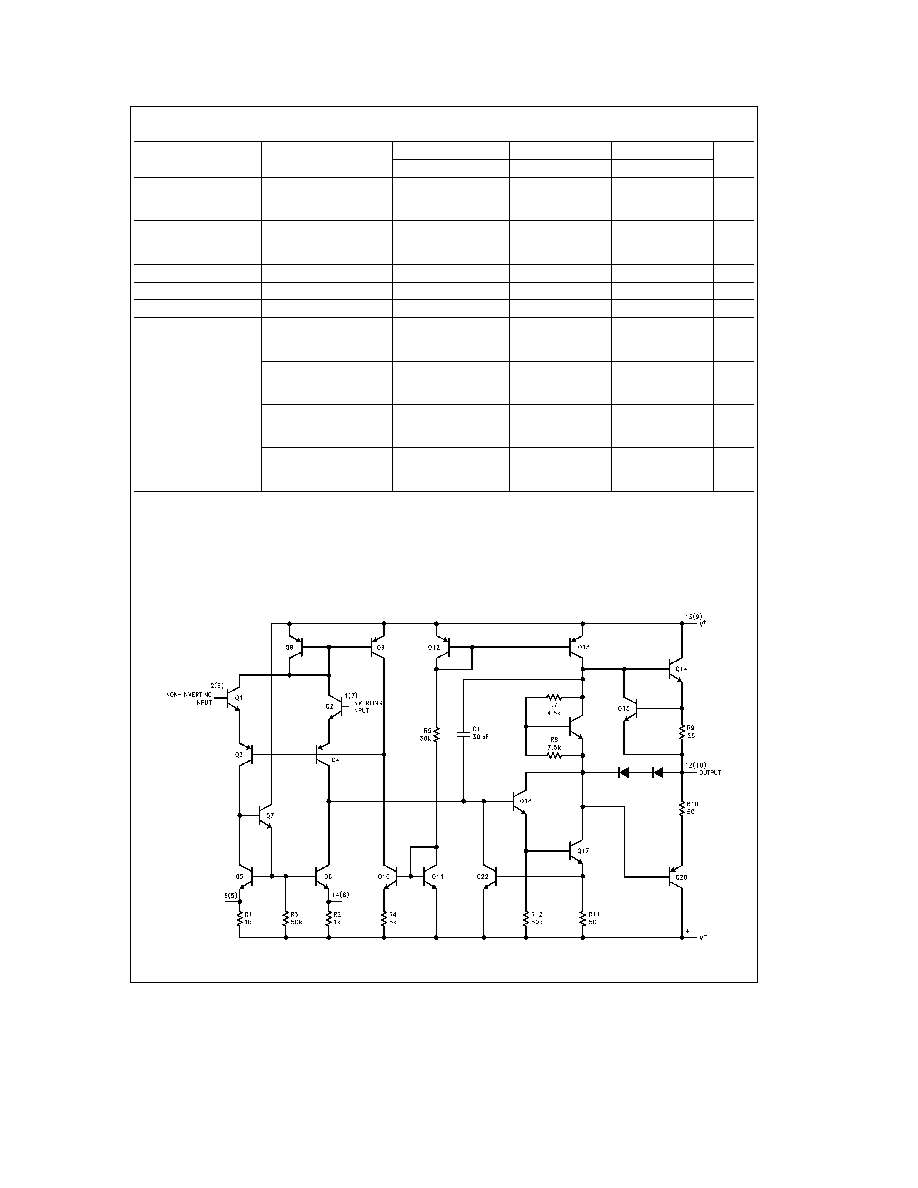
Schematic Diagram
(Each Amplifier)
TL H 11479 ≠ 1
Note
Numbers in parentheses are pin numbers for amplifier B DIP only
3
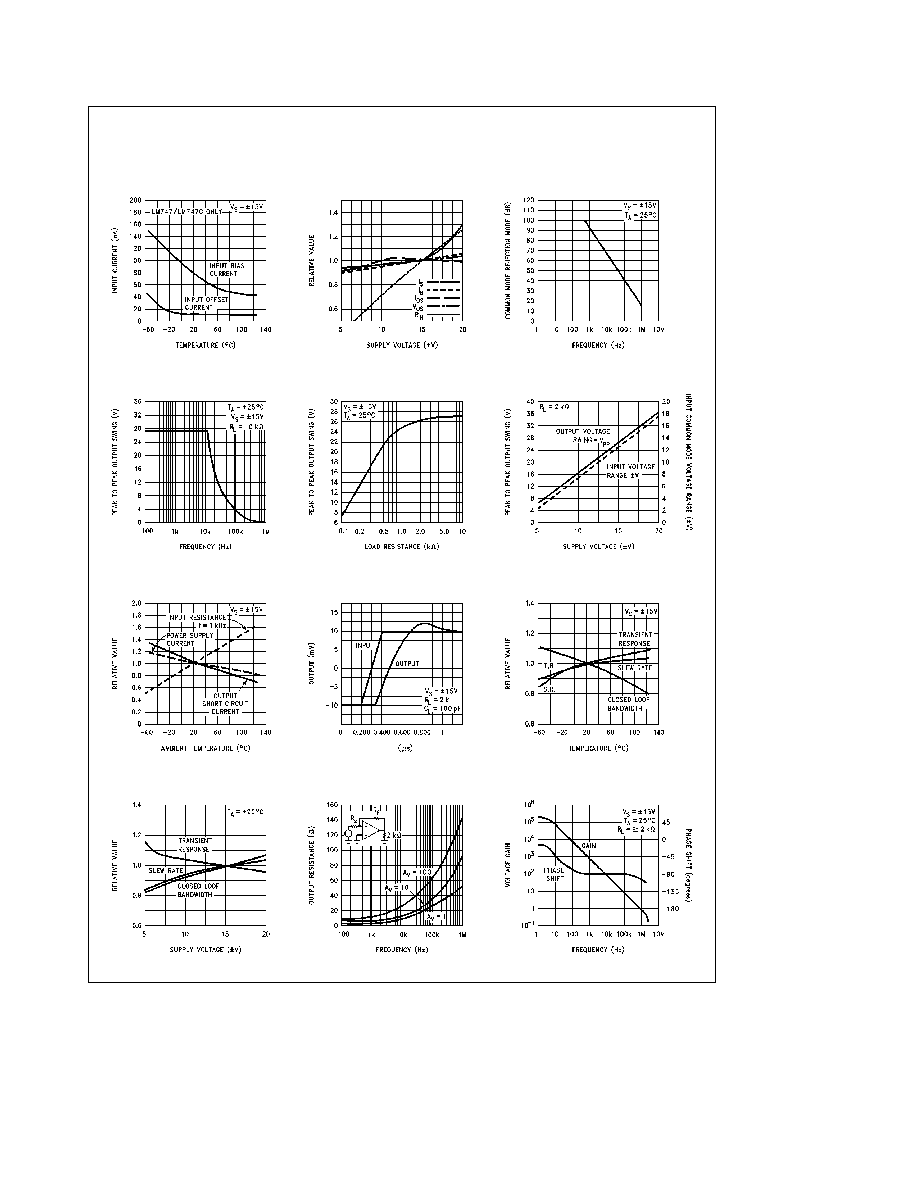
Typical Performance Characteristics
Temperature
Currents vs Ambient
Input Bias and Offset
vs Supply Voltage
DC Parameters
Ratio vs Frequency
Common Mode Rejection
vs Frequency
Output Voltage Swing
vs Load Resistance
Output Voltage Swing
Supply Voltage
Input Range vs
Output Swing and
vs Ambient Temperature
Normalized DC Parameters
Transient Response
vs Ambient Temperature
Frequency Characteristics
vs Supply Voltage
Frequency Characteristics
vs Frequency
Output Resistance
Characteristics vs Frequency
Open Loop Transfer
TL H 11479 ≠ 2
4
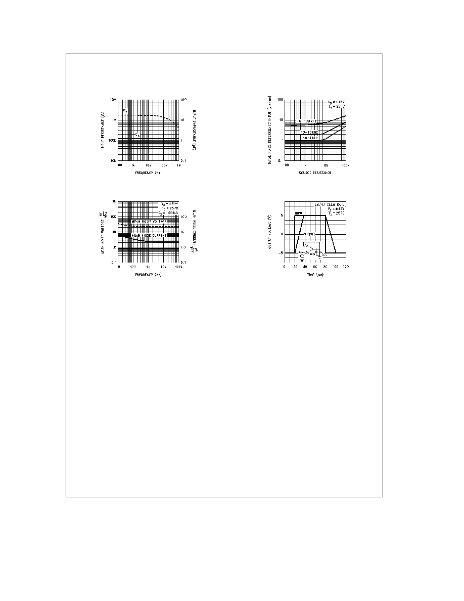
Typical Performance Characteristics
(Continued)
vs Frequency
Input Capacitance
Input Resistance and
Various Bandwidths
Broadband Noise for
vs Frequency
and Current
Input Noise Voltage
Signal Pulse Response
Voltage Follower Large
TL H 11479 ≠ 3
5