 | ÐлекÑÑоннÑй компоненÑ: LM169 | СкаÑаÑÑ:  PDF PDF  ZIP ZIP |
Äîêóìåíòàöèÿ è îïèñàíèÿ www.docs.chipfind.ru
TL H 9110
LM169LM369
Precision
Voltage
Reference
December 1994
LM169 LM369 Precision Voltage Reference
General Description
The LM169 LM369 are precision monolithic temperature-
compensated voltage references They are based on a bur-
ied zener reference as pioneered in the LM199 references
but do not require any heater as they rely on special tem-
perature-compensation techniques (Patent Pending) The
LM169 makes use of thin-film technology enhanced by the
discrete laser trimming of resistors to achieve excellent
Temperature coefficient (Tempco) of V
out
(as low as 1
ppm C) along with tight initial tolerances (as low as 0 05%
max) The trim scheme is such that individual resistors are
cut open rather than being trimmed (partially cut) to avoid
resistor drift caused by electromigration in the trimmed area
The LM169 also provides excellent stability vs changes in
input voltage and output current (both sourcing and sinking)
The devices have a 10 000V output and will operate in ei-
ther series or shunt mode the output is short-circuit-proof to
ground A trim pin is available which permits fine-trimming of
V
out
and also permits filtering to greatly decrease the out-
put noise by adding a small capacitor (0 05 to 0 5 mF)
Features
Y
Low Tempco
3 ppm C (max)
Y
Excellent initial accuracy
g
5 mV (max)
Y
Excellent line regulation
4 ppm V (max)
Y
Excellent output impedance
g
0 8X (max)
Y
Excellent thermal regulation
g
20 ppm 100 mW (max)
Y
Low noise
Y
Easy to filter output noise
Y
Operates in series or shunt mode
Applications
Y
High-Resolution Data Acquisition Systems
Y
Digital volt meters
Y
Weighing systems
Y
Precision current sources
Y
Test Equipment
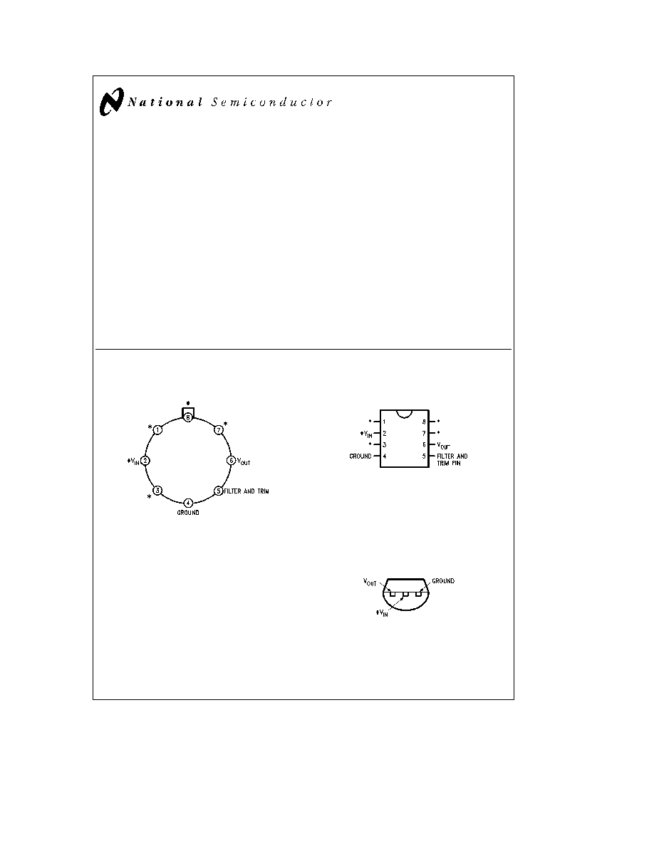
Connection Diagrams
Metal Can Package (H)
TL H 9110 1
Top View
(Case is connected to ground )
Do not connect internal connection for factory trims
Order Number LM169H LM169BH
LM169H 883 LM369H or LM369BH
See NS Package Number H08C
Dual-In-Line Package (N)
or S O Package (M)
TL H 9110 5
Top View
Order Number LM369DM LM369DMX
LM369N
LM369BN LM369CN or LM369DN
See NS Package Number M08A or N08E
X denotes 2500 units on Tape and Reel and is not included in the device
part number marking
TO-226 Plastic Package (RC)
TL H 9110 28
Bottom View
Order Number LM369DRC
See NS Package Number RC03A
Teflon
and Mylar
are registered trademarks of E I DuPont Corp
C1995 National Semiconductor Corporation
RRD-B30M115 Printed in U S A
Absolute Maximum Ratings
(Note 8)
If Military Aerospace specified devices are required
please contact the National Semiconductor Sales
Office Distributors for availability and specifications
Input Voltage (Series Mode)
35V
Reverse Current (Shunt Mode)
50 mA
Power Dissipation (Note 7)
600 mW
Storage Temperature Range
b
60 C to
a
150 C
Operating Temperature Range
(T
j
min to T
j
max)
LM169H LM169H 883
b
55 C to
a
125 C
LM369
0 C to
a
70 C
Soldering Information
DIP (N) or Plastic (RC) Package 10 sec
a
260 C
H08 (H) Package 10 sec
a
300 C
SO (M) Package Vapor Phase (60 sec )
a
215 C
Infrared (15 sec )
a
220 C
See AN-450 ``Surface Mounting Methods and Their Effect
on Product Reliability'' (Appendix D) for other methods of
soldering surface mount devices
ESD Tolerance
C
zap
e
100 pF R
zap
e
1 5k
800V
Electrical Characteristics LM169 LM369
(Note 1)
Tested
Design
Units
Parameter
Conditions
Typical
Limits
Limit
(Max
(Notes 2 13)
(Note 3)
Unless
Noted)
V
out
Nominal
a
10 000
V
V
out
Error
(Note 11)
50
g
500
ppm
0 50
g
5
mV
V
out
Tempco
LM169B LM369B
T
min
k
T
j
k
T
max
1 0
3 0
ppm C
LM169 LM369
T
min
k
T
j
k
T
max
2 7
5 0
ppm C
LM369C
T
min
k
T
j
k
T
max
6
10
ppm C
(Note 6) (Note 11)
Line Regulation
13V
s
V
IN
s
30V
2 0
4 0
8 0
ppm V
Load Regulation
Sourcing
0 to 10 mA
a
3
g
8 0
20 0
ppm mA
Sinking (Note 12)
0 to
b
10 mA
a
80
a
150
ppm mA
(Note 4 Note 9)
Thermal Regulation
(t
e
10 msec
Sourcing
After Load
3 0
g
20
ppm 100 mW
Sinking (Note 12)
is Applied)
3 0
ppm 100 mW
(Note 5)
Supply Current
1 4
1 8
2 0
mA
D
Supply Current
13V
s
V
IN
s
30V
0 06
0 12
0 2
mA
Short Circuit
27
15
11
mA min
Current
50
65
mA max
Noise Voltage
10 Hz to 1 kHz
10
30
m
V rms
0 1 Hz to 10 Hz
4
m
V p-p
(10 Hz to 10 kHz
4
m
V rms
C
filter
e
0 1 mF)
Long-term
1000 hours
6
ppm
Stability
T
j
k
T
max
(Non-Cumulative)
(Measured at
(Note 10)
a
25 C)
Temperature
D
T
e
25 C
3
ppm
Hysteresis of V
out
Output Shift
1500
2600
ppm
per 1 mA at Pin 5
2
Electrical Characteristics LM369D
(Note 1)
Tested
Design
Units
Parameter
Conditions
Typical
Limits
Limit
(Max
(Notes 2 13)
(Note 3)
Unless
Noted)
V
out
Nominal
a
10 000
V
V
out
Error
70
g
1000
ppm
LM369D
0 7
g
10 0
mV
V
out
Tempco
T
min
s
T
j
s
T
max
5
30
ppm C
(Note 6)
Line Regulation
13V
s
V
IN
s
30V
2 4
g
6 0
12
ppm V
Load Regulation
Sourcing
0 to 10 mA
a
3
g
12
g
25
ppm mA
Sinking (Note 12)
0 to
b
10 mA
a
80
a
160
ppm mA
(Note 4 Note 9)
Thermal Regulation
(t
e
10 msec
Sourcing
After Load
4 0
g
25
ppm 100 mW
Sinking (Note 12)
is Applied)
4 0
ppm 100 mW
(Note 5)
Supply Current
1 5
2 0
2 4
mA
D
Supply Current
13V
s
V
IN
s
30V
0 06
0 16
0 3
mA
Short Circuit
27
14
10
mA min
Current
50
65
mA max
Noise Voltage
10 Hz to 1 kHz
10
30
m
V rms
0 1 Hz to 10 Hz
4
m
V p-p
(10 Hz to 10 kHz
4
m
V rms
C
filter
e
0 1 mF)
Long-Term
1000 Hours
8
ppm
Stability
T
j
k
T
max
(Non-Cumulative)
(Measured at
a
25 C)
Temperature
D
T
e
25 C
5
ppm
Hysteresis of V
out
Output Shift
1500
2800
ppm
Per 1 mA at Pin 5
Note 1
Unless otherwise noted these conditions apply T
j
e a
25 C 13V
s
V
in
s
17V 0
s
I
load
s
1 0 mA C
L
e s
200 pF Specifications in BOLDFACED
TYPE apply over the rated operating temperature range
Note 2
Tested limits are guaranteed and 100% tested in production
Note 3
Design Limits are guaranteed (but not 100% production tested) over the indicated temperature and supply voltage ranges These limits are not to be used
to calculate outgoing quality levels
Note 4
The LM169 has a Class B output and will exhibit transients at the crossover point This point occurs when the device is required to sink approximately 1 0
mA In some applications it may be advantageous to pre-load the output to either V
in
or to ground to avoid this crossover point
Note 5
Thermal regulation is defined as the change in the output voltage at a time T after a step change of power dissipation of 100 mW
Note 6
Temperature Coefficient of V
OUT
is defined as the worst-case DV
out
measured at Specified Temperatures divided by the total span of the Specified
Temperature Range (see graphs) There is no guarantee that the Specified Temperatures are exactly at the minimum or maximum deviation
Note 7
In metal can (H) i
J-C
is 75 C W and i
J-A
is 150 C W In plastic DIP i
J-A
is 160 C W In S0-8 i
J-A
is 180 C W in TO-226 i
J-A
is 160 C W
Note 8
Absolute Maximum Ratings indicate limits beyond which damage to the device may occur DC and AC electrical specifications are not guaranteed beyond
the Rated Operating Conditions
Note 9
Regulation is measured at constant temperature using pulse testing with a low duty cycle Changes in output voltage due to heating effects are covered
under the specifications for Thermal Regulation and Tempco Load Regulation is measured at a point on the output pin 1 8
below the bottom of the package
Note 10
Consult factory for availability of devices with Guaranteed Long-term Stability
Note 11
Consult factory for availability of devices with tighter Accuracy and Tempco Specifications
Note 12
In Sinking mode connect 0 1 mF tantalum capacitor from output to ground
Note 13
A military RETS electrical test specification is available on request
3
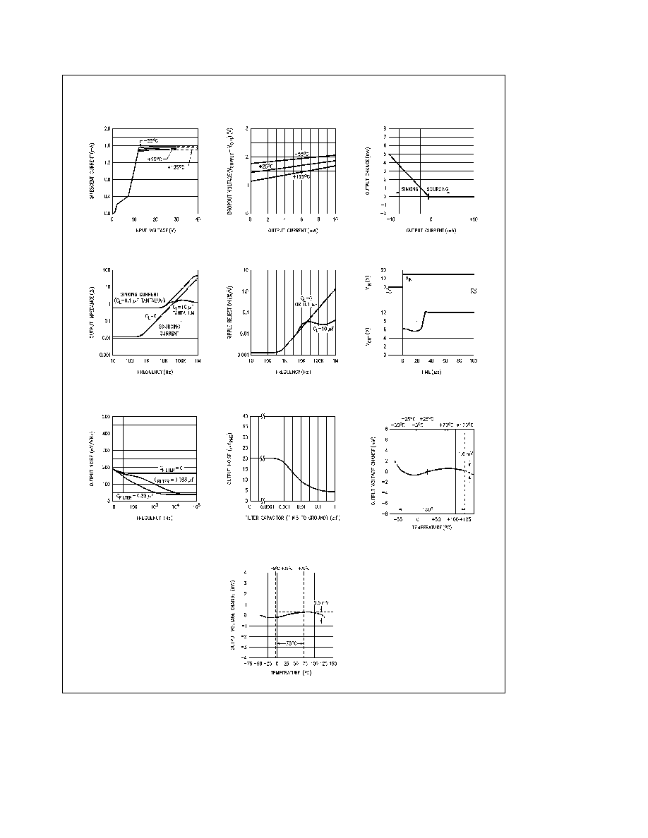
Typical Performance Characteristics
(Note 1)
Voltage and Temperature
Quiescent Current vs Input
Mode Sourcing Current)
Output Current (Series
Dropout Voltage vs
Output Current
Output Change vs
vs Frequency
Output Impedance
vs Frequency
Ripple Rejection
Start-up Response
TL H 9110 6
Output Noise vs Frequency
TL H 9110 24
Output Noise vs Filter
Capacitor
TL H 9110 25
Coefficient Specified
LM169 Temperature
Temperatures (see Note 6)
TL H 9110 26
Coefficient Specified
LM369 Temperature
Temperatures (see Note 6)
TL H 9110 27
Typical Temperature Coefficient Calculations
LM169 (see curve above)
T C
e
1 6 mV (180
c
10V)
e
8 9
c
10
b
7 e
0 89 ppm C
LM369 (see curve at left)
T C
e
0 5 mV (75
c
10V)
e
6 7
c
10
b
7 e
0 67 ppm C
4

Application Hints
The LM169 LM369 can be applied in the same way as any
other voltage reference The adjacent Typical Applications
Circuits suggest various uses for the LM169 LM369 The
LM169 is recommended for applications where the highest
stability and lowest noise is required over the full military
temperature range The LM369 is suitable for limited-tem-
perature operation The curves showing the Noise vs Ca-
pacitance in the Typical Performance Characteristics sec-
tion show graphically that a modest capacitance of 0 1 to
0 3 microfarads can cut the broadband noise down to a lev-
el of only a few microvolts less than 1 ppm of the output
voltage The capacitor used should be a low-leakage type
For the temperature range 0 to 50 C polyester or Mylar
will be suitable but at higher temperatures a premium film
capacitor such as polypropylene is recommended For oper-
ation at
a
125 C a Teflon
capacitor would be required to
ensure sufficiently low leakage Ceramic capacitors may
seem to do the job but are not recommended for produc-
tion use as the high-K ceramics cannot be guaranteed for
low leakage and may exhibit piezo-electric effects convert-
ing vibration or mechanical stress into excessive electrical
noise
Additionally the inherent superiority of the LM169 369's
buried Zener diode provides freedom from low-frequency
noise wobble and jitter in the frequency range 0 01 to 10
Hertz where capacitive filtering is not feasible
Pins 1 3 7 and 8 of the LM169 369 are connected to
internal trim circuits which are used to trim the device's out-
put voltage and Tempco during final testing at the factory
Do not connect anything to these pins or improper opera-
tion may result These pins would not be damaged by a
short to ground or by Electrostatic Discharges however
keep them away from large transients or AC signals as
stray capacitance could couple noises into the output
These pins may be cut off if desired Alternatively a shield
foil can be laid out on the printed circuit board surrounding
these pins and pin 5 and this guard foil can be connected to
ground or to V
out
effectively acting as a guard against AC
coupling and DC leakages
The trim pin (pin 5) should also be guarded away from noise
signals and leakages as it has a sensitivity of 15 millivolts of
D
V
out
per microampere The trim pin can also be used in
the circuits shown to provide an output trim range of
g
10
millivolts Trimming to a wider range is possible but is not
recommended as it may degrade the Tempco and the
Tempco linearity at temperature extremes For example if
the output were trimmed up to 10 240V the Tempco would
be degraded by 8 ppm C As a general rule Tempco will
be degraded by 1 ppm C per 30 mV of output adjustment
The output can sink current as well as source it but the
output impedance is much better for sourcing current Also
the LM169 369 requires a 0 1 mF tantalum capacitor (or
0 1 mF in series with 10X) bypass from the output to ground
for stable operation in shunt mode (output sinking current)
The output has a class-B stage so if the load current chang-
es from sourcing to sinking an output transient will occur
To avoid this transient it may be advisable to preload the
output with a few milliamperes of load to ground The
LM169 369 does have an excellent tolerance of load ca-
pacitance and in cases of load transients electrolytic or
tantalum capacitors in the range 1 to 500 microfarads have
been shown to improve the output impedance without de-
grading the dynamic stability of the device The LM169 369
are rated to drive an output of
g
10 mA but for best accura-
cy any load current larger than 1 mA can cause thermal
errors (such as 1 mA
c
5V
c
4 ppm 100 mW
e
0 2 ppm
or 2 microvolts) and degrade the ultimate precision of the
output voltage
The output is short-circuit-proof to ground However avoid
overloads at high ambient temperatures as a prolonged
short-circuit may cause the junction temperature to exceed
the Absolute Maximum Temperature The device does not
include a thermal shut-down circuit If the output is pulled to
a positive voltage such as
a
15 or
a
20V the output current
will be limited but overheating may occur Avoid such over-
loads for voltages higher than
a
20 V for more than 5 sec-
onds or at high ambient temperatures
The LM169 369 has an excellent long-term stability and is
suitable for use in high-resolution Digital Voltmeters or Data
Acquisition systems Its long-term stability is typically 3 to 10
ppm per 1000 hours when held near T
max
and slightly bet-
ter when operated at room temperature Contact the factory
for availability of devices with proven long-term stability
Typical Applications
Series Reference
TL H 9110 2
Shunt Reference with Optional Trim
TL H 9110 3
Series Reference with
Optional Filter
for Reduced Noise
TL H 9110 4
NOTE
Pin numbers for H M or N packages
5