LM1851 Ground Fault Interrupter
TL H 5177
LM1851
Ground
Fault
Interrupter
June 1992
LM1851 Ground Fault Interrupter
General Description
The LM1851 is designed to provide ground fault protection
for AC power outlets in consumer and industrial environ-
ments Ground fault currents greater than a presettable
threshold value will trigger an external SCR-driven circuit
breaker to interrupt the AC line and remove the fault condi-
tion In addition to detection of conventional hot wire to
ground faults the neutral fault condition is also detected
Full advantage of the U S UL943 timing specification is tak-
en to insure maximum immunity to false triggering due to
line noise Special features include circuitry that rapidly re-
sets the timing capacitor in the event that noise pulses intro-
duce unwanted charging currents and a memory circuit that
allows firing of even a sluggish breaker on either half-cycle
of the line voltage when external full-wave rectification is
used
Features
Y
Internal power supply shunt regulator
Y
Externally programmable fault current threshold
Y
Externally programmable fault current integration time
Y
Direct interface to SCR
Y
Operates under line reversal both load vs line and hot
vs neutral
Y
Detects neutral line faults
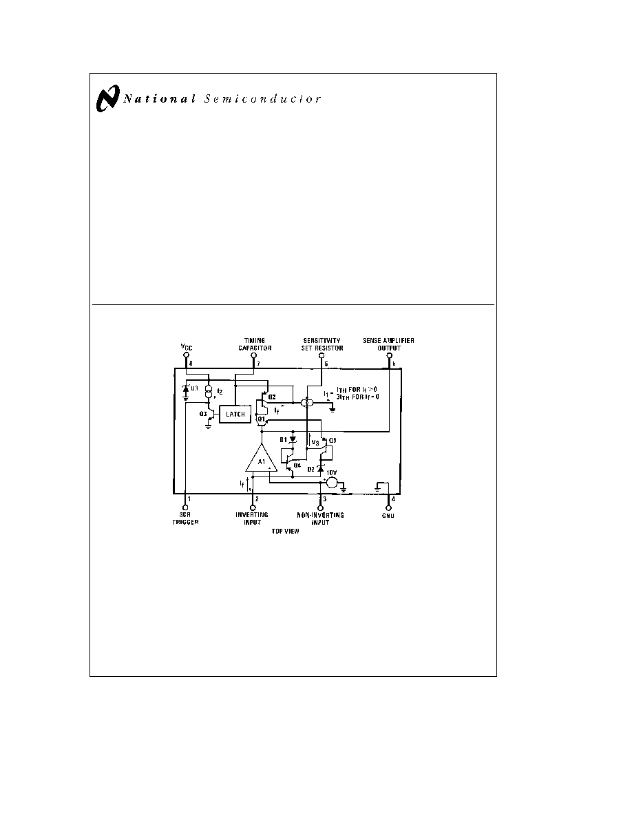
Block and Connection Diagram
TL H 5177 � 1
Order Number LM1851M or LM1851N
See NS Package Number M08A or N08E
C1995 National Semiconductor Corporation
RRD-B30M115 Printed in U S A
Absolute Maximum Ratings
If Military Aerospace specified devices are required
please contact the National Semiconductor Sales
Office Distributors for availability and specifications
Supply Current
19 mA
Power Dissipation (Note 1)
1250 mW
Operating Temperature Range
b
40 C to
a
70 C
Storage Temperature Range
b
55 C to
a
150 C
Soldering Information
Dual-In-Line Package (10 sec )
260 C
Small Outline Package
Vapor Phase (60 sec )
215 C
Infrared (15 sec )
220 C
See AN-450 ``Surface Mounting and Their Effects on Prod-
uct Reliability'' for other methods of soldering surface
mount devices
DC Electrical Characteristics
T
A
e
25 C I
SS
e
5 mA
Parameter
Conditions
Min
Typ
Max
Units
Power Supply Shunt
Pin 8 Average Value
22
26
30
V
Regulator Voltage
Latch Trigger Voltage
Pin 7
15
17 5
20
V
Sensitivity Set Voltage
Pin 8 to Pin 6
6
7
8 2
V
Output Drive Current
Pin 1 With Fault
0 5
1
2 4
mA
Output Saturation Voltage
Pin 1 Without Fault
100
240
mV
Output Saturation Resistance
Pin 1 Without Fault
100
X
Output External Current
Pin 1 Without Fault
2 0
5
mA
Sinking Capability
V
pin 1
Held to 0 3V (Note 4)
Noise Integration
Pin 7 Ratio of Discharge
Sink Current Ratio
Currents Between No Fault
2 0
2 8
3 6
m
A mA
and Fault Conditions
AC Electrical Characteristics
T
A
e
25 C I
SS
e
5 mA
Parameter
Conditions
Min
Typ
Max
Units
Normal Fault Current
Figure 1 (Note 3)
3
5
7
mA
Sensitivity
Normal Fault Trip Time
500X Fault
Figure 2 (Note 2)
18
ms
Normal Fault with
500X Normal Fault
18
ms
Grounded Neutral Fault
2X Neutral
Figure 2 (Note 2)
Trip Time
Note 1
For operation in ambient temperatures above 25 C the device must be derated based on a 125 C maximum junction temperature and a thermal resistance
of 80 C W junction to ambient for the DIP and 162 C W for the SO Package
Note 2
Average of 10 trials
Note 3
Required UL sensitivity tolerance is such that external trimming of LM1851 sensitivity will be necessary
Note 4
This externally applied current is in addition to the internal ``output drive current'' source
TL H 5177 � 2
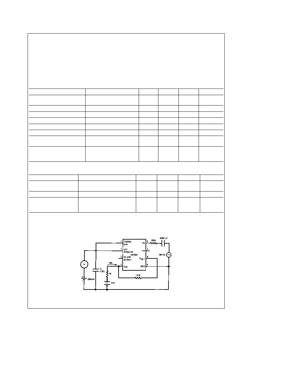
FIGURE 1 Normal Fault Sensitivity Test Circuit
2
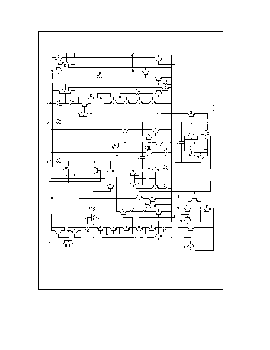
Internal Schematic Diagram
TL H 5177 � 3
3
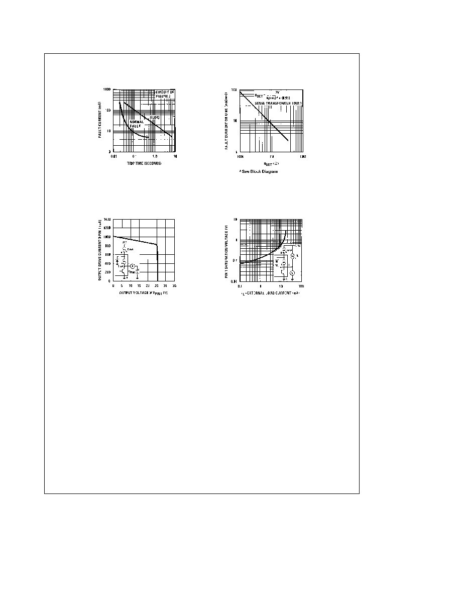
Typical Performance Characteristics
Average Trip Time vs
Normal Fault Current
Threshold vs R
SET
Fault Current
Output Drive Current vs
Pin 1 Saturation Voltage vs
External Load Current I
L
Output Voltage
TL H 5177 � 4
Circuit Description
(Refer to Block and Connection Diagram)
The LM1851 operates from 26V as set by an internal shunt
regulator D3 In the absence of a fault (I
f
e
0) the feedback
path status signal (V
S
) is correspondingly zero Under these
conditions the capacitor discharge current I
1
sits quies-
cently at three times its threshold value I
TH
so that noise
induced charge on the timing capacitor will be rapidly re-
moved When a fault current I
f
is induced in the secondary
of the external sense transformer the operational amplifier
A1 uses feedback to force a virtual ground at the input as it
extracts I
f
The presence of I
f
during either half-cycle will
cause V
S
to go high which in turn changes I
1
from 3I
TH
to
I
TH
Although I
TH
discharges the timing capacitor during
both half-cycles of the line I
f
only charges the capacitor
during the half-cycle in which I
f
exits pin 2 Thus during one
half-cycle I
f
� I
TH
charges the timing capacitor while during
the other half-cycle I
TH
discharges it When the capacitor
voltage reaches 17 5V the latch engages and turns off Q3
permitting I
2
to drive the gate of an SCR
4
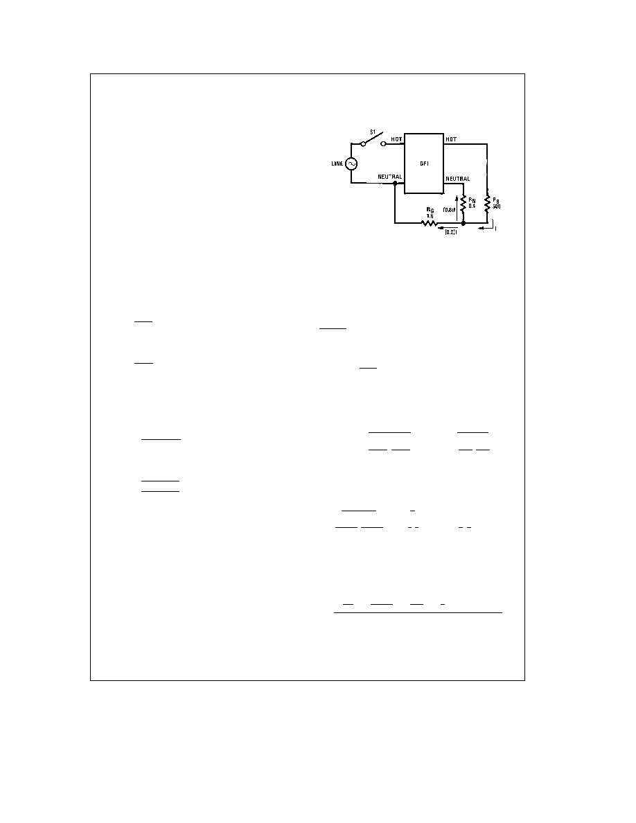
Application Circuits
A typical ground fault interrupter circuit is shown in
Figure 2
It is designed to operate on 120 V
AC
line voltage with 5 mA
normal fault sensitivity
A full-wave rectifier bridge and a 15k 2W resistor are used
to supply the DC power required by the IC A 1 mF capacitor
at pin 8 used to filter the ripple of the supply voltage and is
also connected across the SCR to allow firing of the SCR on
either half-cycle When a fault causes the SCR to trigger
the circuit breaker is energized and line voltage is removed
from the load At this time no fault current flows and the IC
discharge current increases from I
TH
to 3I
TH
(see Circuit
Description and Block Diagram) This quickly resets both
the timing capacitor and the output latch At this time the
circuit breaker can be reset and the line voltage again sup-
plied to the load assuming the fault has been removed A
1000 1 sense transformer is used to detect the normal fault
The fault current which is basically the difference current
between the hot and neutral lines is stepped down by 1000
and fed into the input pins of the operational amplifier
through a 10 mF capacitor The 0 0033 mF capacitor be-
tween pin 2 and pin 3 and the 200 pF between pins 3 and 4
are added to obtain better noise immunity The normal fault
sensitivity is determined by the timing capacitor discharging
current I
TH
I
TH
can be calculated by
I
TH
e
7V
R
SET
d
2
(1)
At the decision point the average fault current just equals
the threshold current I
TH
I
TH
e
I
f(rms)
2
c
0 91
(2)
where I
f(rms)
is the rms input fault current to the operational
amp and the factor of 2 is due to the fact that I
f
charges the
timing capacitor only during one half-cycle while I
TH
dis-
charges the capacitor continuously The factor 0 91 con-
verts the rms value to an average value Combining equa-
tions (1) and (2) we have
R
SET
e
7V
I
f(rms)
c
0 91
(3)
For example to obtain 5 mA(rms) sensitivity for the circuit in
Figure 2 we have
R
SET
e
7V
5 mA
c
0 91
1000
e
1 5M X
(4)
The correct value for R
SET
can also be determined from the
characteristic curve that plots equation (3) Note that this is
an approximate calculation the exact value of R
SET
de-
pends on the specific sense transformer used and LM1851
tolerances Inasmuch as UL943 specifies a sensitivity ``win-
dow'' of 4 mA � 6 mA provision should be made to adjust
R
SET
on a per-product basis
Independent of setting sensitivity the desired integration
time can be obtained through proper selection of the timing
capacitor C
t
Due to the large number of variables involved
proper selection of C
t
is best done empirically The following
design example then should only be used as a guideline
Assume the goal is to meet UL943 timing requirements
Also assume that worst case timing occurs during GF1
start-up (S1 closure) with both a heavy normal fault and a
2X grounded neutral fault present This situation is shown dia-
gramatically below
TL H 5177 � 5
UL943 specifies
s
25 ms average trip time under these con-
ditions Calculation of C
t
based upon charging currents due
to normal fault only is as follows
s
25 ms Specification
b
3 ms GFI turn-on time (15k and 1 mF)
b
8 ms Potential loss of one half-cycle due to fault current
sense of half-cycles only
b
4 ms Time required to open a sluggish circuit breaker
s
10 ms Maximum integration time that could be allowed
8 ms Value of integration time that accommodates com-
ponent tolerances and other variables
C
t
e
I
c
T
V
(5)
where T
e
integration time
V
e
threshold voltage
I
e
average fault current into C
t
I
e
120 V
AC(rms)
R
B
J
c
R
N
R
G
a
R
N
J
X
Y
X
Y
heavy fault
portion of
current generated
fault current
(swamps I
TH
)
shunted
around GFI
c
1 turn
1000 turns
J
c
1
2
J
c
(0 91)
(6)
X
Y X Y
X Y
current
C
t
charging
rms to
division of
on half-
average
input sense
cycles only
conversion
transformer
therefore
C
t
e
120
500
J
c
0 4
1 6
a
0 4
J
c
1
1000
J
c
1
2
J
c
(0 91)
(
c
0 0008
17 5
(7)
C
t
e
0 01 mF
5