 | ÐлекÑÑоннÑй компоненÑ: LM1865M | СкаÑаÑÑ:  PDF PDF  ZIP ZIP |
Äîêóìåíòàöèÿ è îïèñàíèÿ www.docs.chipfind.ru
TL H 7509
LM1865
Advanced
FM
IF
System
February 1995
LM1865 Advanced FM IF System
General Description
Reduced external component cost improved performance
and additonal functions are key features to the LM1865 FM
IF system The LM1865 is designed for use in electronically
tuned radio applications It contains both deviation and sig-
nal level stop circuitry in addition to an open-collector stop
output The LM1865 generates a reverse AGC voltage (ie
decreasing AGC voltage with increasing signal)
Features
Y
On-chip buffer to provide gain and terminate two ce-
ramic filters
Y
Low distortion 0 1% typical with a single tuned quadra-
ture coil for 100% modulation
Y
Broad off frequency distortion characteristic
Y
Low THD at minimum AFT offset
Y
Meter output proportional to signal level
Y
Stop detector with open-collector output
Y
Adjustable signal level mute stop threshold controlled
either by ultrasonic noise in the recovered audio or by
the meter output
Y
Adjustable deviation mute stop threshold
Y
Separate time constants for signal level and deviation
mute stop
Y
Dual threshold AGC eliminates need for local distance
switch and offers improved immunity from third order in-
termodulation products due to tuner overload
Y
User control of both AGC thresholds
Y
Excellent signal to noise ratio AM rejection and system
limiting sensitivity
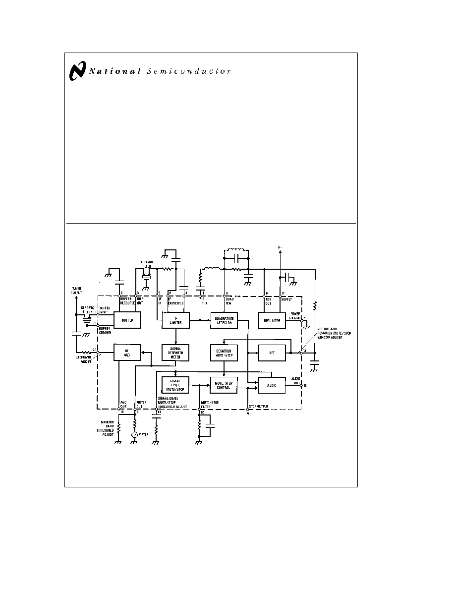
Block Diagram
Order Number LM1865M
or LM1865N
See NS Package Number
M20B or N20A
TL H 7509 1
FIGURE 1
C1995 National Semiconductor Corporation
RRD-B30M115 Printed in U S A
Absolute Maximum Ratings
If Military Aerospace specified devices are required
please contact the National Semiconductor Sales
Office Distributors for availability and specifications
Supply Voltage Pin 17
16V
Package Dissipation (Note 1)
2 0W
Storage Temperature Range
b
55 C to
a
150 C
Operating Temperature Range
b
20 C to
a
85 C
Max Voltage on Pin 16 (Stop Output)
16V
Soldering Information
Dual-In-Line Package
Soldering (10 seconds)
260 C
Small Outline Package
Vapor Phase (60 seconds)
215 C
Infrared (15 seconds)
220 C
See AN-450 ``Surface Mounting Methods and Their Effect
on Product Reliability'' for other methods of soldering sur-
face mount devices
Electrical Characteristics
Test Circuit T
A
e
25 C V
a
e
12V S1 in position 2 S2 in position 1 and S3 in position 2 unless indicated otherwise
Parameter
Conditions
Min
Typ
Max
Units
STATIC CHARACTERISTICS
Supply Current
33
45
mA
Pin 9 Regulator Voltage
5 7
V
Operating Voltage Range
(See Note 2)
7 3
16
V
Pin 18 Output Leakage Current
Pin 20 Open V
IF
e
0 S3 in Position 1
0 1
m
A
Pin 16 Stop Low Output Voltage
S1 in Position 1 S2 in Position 3
0 3
V
Pin 16 Stop High Output Leakage Current
S2 in Position 2 V14
e
V9
0 1
m
A
Pin 15 Audio Output Resistance
4 7
kX
Pin 1 Buffer Input Resistance
Measured at DC
350
X
Pin 3 Buffer Output Resistance
Measured at DC
350
X
Pin 20 Wide Band Input Resistance
Measured at DC
2
X
Pin 8 Meter Output Resistance
1
kX
DYNAMIC CHARACTERISTICS
f
MOD
e
400 Hz f
o
e
10 7 MHz Deviation
e
g
75 kHz
b
3 dB Limiting Sensitivity
IF Only (See Note 3)
60
120
m
Vrms
Buffer Voltage Gain
V
IN
Pin 1
e
10 mVrms at 10 7 MHz
19
22
25
dB
Recovered Audio
V
IF
e
10 mVrms V14
e
V9
275
320
470
mVrms
Signal-to-Noise
V
IF
e
10 mVrms V14
e
V9 (See Note 4)
70
84
dB
AM Rejection
V14
e
V9
V
IF
e
1 mV 30% AM Mod
50
60
dB
V
IF
e
10 mV 30% AM Mod
50
60
dB
Minimum Total Harmonic Distortion
V
IF
e
10 mV
0 1
0 35
%
THD at Frequency where V14
e
V9
V
IF
e
10 mV Tune until V14
e
V9
0 1
0 45
%
(Zero AFT Offset)
THD
g
10 kHz from Frequency where V14
e
V9
V
IF
e
10 mV
0 15
%
AFT Offset Frequency for Low
V
IF
e
10 mV S2 in Position 3 f
MOD
e
0
g
50
kHz
Stop Output at Pin 16
Offset
e
(Frequency for Pin 16 Low)
b
(Frequency where V14
e
V9)
Ultrasonic Mute Stop Level Threshold
V14
e
V9 S1 in Position 3 (See Note 5)
60
kHz
V
IF
e
10 mV
f
MOD
e
100 kHz
S2 in Position 3
Amount of Deviation where V16
x
Low
2
Electrical Characteristics
Test Circuit T
A
e
25 C V
a
e
12V S1 in position 2 S2 in position 1 and S3 in
position 2 unless indicated otherwise (Continued)
Parameter
Conditions
Min
Typ
Max
Units
DYNAMIC CHARACTERISTICS
f
MOD
e
400 Hz f
o
e
10 7 MHz Deviation
e
g
75 kHz (Continued)
Pin 13 Mute Stop Threshold Voltage
V14
e
V9 S1 in Position 4
220
mV
S2 in Position 3
V13 where V16
x
Low
Amount of Muting (LM1965 Only)
S2 in Position 4 S1 in Position 1 V
IF
e
10 mV
66
dB
Amount of Muting with Pin 13 and
S1 in Position 1
0
dB
Pin 16 Grounded
V14
e
V9 V
IF
e
10 mV
Narrow Band AGC Threshold
Increase IF Input until I
AGC
e
0 1 mA
100
210
300
m
Vrms
Pin 20
e
30 mVrms
Wide Band AGC Threshold
V
IF
e
100 mVrms
5
12
22
mVrms
Increase Signal to Pin 20 until I
AGC
e
0 1 mA
Pin 18 Low Output Voltage
V
IN
Pin 20
e
100 mV V
IF
e
100 mVrms
0 2
0 5
V
(LM1865 and LM1965 only)
Pin 18 High Output Voltage (LM2065 only)
V
IN
Pin 20
e
100 mV V
IF
e
100 mVrms (See Note 6)
11 7
V
Pin 8 Meter Output Voltage
V
IF
e
10 mV
0 1
V
V
IF
e
300 mV
1 1
V
V
IF
e
3 mV
2 6
V
Note 1
Above T
A
e
25 C derate based on T
J(max)
e
150 C and i
JA
e
60 C W
Note 2
All data sheet specifications are for V
a
e
12V may change slightly with supply
Note 3
When the IF is preceded by 22 dB gain in the buffer excellent system sensitivity is achieved
Note 4
Measured with a notch at 60 Hz and 20 Hz to 100 kHz bandwidth
Note 5
FM modulate RF source with a 100 kHz audio signal and find what modulation level expressed as kHz deviation results in V16
x
12V
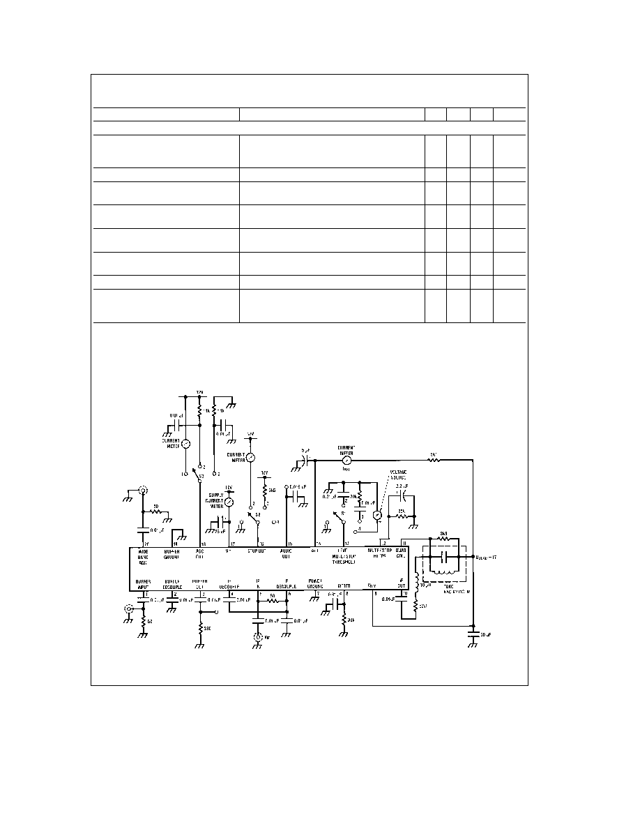
Test Circuit
TL H 7509 2
FIGURE 2
3
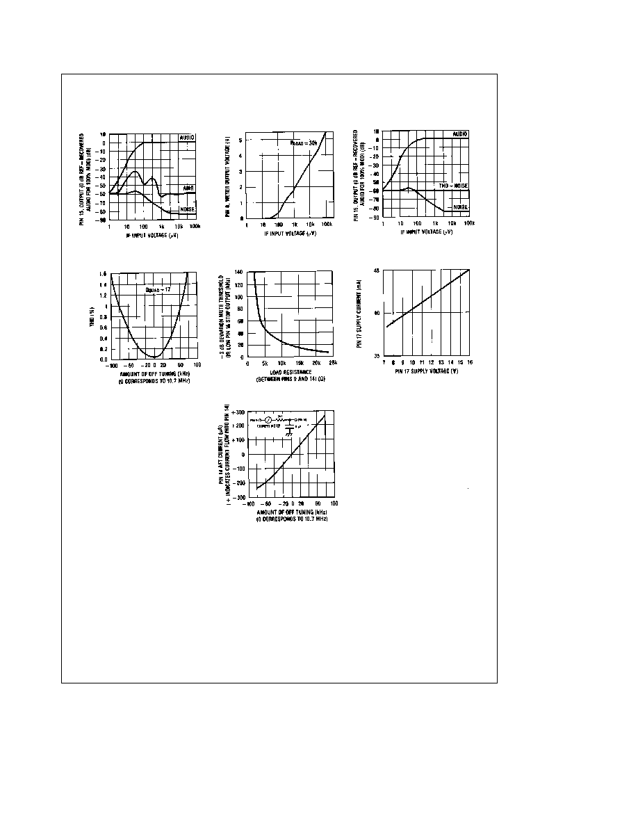
Typical Performance Characteristics
(from Test Circuit)
FM Limiting Characteristics
and AM Rejection
Pin 8 Meter Output Voltage
vs IF Input Level
FM Limiting Characteristics
a
THD
% THD vs OFF Tuning
(Single Tuned Quadrature
Coil)
Deviation Mute Stop
Threshold as a Function of
AFT Load Resistor
Supply Current vs
Supply Voltage
Pin 14 AFT Current
vs Tuning
TL H 7509 3
Coils and ceramic filters are available from
Toko America
1250 Feehanville Drive
Mount Prospect IL 60056
(312) 297-0070
Murata
2200 Lake Park Drive
Smyrna GA 30080
(404) 436-1300
4
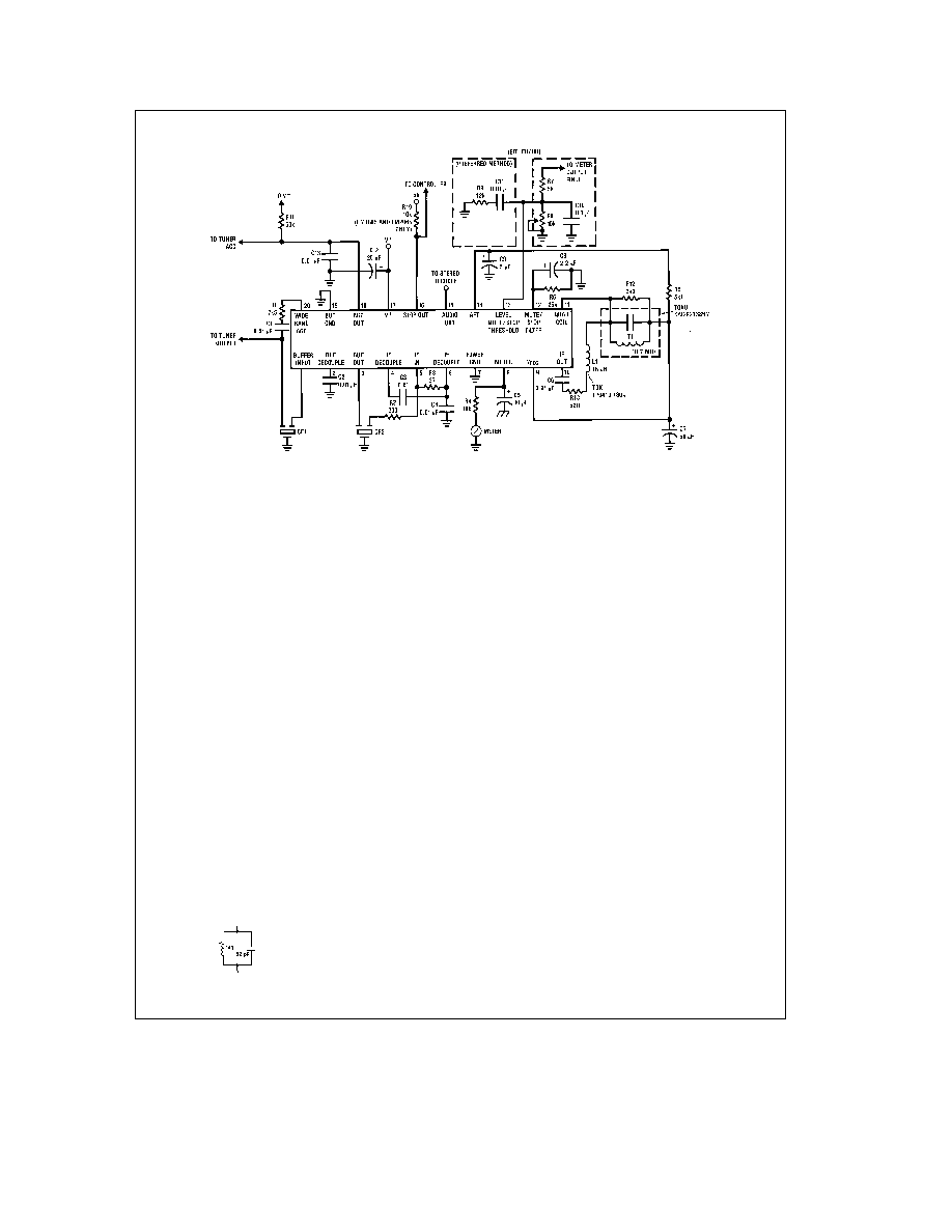
Application Circuit
TL H 7509 4
FIGURE 3
IC External Components
(See Application Circuit)
Component
Typical Value
Comments
C1
0 01 mF
AC coupling for wide band AGC input
C2
0 01 mF
Buffer and AGC supply decoupling
C3 C4
0 01 mF
IF decoupling capacitors
C5
10 mF
Meter decoupling capacitor
C6
0 01 mF
AC coupling for IF output
C7
50 mF
Regulator decoupling capacitor affects S N floor
C8
2 2 mF
Level mute stop time constant
C9
5 mF
AFT decoupling affects stop time
C10
0 1 mF
Disables noise mute stop
C11
0 01 mF
AC coupling for noise mute stop threshold adjust
C12
25 mF
Supply decoupling
C13
0 01 mF
AGC output decoupling capacitor
R1
Tuner Dependent
Wide band AGC threshold adjust
R2 R3
Tuner Dependent
Gain set and bias for IF R2
a
R3
e
330X to terminate ceramic filter
R4
Meter Dependent
Sets full-scale on meter
R5
5k1
Deviation mute stop window adjustment
R6
25k
Mute stop filter affects stop time
R7
5k
Level mute stop threshold adjustment
R8
10k Pot
Level mute stop threshold adjustment
R9
12k
Noise mute stop threshold adjustment decrease resistor for lower
S N at threshold for optimum performance over temp and gain varia-
tion set this resistor value so that the signal level mute stop threshold
occurs in the radio at 45dB S N (
g
3 dB) in mono
R10
10k
Load for open-collector stop output
R11
50k
AGC output load resistor for open-collector output
R12
3k9
Sets Q of quadrature coil affecting THD S N and recovered audio
R13
62X
Optimises minimum THD
L1
18 mH Q
u
l
50
10 7 MHz
Sets signal swing across quadrature coil High Q is important to mini-
TDK Electronics
mize effect variation of Q has on both minimum THD and AFT offset
TPO410-180K or equivalent
T1
Q
u
l
70
10 7 MHz L to
10 7 MHz quadrature coil Q
UL
l
70
resonate w 82 pF
10 7 MHz
TOKO KAC-K2318HM or
equivalent
CF1 CF2
10 7 MHz ceramic resonators provide selectivity good group delay
Murata SFE10 7ML or equivalent
characteristics important for low THD of system
TL H 7509 5
5