 | –≠–ª–µ–∫—Ç—Ä–æ–Ω–Ω—ã–π –∫–æ–º–ø–æ–Ω–µ–Ω—Ç: LM1893 | –°–∫–∞—á–∞—Ç—å:  PDF PDF  ZIP ZIP |

TL H 6750
LM1893LM2893
Carrier-Current
Transceiver
April 1995
LM1893 LM2893 Carrier-Current Transceiver
General Description
Carrier-current systems use the power mains to transfer in-
formation between remote locations This bipolar carrier-
current chip performs as a power line interface for half-du-
plex (bi-directional) communication of serial bit streams of
virtually any coding In transmission a sinusoidal carrier is
FSK modulated and impressed on most any power line via a
rugged on-chip driver In reception a PLL-based demodula-
tor and impulse noise filter combine to give maximum range
A complete system may consist of the LM1893 a COPS
TM
controller and discrete components
Features
Y
Noise resistant FSK modulation
Y
User-selected impulse noise filtering
Y
Up to 4 8 kBaud data transmission rate
Y
Strings of 0's or 1's in data allowed
Y
Sinusoidal line drive for low RFI
Y
Output power easily boosted 10-fold
Y
50 to 300 kHz carrier frequency choice
Y
TTL and MOS compatible digital levels
Y
Regulated voltage to power logic
Y
Drives all conventional power lines
Applications
Y
Energy management systems
Y
Home convenience control
Y
Inter-office communication
Y
Appliance control
Y
Fire alarm systems
Y
Security systems
Y
Telemetry
Y
Computer terminal interface
Typical Application
TL H 6750 ≠ 1
FIGURE 1 Block diagram of carrier
current chip with a complement of discrete components making a complete
F
O
e
125 kHz f
DATA
e
360 Baud transceiver Use caution with this circuit
dangerous line voltage is present
BI-LINE
TM
and COPS
TM
are trademarks of National Semiconductor Corp
Carrier-Current Transceivers are also called Power Line Carrier (PLC) transceivers
C1995 National Semiconductor Corporation
RRD-B30M115 Printed in U S A
Absolute Maximum Ratings
If Military Aerospace specified devices are required
please contact the National Semiconductor Sales
Office Distributors for availability and specifications
Supply voltage
30 V
Voltage on pin 12
55 V
Voltage on pin 10 (Note 1)
41 V
Voltage on pins 5 and 17
40 V
5 6 V DC zener current
100 mA
Junction temperature
transmit mode
150 C
receive mode
125 C
Electro-Static Discharge (120 pF 1500X)
1KV
Maximum continuous dissipation T
A
e
25 C
plastic DIP N (Note 2)
transmit mode
1 66 W
receive mode
1 33 W
Operating ambient temp range
b
40 to 85 C
Storage temperature range
b
65 to 150 C
Lead temp soldering 7 seconds
260 C
Note
Absolute maximum ratings indicate limits beyond
which damage to the device may occur Electrical specifica-
tions are not ensured when operating the device above
guaranteed limits but below absolute maximum limits but
there will be no device degradation
General Electrical Characteristics
(Note 3) The test conditions are V
a
e
18V and F
O
e
125 kHz unless otherwise noted
Test
Design
Limit
Parameter
Conditions
Typical
Limit
Limit
Units
(Note 4)
(Note 5)
1
5 6 V Zener voltage V
Z
Pin 11 I
Z
e
2 mA
5 6
5 2
V min
5 9
V max
2
5 6 V Zener resistance R
Z
Pin 11 R
Z
e
(V
Z
10 mAbV
Z
1 mA) (10 mAb1 mA)
5
X
3
Carrier I O peak survivable
Pin 10 discharge 1 mF cap charged to V
OT
80
60
V max
transient voltage V
OT
thru
k
1X
4
Carrier I O clamp voltage V
OC
Pin 10 I
OC
e
10 mA RX mode
44
41
V min
2N2222 diode pin 8 to 9
50
V max
5
Carrier I O clamp resistance R
10
Pin 10 I
OC
e
10 mA
20
X
6
TX RX low input voltage V
IL
Pin 5
1 8
0 8
V max
7
TX RX high input voltage V
IH
Pin 5 (Note 9)
2 2
2 8
V min
8
TX RX low input current I
IL
Pin 5 at 0 8 V
b
2
b
20
m
A min
1
m
A max
9
TX RX high input current I
IH
Pin 5 at 40 V
b
1
0
m
A min
10
b
4
10
m
A max
10
RXbTX switch-over time T
RT
Time to develop 63% of full current drive thru pin 10
10
m
s
11
TXbRX switch-over time T
TR
1 bit time T
B
e
1 (2F
DATA
) Time T
TR
is user
2
bit
controlled with C
M
see Apps Info
12
ICO initial accuracy of F
O
TX mode R
O
e
6 65 kX C
O
e
560 pF
125
113
kHz min
F
0
e
(F
1
a
F
2
) 2
137
kHz max
13
ICO temperature coefficient of F
O
TX or RX mode (F
OMAX
b
F
OMIN
) (T
JMAX
b
T
JMIN
)
b
100
PPM C
14
Temperature drift of F
O
TX or RX mode b40
s
T
J
s
T
JMAX
g
2 0
g
5 0
% max
Transmitter Electrical Characteristics
(Note 3) The test conditions are V
a
e
18 V and F
O
e
125 kHz
unless otherwise noted The transmit center frequency is F
O
FSK low is F
1
and FSK high is F
2
Test
Design
Limit
Parameter
Conditions
Typical
Limit
Limit
Units
(Note 4)
(Note 5)
15
Supply voltage V
a
range
Meets test 17 spec at T
J
e
25 C and
13
14
15
V min
l
(F
1
14V bF
1
18V ) F
1
18V
l
k
0 01
40
24
23
V max
l
(F
1
24V bF
1
18V ) F
1
18V
l
k
0 01
16
Total supply current I
QT
Pin 15 Pin 12 high I
QT
is I
Q
through
52
79
mA max
pin 15 and the average current I
ODC
of the
Carrier I O through pin 10
17
Carrier I O output current I
O
100X load on pin 10
70
45
mApp min
18
Carrier I O lower swing limit V
ALC
Pin 10 Set internally be ALC
4 7
4 0
V min
2N2222 diode pin 8 to 9
5 7
V max
19
THD of I
O
(Note 6)
Q of 10 tank driving 10X line
0 6
5 0
% max
100X load no tank
5 5
9
% max
20
FSK deviation F
2
b
F
1
(F
2
b
F
1
) ( F
2
a
F
1
2)
4 4
3 7
% min
5 2
% max
21
Data In low input voltage V
IL
Pin 17
1 7
0 8
V max
22
Data In high input voltage V
IH
Pin 17 (Note 9)
2 1
2 8
V min
23
Data In low input current I
IL
Pin 17 at 0 8 V
b
1
b
10
m
A min
1
m
A max
24
Data In high input current I
IH
Pin 17 at 40 V
b
1
0
m
A min
10
b
4
10
m
A max
2
Receiver Electrical Characteristics
(Note 3) The test conditions are V
a
e
18 V F
O
e
125 kHz
g
2 2%
deviation FSK F
DATA
e
2 4 kHz V
IN
e
100 mVpp in the receive mode unless otherwise noted
Test
Design
Limit
Parameter
Conditions
Typical
Limit
Limit
Units
(Note 4)
(Note 5)
25
Supply voltage V
a
range
Functional receiver (Note 7)
12
13
13 5
V min
37
30
28
V max
26
Supply current I
QT
I
QT
is pin 15 (V
a
) plus pin 10
11
5
mA min
(Carrier I O) current 2 4 kX Pin 13 to GND
14
mA max
27
Carrier I O input resistance R
10
Pin 10
19 5
14
kX min
30
kX max
28
Max data rate F
MD
Functional receiver (Note 7) C
F
e
100 pF
10
4 8
2 4
kBaud
R
F
e
0X no tank
2 4 kHze4 8 kBaud
29
PLL capture range F
C
C
F
e
100 pF R
F
e
0 X
g
40
g
15
g
10
% min
30
PLL lock range F
L
C
F
e
100 pF R
F
e
0 X
g
45
g
15
% min
31
Receiver input sensitivity S
IN
For a functional receiver (Note 8)
Referred to chip side (pin 10)
1 8
10
12
mV
RMS
of the line-coupling XFMR F
O
e
50 kHz
2 0
mV
RMS
F
O
e
300 kHz
1 4
mV
RMS
Referred to line side of XFMR
0 26
mV
RMS
(assuming a 7 07 1 XFMR) F
O
e
50 kHz
0 29
mV
RMS
F
O
e
300 kHz
0 20
mV
RMS
32
Tolerable input dc voltage offset
Pin 10 lower than pin 15 by V
INDC
2
0 1
V max
range V
INDC
33
Data Out breakdown voltage
Pin 12 leakage I
s
20 mA
70
55
V min
34
Data Out low output V
OL
Pin 12 sat voltage at I
OL
e
2 mA
0 15
0 4
V max
35
Impulse noise filter current I
I
Pin 13 charge and discharge current
g
55
g
45
m
A min
g
85
m
A max
36
Offset hold cap bias voltage V
CM
Pin 6
2 0
1 3
V min
3 5
V max
37
Offset hold capacitor max drive
Pin 6 V(pin 3)bV(pin 4)e
g
250 mV
g
55
g
25
m
A min
current I
MCM
g
80
m
A max
38
Offset hold bias current I
OHB
Pin 6 TX mode Bias pin 6 as it self-
b
0 5
b
20
b
40
nA min
biased during test 31
40
nA max
39
Phase comparator current I
PC
Bias pins 3 and 4 at 8 5 V
100
50
m
A min
I
PC
e
I(pin 3) a I(pin 4) TX mode
200
m
A max
40
Phase detector output resistance
Pins 3 and 4
10
6
kX min
R
PD
R
PD
e
(V 100mAbV 50mA) (50mA)
18
kX max
41
Phase detector demodulated output
Pin 3 to 4 measured after filtering
100
60
mVpp min
voltage V
PD
out the 2F
O
component
180
mVpp max
42
Fast offset cancel voltage ``window''
V
PIN3
b
V
PIN4
e
g
V
WINDOW
a
DC offset
0 95
0 70
V V min
-to-V
PD
ratio V
W
V
PD
Drive for
g
1 mA pin 6 current
1 20
V V max
43
Power supply rejection PSRR
C
L
e
0 1 mF PSRR e CMRR 120 Hz
80
dB min
Note 1
More accurately the maximum voltage allowed on pin 10 is V
OC
and V
OC
ranges from 41 to 50V Also transients may reach above 60V see the transient
peak voltage characteristic curve
Note 2
The maximum power dissipation rating should be derated for device operation above 25 C to insure that the junction temperature remains below the
maximum rating Use a i
JA
of 75 C W for the N package using a socket in still air (which is the worst case) Consult the Application Information section for more
detail
Note 3
The boldface values apply over the full junction temperature range for the specified supply voltage range All other numbers apply at T
A
e
T
J
e
25 C Pin
numbers refer to LM1893 LM2893 tested by shorting Carrier In to Carrier Out and testing it as an LM1893
Note 4
Guaranteed and 100% production tested
Note 5
Guaranteed (but not 100% production tested) over the temperature and supply voltage ranges These limits are not used to calculate outgoing quality
levels
Note 6
Total harmonic distortion is measured using THD
e
I
RMS
(all components at or above 2F
O
)
I
RMS
(fundamental)
Note 7
Receiver function is defined as the error-free passage of 1 cycle of 50% duty-cycle 2 4 kHz square-wave data (2 sequential 208 mS bits) with the first bit
being a ``1 '' All of the data transitions (edges) must fall within
g
10% (
g
20 8 ms) of their noise-free positions RX time delay is minimized by using no impulse noise
filter cap C
I
for this test
Note 8
During the sensitivity check note 7 requirements are followed with these exceptions (1) data rate F
DATA
e
1 2 kHz (2) all of the data transitions must fall
within
g
20% (
g
41 6 ms) of their noise-free positions and (3) a time-domain filter capacitor (C
I
) is used The time delay of C
I
is
bit or 208 ms (C
I
is
approximately 6200 pF)
Note 9
For TTL compatibility use a pull-up resistor to increase min V
OH
to above 2 8 V
3
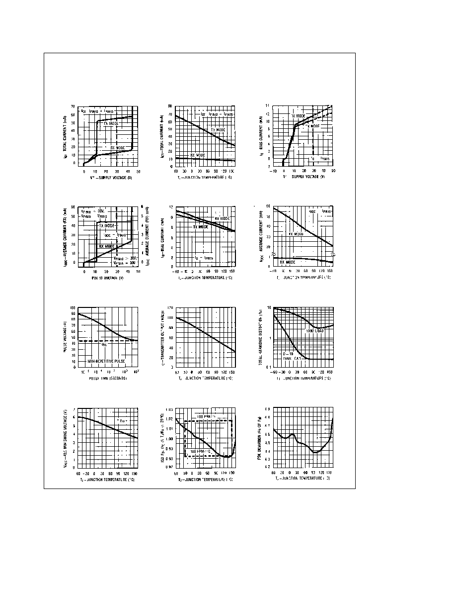
Typical Performance Characteristics
(V
a
e
18V F
O
e
125 kHz circuit of
Figure 1 pin numbers for
LM1893)
Total Current Consumption
I
QT
vs Supply Voltage
Total Current Consumption
I
QT
vs Junction Temperature
Chip Bias Current
i
Q
vs Supply Voltage
Chip Bias Current I
Q
vs Junction Tempurature
Output Stage DC Current
I
ODC
vs Output Voltage
Output Stage DC Current
I
ODC
vs
Junction Temperature
Transient Voltage Survival
vs Pulse Time
Transmitter AC Output Current
vs Junction Temperature
Transmitter Sinusoid THD
vs Junction Temperature
ALC Voltage vs
Junction Temperature
ICO Frequency vs
Junction Temperature
Transmitter FSK Deviation
vs Junction Temperature
TL H 6750 ≠ 38
4
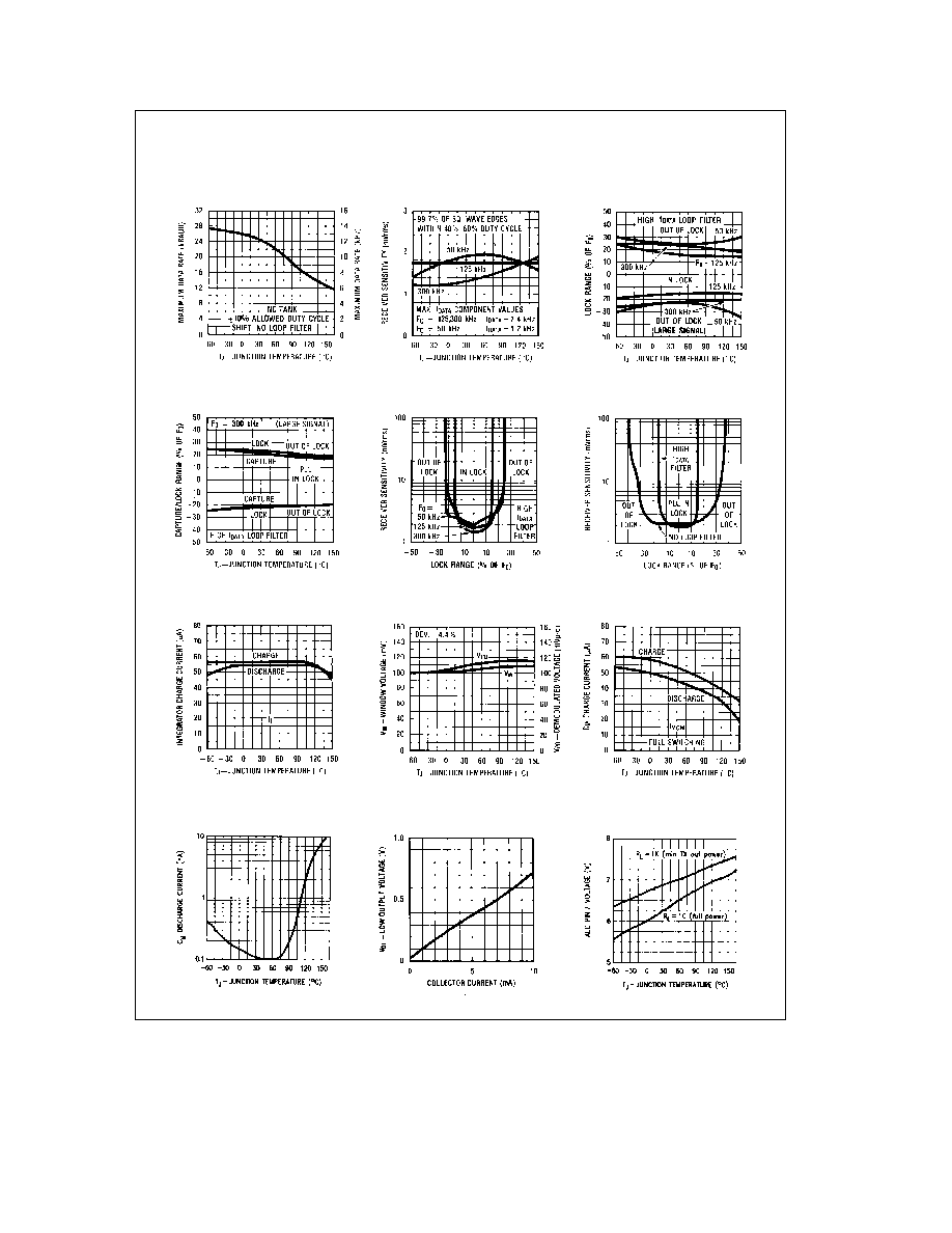
Typical Performance Characteristics
(Continued)
Maximum Data Rate vs
Junction Temperature
Receiver Sensitivity vs
Junction Temperature
PLL Lock Range vs
Junction Temperature and F
O
PLL Capture
Lock Range vs
Junction Temperature
Receiver Sensitivity vs
PLL Lock Range and F
O
Receiver Sensitivity vs
PLL Lock Range and Loop Filter
Impulse Noise Filter
Current vs Junction
Temperature
Phase Detector Output
Voltage vs Junction
Temperature
Offset Hold Cap Charge
Currents vs Junction
Temperature
Offset Hold Cap Bias Current vs
Junction Temperature
Data Out Low Voltage vs
Pull Down Current
Pin 7 Bias Voltage vs
Junction Temperature
TL H 6750 ≠ 39
5