 | –≠–ª–µ–∫—Ç—Ä–æ–Ω–Ω—ã–π –∫–æ–º–ø–æ–Ω–µ–Ω—Ç: LM1894MTX | –°–∫–∞—á–∞—Ç—å:  PDF PDF  ZIP ZIP |
LM1894
Dynamic Noise Reduction System DNR
Æ
General Description
The LM1894 is a stereo noise reduction circuit for use with
audio
playback
systems.
The
DNR
system
is
non-complementary, meaning it does not require encoded
source material. The system is compatible with virtually all
prerecorded tapes and FM broadcasts. Psychoacoustic
masking, and an adaptive bandwidth scheme allow the DNR
to achieve 10 dB of noise reduction. DNR can save circuit
board space and cost because of the few additional compo-
nents required.
Features
n
Non-complementary noise reduction, "single ended"
n
Low cost external components, no critical matching
n
Compatible with all prerecorded tapes and FM
n
10 dB effective tape noise reduction CCIR/ARM
weighted
n
Wide supply range, 4.5V to 18V
n
1 Vrms input overload
Applications
n
Automotive radio/tape players
n
Compact portable tape players
n
Quality HI-FI tape systems
n
VCR playback noise reduction
n
Video disc playback noise reduction
Typical Application
DNR
Æ
is a registered trademark of National Semiconductor Corporation.
The DNR
Æ
system is licensed to National Semiconductor Corporation under U.S. patent 3,678,416 and 3,753,159.
Trademark and license agreement required for use of this product.
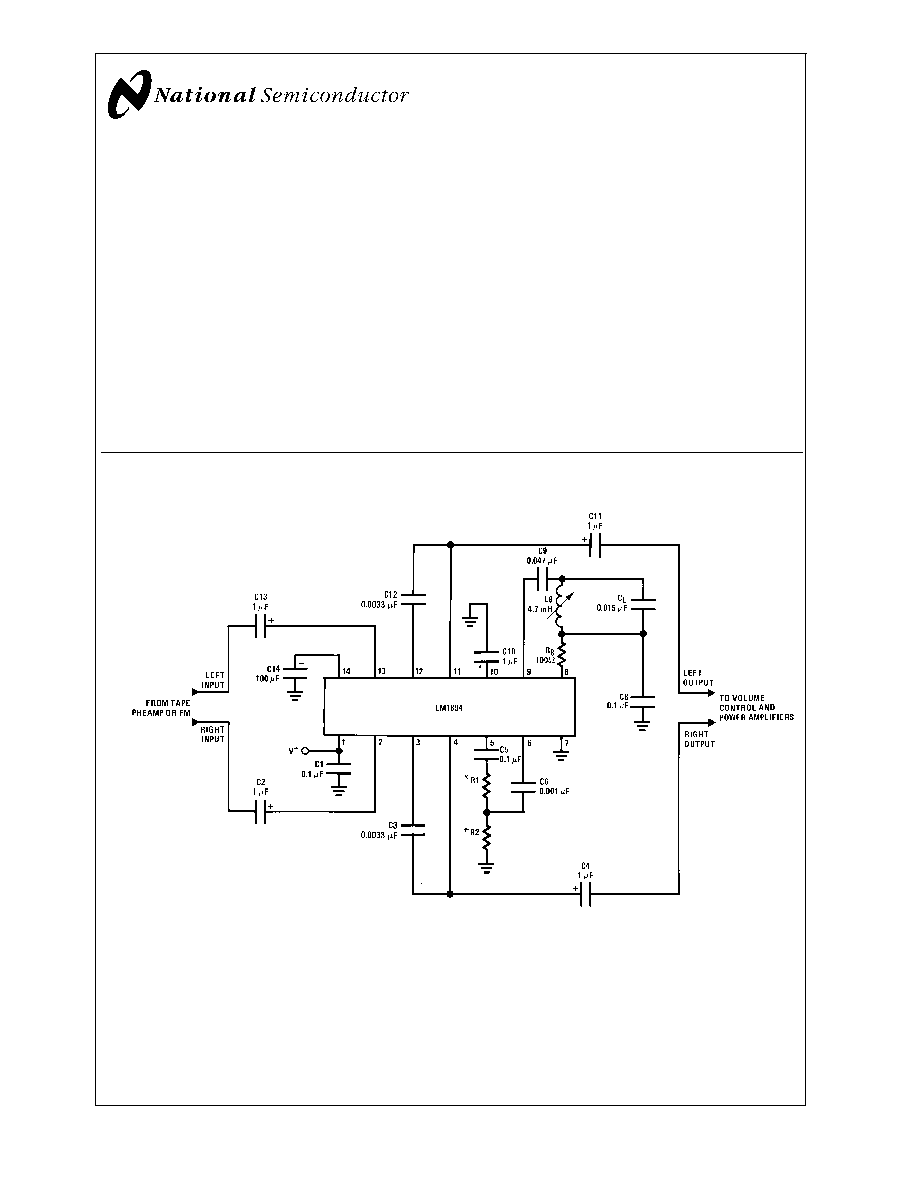
DS007918-1
*R1 + R2 = 1 k
total.
See Application Hints.
Order Number LM1894M, LM1894N, or LM1894MT
See NS Package Number M14A, N14A, or MTC14
FIGURE 1. Component Hook-Up for Stereo DNR System
April 2002
LM1894
Dynamic
Noise
Reduction
System
DNR
© 2002 National Semiconductor Corporation
DS007918
www.national.com

Absolute Maximum Ratings
(Note 1)
If Military/Aerospace specified devices are required,
please contact the National Semiconductor Sales Office/
Distributors for availability and specifications.
Supply Voltage
20V
Input Voltage Range, V
pk
V
S
/2
Operating Temperature (Note 2)
0∞C to +70∞C
Storage Temperature
-65∞C to +150∞C
Soldering Information
Dual-In-Line Package
Soldering (10 seconds)
260∞C
Small Outline Package
Vapor Phase (60 seconds)
215∞C
Infrared (15 seconds)
220∞C
See AN-450 "Surface Mounting Methods and Their Effect
on Product Reliability" for other methods of soldering
surface mount devices.
Note 1: "Absolute Maximum Ratings" indicate limits beyond which damage
to the device may occur. Operating Ratings indicate conditions for which the
device is functional, but do not guarantee specific performance limits.
Electrical Characteristics
V
S
= 8V, T
A
= 25∞C, V
IN
= 300 mV at 1 kHz, circuit shown in
Figure 1 unless otherwise specified
Parameter
Conditions
Min
Typ
Max
Units
Operating Supply Range
4.5
8
18
V
Supply Current
V
S
= 8V
17
30
mA
MAIN SIGNAL PATH
Voltage Gain
DC Ground Pin 9, (Note 3)
-0.9
-1
-1.1
V/V
DC Output Voltage
3.7
4.0
4.3
V
Channel Balance
DC Ground Pin 9
-1.0
1.0
dB
Minimum Balance
AC Ground Pin 9 with 0.1 µF
675
965
1400
Hz
Capacitor, (Note 3)
Maximum Bandwidth
DC Ground Pin 9, (Note 3)
27
34
46
kHz
Effective Noise Reduction
CCIR/ARM Weighted, (Note 4)
-10
-14
dB
Total Harmonic Distortion
DC Ground Pin 9
0.05
0.1
%
Input Headroom
Maximum V
IN
for 3% THD
1.0
Vrms
AC Ground Pin 9
Output Headroom
Maximum V
OUT
for 3% THD
V
S
- 1.5
Vp-p
DC Ground Pin 9
Signal to Noise
BW = 20 Hz≠20 kHz, re 300 mV
AC Ground Pin 9
79
dB
DC Ground Pin 9
77
dB
CCIR/ARM Weighted re 300 mV
(Note 5)
AC Ground Pin 9
82
88
dB
DC Ground Pin 9
70
76
dB
CCIR Peak, re 300 mV, (Note 6)
AC Ground Pin 9
77
dB
DC Ground Pin 9
64
dB
Input Impedance
Pin 2 and Pin 13
14
20
26
k
Channel Separation
DC Ground Pin 9
-50
-70
dB
Power Supply Rejection
C14 = 100 µF,
V
RIPPLE
= 500 mVrms,
-40
-56
dB
f = 1 kHz
Output DC Shift
Reference DVM to Pin 14 and
Measuree Output DC Shift from
4.0
20
mV
Minimum to Maximum Band-
width, (Note 7).
CONTROL SIGNAL PATH
Summing Amplifier Voltage Gain
Both Channels Driven
0.9
1
1.1
V/V
Gain Amplifier Input Impedance
Voltage Gain
Pin 6
24
30
39
k
Pin 6 to Pin 8
21.5
24
26.5
V/V
LM1894
www.national.com
2
Electrical Characteristics
(Continued)
V
S
= 8V, T
A
= 25∞C, V
IN
= 300 mV at 1 kHz, circuit shown in
Figure 1 unless otherwise specified
Parameter
Conditions
Min
Typ
Max
Units
CONTROL SIGNAL PATH
Peak Detector Input Impedance
Pin 9
560
700
840
Voltage Gain
Pin 9 to Pin 10
30
33
36
V/V
Attack Time
Measured to 90% of Final Value
300
500
700
µs
with 10 kHz Tone Burst
Decay Time
Measured to 90% of Final Value
45
60
75
ms
with 10 kHz Tone Burst
DC Voltage Range
Minimum Bandwidth to Maximum
1.1
3.8
V
Bandwidth
Note 2: For operation in ambient temperature above 25∞C, the device must be derated based on a 150∞C maximum junction temperature and a thermal resistance
of 1) 80∞C/W junction to ambient for the dual-in-line package, 2) 105∞C/W junction to ambient for the small outline package, and 3) 150∞C/W junction to ambient for
the TSSOP package.
Note 3: To force the DNR system into maximum bandwidth, DC ground the input to the peak detector, pin 9. A negative temperature coefficient of -0.5%/∞C on the
bandwidth, reduces the maximum bandwidth at increased ambient temperature or higher package dissipation. AC ground pin 9 or pin 6 to select minimum
bandwidth. To change minimum and maximum bandwidth, see Appliction Hints.
Note 4: The maximum noise reduction CCIR/ARM weighted is about 14 dB. This is accomplished by changing the bandwidth from maximum to minimum. In actual
operation, minimum bandwidth is not selected, a nominal minimum bandwidth of about 2 kHz gives -10 dB of noise reduction. See Application Hints.
Note 5: The CCIR/ARM weighted noise is measured with a 40 dB gain amplifier between the DNR system and the CCIR weighting filter; it is then input referred.
Note 6: Measured using the Rhode-Schwartz psophometer.
Note 7: Pin 10 is DC forced half way between the maximum bandwidth DC level and minimum bandwidth DC level. An AC 1 kHz signal is then applied to pin 10.
Its peak-to-peak amplitude is V
DC
(max BW) - V
DC
(min BW).
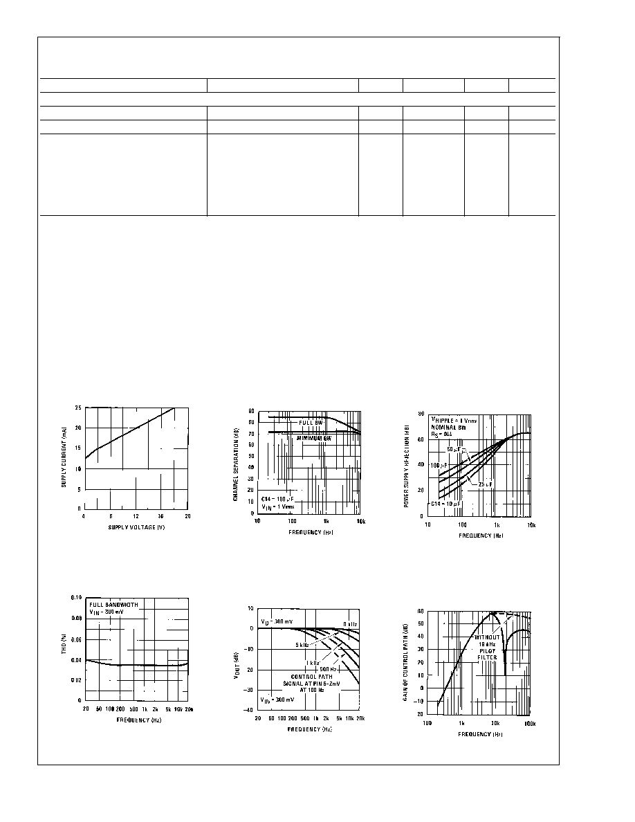
Typical Performance Characteristics
Supply Current vs
Supply Voltage
DS007918-13
Channel Separation
(Referred to the Output)
vs Frequency
DS007918-14
Power Supply Rejection
Ratio (Referred to the
Output) vs Frequency
DS007918-15
THD vs Frequency
DS007918-16
-3 dB Bandwidth
vs Frequency and
Control Signal
DS007918-17
Gain of Control Path
vs Frequency (with
10 kHz FM Pilot Filter)
DS007918-18
LM1894
www.national.com
3

Typical Performance Characteristics
(Continued)
Main Signal Path
Bandwidth vs
Voltage Control
DS007918-3
Peak Detector Response
DS007918-4
Output Response
DS007918-5
LM1894
www.national.com
4
External Component Guide
(
Figure 1)
Component
Value
Purpose
C1
0.1 µF≠
100 µF
May be part of power supply,
or may be added to suppress
power supply oscillation.
C2, C13
1 µF
Blocks DC, pin 2 and pin 13
are at DC potential of V
S
/2.
C2, C13 form a low frequency
pole with 20k R
IN
.
C14
25 µF≠
100 µF
Improves power supply
rejection.
C3, C12
0.0033 µF
Forms integrator with internal
gm block and op amp. Sets
bandwidth conversion gain of
33 Hz/µA of gm current.
C4, C11
1 µF
Output coupling capacitor.
Output is at DC potential of
V
S
/2.
C5
0.1 µF
Works with R1 and R2 to
attenuate low frequency
transients which could disturb
control path operation.
C6
0.001 µF
Works with input resistance of
pin 6 to form part of control
path frequency weighting.
C8
0.1 µF
Combined with L8 and C
L
forms 19 kHz filter for FM
pilot. This is only required in
FM applications (Note 9).
L8, C
L
4.7 mH,
0.015 µF
Forms 19 kHz filter for FM
pilot. L8 is Toko coil
CAN-1A185HM (Notes 8, 9).
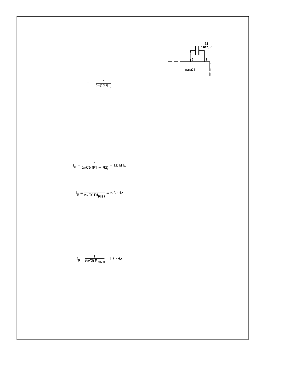
C9
0.047 µF
Works with input resistance of
pin 9 to form part of control
path frequency weighting.
C10
1 µF
Set attack and decay time of
peak detector.
R1, R2
1 k
Sensitivity resistors set the
noise threshold. Reducing
attentuation causes larger
signals to be peak detected
and larger bandwidth in main
signal path. Total value of R1
+ R2 should equal 1 k
.
R8
100
Forms RC roll-off with C8.
This is only required in FM
applications.
Note 8: Toko America Inc., 1250 Feehanville Drive, Mt. Prospect IL 60056
Note 9: When FM applications are not required, pin 8 and pin 9 hook-up as
follows:
Circuit Operation
The LM1894 has two signal paths, a main signal path and a
bandwidth control path. The main path is an audio low pass
filter comprised of a gm block with a variable current, and an
op amp configured as an integrator. As seen in
Figure 2, DC
feedback constrains the low frequency gain to A
V
= -1.
Above the cutoff frequency of the filter, the output decreases
at -6 dB/oct due to the action of the 0.0033 µF capacitor.
The purpose of the control paths is to generate a bandwidth
control signal which replicates the ear's sensitivity to noise in
the presence of a tone. A single control path is used for both
channels to keep the stereo image from wandering. This is
done by adding the right and left channels together in the
summing amplifier of
Figure 2. The R1, R2 resistor divider
adjusts the incoming noise level to open slightly the band-
width of the low pass filter. Control path gain is about 60 dB
and is set by the gain amplifier and peak detector gain. This
large gain is needed to ensure the low pass filter bandwidth
can be opened by very low noise floors. The capacitors
between the summing amplifier output and the peak detector
input determine the frequency weighting as shown in the
typical performance curves. The 1 µF capacitor at pin 10, in
conjunction with internal resistors, sets the attack and decay
times. The voltage is converted into a proportional current
which is fed into the gm blocks. The bandwidth sensitivity to
gm current is 33 Hz/µA. In FM stereo applications at 19 kHz
pilot filter is inserted between pin 8 and pin 9 as shown in
Figure 1.
Figure 3 is an interesting curve and deserves some discus-
sion. Although the output of the DNR system is a linear
function of input signal, the -3 dB bandwidth is not. This is
due to the non-linear nature of the control path. The DNR
system has a uniform frequency response, but looking at the
-3 dB bandwidth on a steady state basis with a single
frequency input can be misleading. It must be remembered
that a single input frequency can only give a single -3 dB
bandwidth and the roll-off from this point must be a smooth
-6 dB/oct.
A more accurate evaluation of the frequency response can
be seen in
Figure 4. In this case the main signal path is
frequency swept, while the control path has a constant fre-
quency applied. It can be seen that different control path
frequencies each give a distinctive gain roll-off.
Psychoacoustic Basics
The dynamic noise reduction system is a low pass filter that
has a variable bandwidth of 1 kHz to 30 kHz, dependent on
music spectrum. The DNR system operates on three prin-
ciples of psychoacoustics.
1. White noise can mask pure tones. The total noise energy
required to mask a pure tone must equal the energy of the
tone itself. Within certain limits, the wider the band of mask-
DS007918-6
LM1894
www.national.com
5