 | –≠–ª–µ–∫—Ç—Ä–æ–Ω–Ω—ã–π –∫–æ–º–ø–æ–Ω–µ–Ω—Ç: LM1896N | –°–∫–∞—á–∞—Ç—å:  PDF PDF  ZIP ZIP |
TL H 7920
LM1896LM2896
Dual
Audio
Power
Amplifier
February 1995
LM1896 LM2896 Dual Audio Power Amplifier
General Description
The LM1896 is a high performance 6V stereo power amplifi-
er designed to deliver 1 watt channel into 4X or 2 watts
bridged monaural into 8X Utilizing a unique patented com-
pensation scheme the LM1896 is ideal for sensitive AM
radio applications This new circuit technique exhibits lower
wideband noise lower distortion and less AM radiation than
conventional designs The amplifier's wide supply range
(3V ≠ 9V) is ideal for battery operation For higher supplies
(V
S
l
9V) the LM2896 is available in an 11-lead single-in-
line package The LM2896 package has been redesigned
resulting in the slightly degraded thermal characteristics
shown in the figure Device Dissipation vs Ambient Tempera-
ture
Features
Y
Low AM radiation
Y
Low noise
Y
3V 4X stereo P
o
e
250 mW
Y
Wide supply operation 3V ≠ 15V (LM2896)
Y
Low distortion
Y
No turn on ``pop''
Y
Adjustable voltage gain and bandwidth
Y
Smooth waveform clipping
Y
P
o
e
9W bridged LM2896
Applications
Y
Compact AM-FM radios
Y
Stereo tape recorders and players
Y
High power portable stereos
Typical Applications
TL H 7920 ≠ 1
FIGURE 1 LM2896 in Bridge Configuration (A
V
e
400 BW
e
20 kHz)
Order Number LM1896N
Order Number LM2896P
See NS Package Number N14A
See NS Package Number P11A
C1995 National Semiconductor Corporation
RRD-B30M115 Printed in U S A
Absolute Maximum Ratings
If Military Aerospace specified devices are required
please contact the National Semiconductor Sales
Office Distributors for availability and specifications
Supply Voltage
LM1896
V
S
e
12V
LM2896
V
S
e
18V
Operating Temperature (Note 1)
0 C to
a
70 C
Storage Temperature
b
65 C to
a
150 C
Junction Temperature
150 C
Lead Temperature (Soldering 10 sec )
260 C
Thermal Resistance
i
JC
(DIP)
30 C W
i
JA
(DIP)
137 C W
i
JC
(SIP)
10 C W
i
JA
(SIP)
55 C W
Electrical Characteristics
Unless otherwise specified T
A
e
25 C A
V
e
200 (46 dB) For the LM1896 V
S
e
6V and R
L
e
4X For LM2896
T
TAB
e
25 C V
S
e
12V and R
L
e
8X Test circuit shown in
Figure 2
Parameter
Conditions
LM1896
LM2896
Units
Min
Typ
Max
Min
Typ
Max
Supply Current
P
o
e
0W Dual Mode
15
25
25
40
mA
Operating Supply Voltage
3
10
3
15
V
Output Power
THD
e
10% f
e
1 kHz
LM1896N-1
V
S
e
6V R
L
e
4X Dual Mode
0 9
1 1
W ch
LM1896N-2
V
S
e
6V R
L
e
8X Bridge Mode
T
A
e
25 C
1 8
2 1
W
V
S
e
9V R
L
e
8X Dual Mode
(
1 3
W ch
LM2896P-1
V
S
e
12V R
L
e
8X Dual Mode
2 0
2 5
W ch
LM2896P-2
V
S
e
12V R
L
e
8X Bridge Mode
T
TAB
e
25 C
7 2
9 0
W
V
S
e
9V R
L
e
4X Bridge Mode
7 8
W
V
S
e
9V R
L
e
4X Dual Mode
*
2 5
W ch
Distortion
f
e
1 kHz
P
o
e
50 mW
0 09
0 09
%
P
o
e
0 5W
0 11
0 11
%
P
o
e
1W
0 14
%
Power Supply Rejection
C
BY
e
100 mF f
e
1 kHz C
IN
e
0 1 mF
b
40
b
54
b
40
b
54
dB
Ratio (PSRR)
Output Referred V
RIPPLE
e
250 mV
Channel Separation
C
BY
e
100 mF f
e
1 kHz C
IN
e
0 1 mF
b
50
b
64
b
50
b
64
dB
Output Referred
Noise
Equivalent Input Noise R
S
e
0
C
IN
e
0 1 mF BW
e
20
b
20 kHz
1 4
1 4
m
V
CCIR ARM
1 4
1 4
m
V
Wideband
2 0
2 0
m
V
DC Output Level
2 8
3
3 2
5 6
6
6 4
V
Input Impedance
50
100
350
50
100
350
kX
Input Offset Voltage
5
5
mV
Voltage Difference
LM1896N-2 LM2896P-2
10
20
10
20
mV
between Outputs
Input Bias Current
120
120
nA
Note 1
For operation at ambient temperature greater than 25 C the LM1896 LM2896 must be derated based on a maximum 150 C junction temperature using a
thermal resistance which depends upon mounting techniques
2
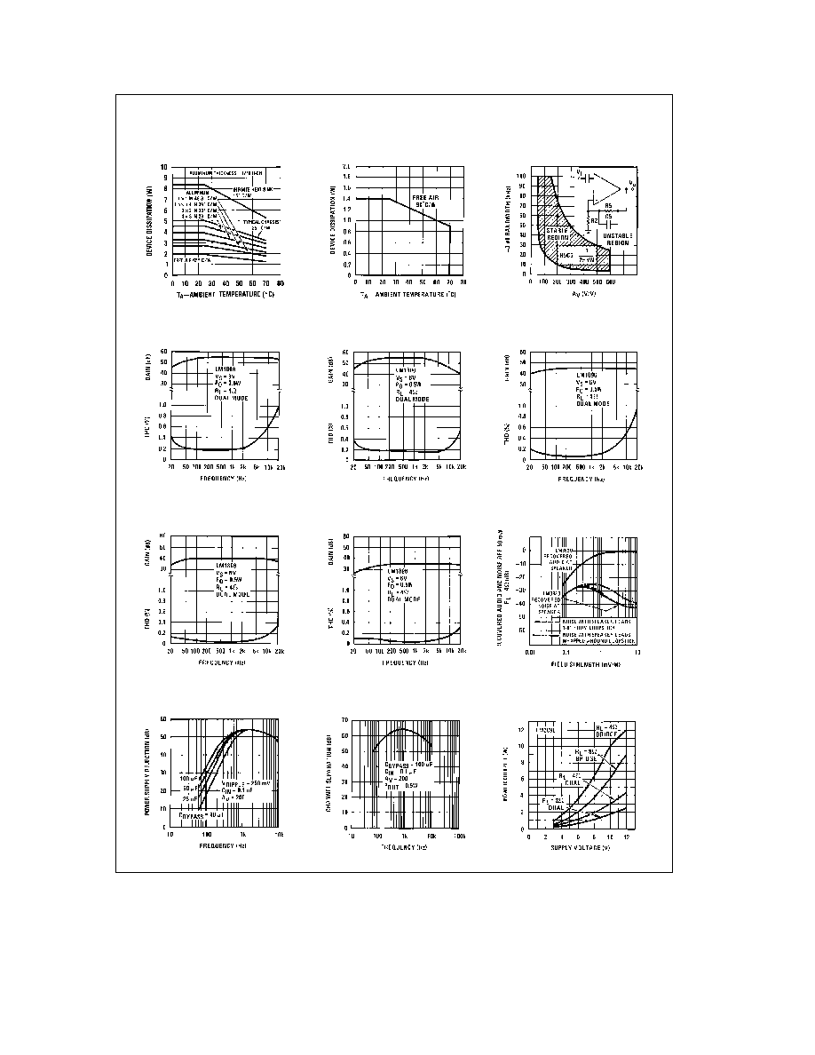
Typical Performance Curves
vs Ambient Temperature
LM2896 Device Dissipation
Temperature
Dissipation vs Ambient
LM1896 Maximum Device
Gain for Stable Operation
b
3 dB Bandwidth vs Voltage
A
V
e
54 dB BW
e
30 kHz
THD and Gain vs Frequency
A
V
e
54 dB BW
e
5 kHz
THD and Gain vs Frequency
A
V
e
46 dB BW
e
50 kHz
THD and Gain vs Frequency
A
V
e
40 dB BW
e
20 kHz
THD and Gain vs Frequency
A
V
e
34 dB BW
e
50 kHz
THD and Gain vs Frequency
Speaker Lead Placement
vs Field Strength for Different
AM Recovered Audio and Noise
vs Frequency
(Referred to the Output)
Power Supply Rejection Ratio
to the Output) vs Frequency
Channel Separation (Referred
Supply Voltage
Power Output vs
TL H 7920 ≠ 2
3
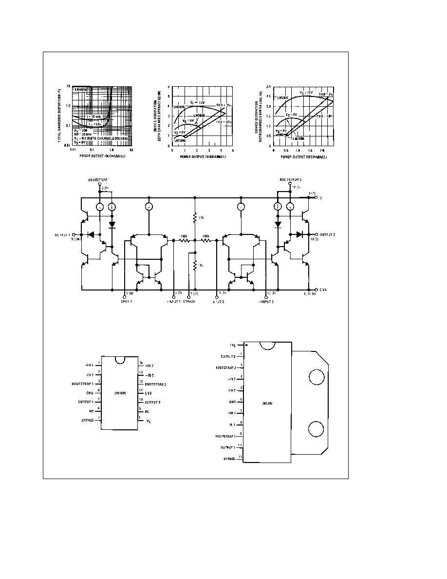
Typical Performance Curves
(Continued)
vs Power Output
Total Harmonic Distortion
Power Output R
L
e
4X
Power Dissipation vs
Power Output R
L
e
8X
Power Dissipation vs
TL H 7920 ≠ 3
Equivalent Schematic
6 9 No connection on LM1896
TL H 7920 ≠ 4
( ) indicates pin number for LM2896
Connection Diagrams
Dual-In-Line Package
TL H 7920 ≠ 5
Top View
Single-In-Line Package
TL H 7920 ≠ 6
Top View
4
Typical Applications
(Continued)
TL H 7920 ≠ 7
6 9 No connection on LM1896
( ) Indicates pin number for LM2896
TL H 7920 ≠ 8
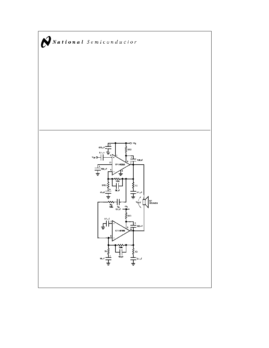
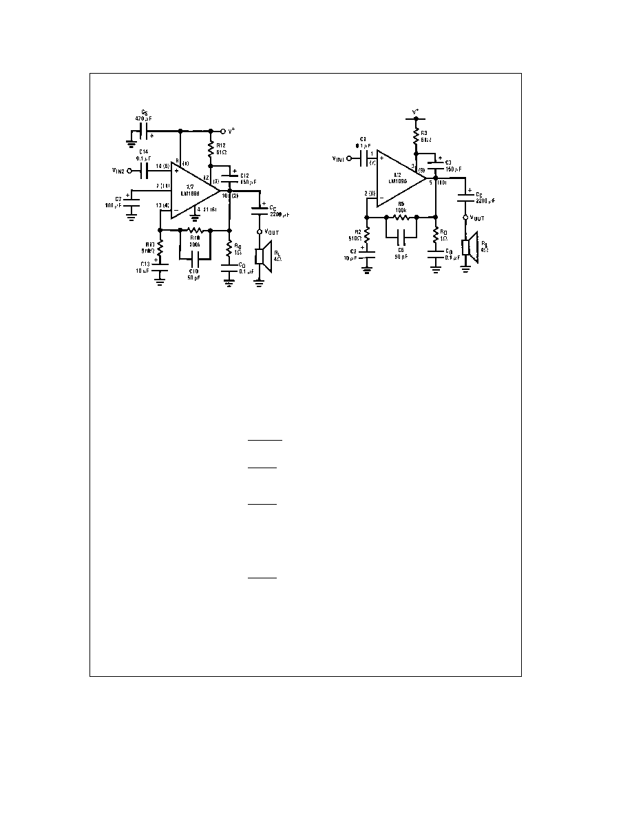
FIGURE 2 Stereo Amplifier with A
V
e
200 BW
e
30 kHz
External Components
(Figure 2)
Components
Comments
1 R2 R5 R10 R13
Sets voltage gain A
V
e
1
a
R5 R2 for one channel and A
V
e
1
a
R10 R13
for the other channel
2 R3 R12
Bootstrap resistor sets drive current for output stage and allows pins 3 and 12 to
go above V
S
3 R
o
Works with C
o
to stabilize output stage
4 C1 C14
Input coupling capacitor Pins 1 and 14 are at a DC potential of V
S
2 Low
frequency pole set by
f
L
e
1
2
q
R
IN
C1
5 C2 C13
Feedback capacitors Ensure unity gain at DC Also a low frequency pole at
f
L
e
1
2
q
R2C2
6 C3 C12
Bootstrap capacitors used to increase drive to output stage A low frequency
pole is set by
f
L
e
1
2
q
R3C3
7 C5 C10
Compensation capacitor These stabilize the amplifiers and adjust their
bandwidth See curve of bandwidth vs allowable gain
8 C7
Improves power supply rejection (See Typical Performance Curves) Increasing
C7 increases turn-on delay
9 C
c
Output coupling capacitor Isolates pins 5 and 10 from the load Low frequency
pole set by
f
L
e
1
2
q
C
c
R
L
10 C
o
Works with R
o
to stabilize output stage
11 C
S
Provides power supply filtering
5