 | –≠–ª–µ–∫—Ç—Ä–æ–Ω–Ω—ã–π –∫–æ–º–ø–æ–Ω–µ–Ω—Ç: LM1921 | –°–∫–∞—á–∞—Ç—å:  PDF PDF  ZIP ZIP |
TL H 5271
LM1921
1
Amp
Industrial
Switch
February 1995
LM1921 1 Amp Industrial Switch
General Description
The LM1921 Relay Driver incorporates an integrated power
PNP transistor as the main driving element The advantages
of this over previous integrated circuits employing NPN
power elements are several Greater output voltages are
available off the same supply for driving grounded loads
typically 4 5 volts for a 500 mA load from a 5 0 volt supply
The output can swing below ground potential up to 57 volts
negative with respect to the positive power supply This can
be used to facilitate rapid decay times in inductive loads
Also the IC is immune to negative supply voltages or tran-
sients The inherent Safe Operating Area of the lateral PNP
allows use of the IC as a bulb driver or for capacitive loads
Familiar integrated circuit features such as short circuit pro-
tection and thermal shutdown are also provided The input
voltage threshold levels are designed to be TTL CMOS
and LSTTL compatible over the entire operating tempera-
ture range If several drivers are used in a system their
inputs and or outputs may be combined and wired together
if their supply voltages are also common
Features
Y
1 Amp output drive
Y
Load connected to ground
Y
Low input-output voltage differential
Y
a
60 volt positive transient protection
Y
b
50 volt negative transient protection
Y
Automotive reverse battery protection
Y
Short circuit proof
Y
Internal thermal overload protection
Y
Unclamped output for fast decay times
Y
TTL LSTTL CMOS compatible input
Y
Plastic TO-220 package
Y
100% electrical burn-in
Applications
Y
Relays
Y
Solenoids
Y
Valves
Y
Motors
Y
Lamps
Y
Heaters
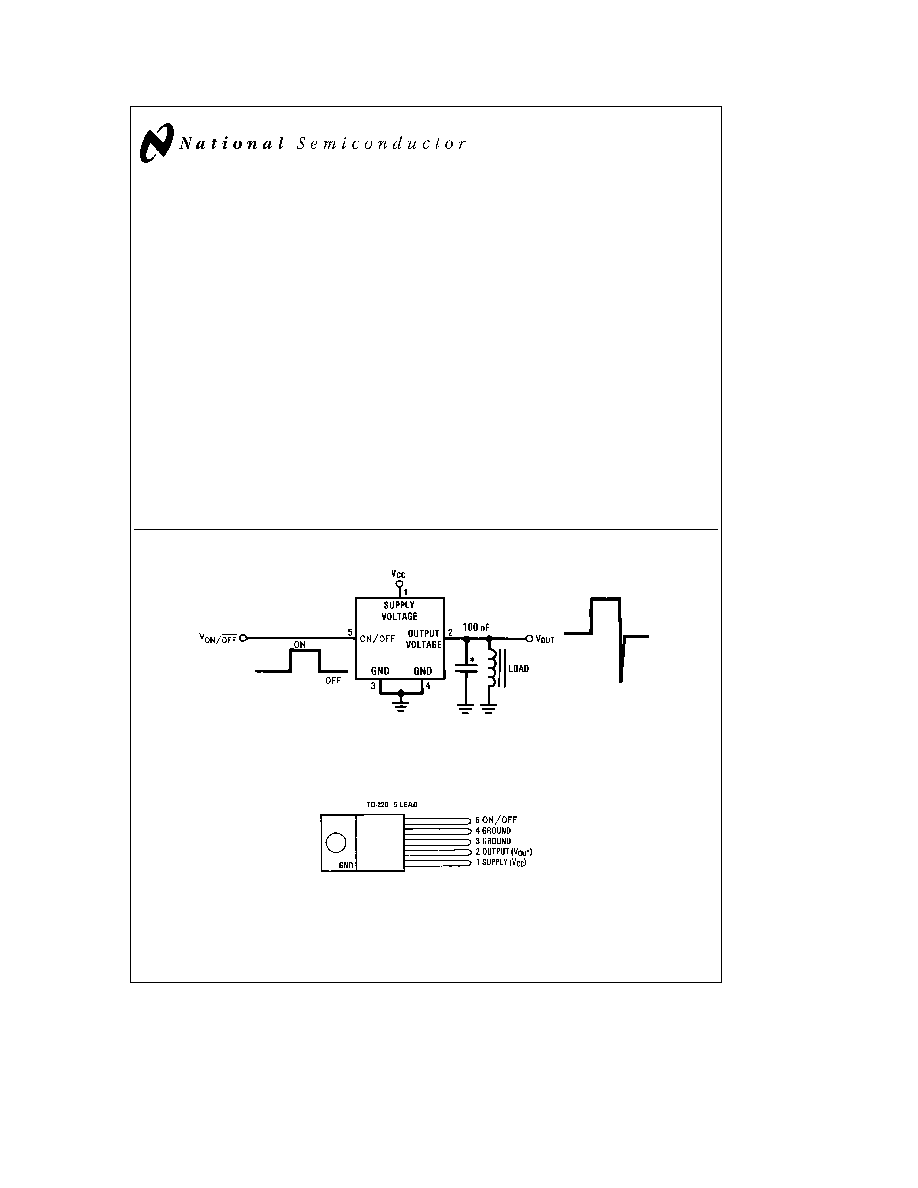
Typical Application Circuit
Required for stability
TL H 5271 ≠ 1
FIGURE 1 Test and Application Circuit
Connection Diagram
TL H 5271 ≠ 2
Front View
Order Number LM1921T
See NS Package Number T05A
C1995 National Semiconductor Corporation
RRD-B30M115 Printed in U S A
Absolute Maximum Ratings
If Military Aerospace specified devices are required
please contact the National Semiconductor Sales
Office Distributors for availability and specifications
Supply Voltage
Operating Range
4 75V to 26V
Overvoltage Protection (100 ms)
b
50V to
a
60V
Internal Power Dissipation
Internally Limited
Operating Temperature Range
b
40 C to
a
125 C
Maximum Junction Temperature
150 C
Storage Temperature Range
b
65 C to
a
150 C
Lead Temp (Soldering 10 seconds)
230 C
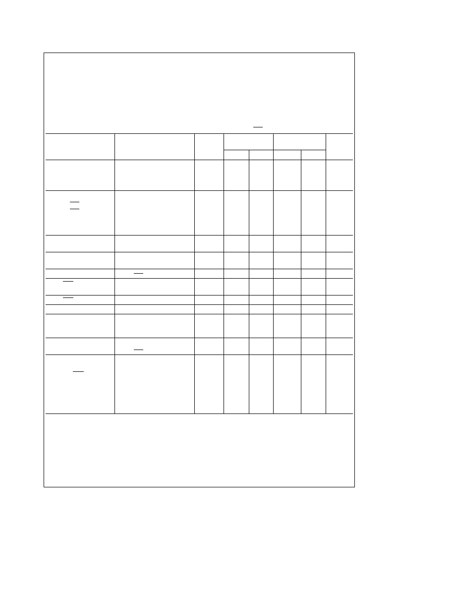
Electrical Characteristics
(V
CC
e
12V I
OUT
e
500 mA T
J
e
25 C V
ON OFF
e
2V unless otherwise specified )
Tested Limits
Design Limits
Parameter
Conditions
Typ
(Note 1)
(Note 2)
Units
Min
Max
Min
Max
Supply Voltage
Operational
4 75
26
6
24
V
Survival
b
15
60
V
DC
Transient
100 ms 1% Duty Cycle
b
50
V
Supply Current
V
ON OFF
e
0
0 6
1 5
mA
V
ON OFF
e
2V
I
OUT
e
0 mA
6
10
mA
I
OUT
e
250 mA
285
350
mA
I
OUT
e
500 mA
575
700
mA
I
OUT
e
1A
1 3
1 5
A
Input to Output
I
OUT
e
500 mA
0 5
0 8
V
Voltage Drop
I
OUT
e
1A
1 0
V
Short Circuit Current
1 4
1 0
2 0
A
6V
s
V
CC
s
24V
75
3 0
A
Output Leakage Current
V
ON OFF
e
0
0 1
50
m
A
ON OFF Voltage
1 3
0 8
2 0
V
Threshhold
6V
s
V
CC
s
24V
0 8
2 0
V
ON OFF Current
15
10
30
m
A
Overvoltage Shutdown
32
26
36
V
Thermal Resistance
junction-case
i
jc
3
C W
case-ambient
i
ca
50
C W
Inductive Clamp
Output Voltage
V
ON OFF
e
0 I
OUT
e
100 mA
b
60
b
120
b
45
V
Fault Conditions
Output Current
ON OFF Floating
Pin 5 Open
0 1
50
m
A
Ground Floating
Pin 3
Pin 4 Open
0 1
50
m
A
Reverse Voltage
V
CC
e b
15V
b
0 01
b
1
mA
Reverse Transient
V
CC
e b
50V
b
100
mA
Overvoltage
V
CC
e a
60V
0 01
1
mA
Supply Current
Pin 1
Pin 2 Short No load
10
40
mA
Note 1
Guaranteed and 100% production tested
Note 2
Guaranteed not necessarily 100% production tested Not used to calculate outgoing AQL Limits are for the temperature range of
b
40 C
s
T
j
s
150 C
2
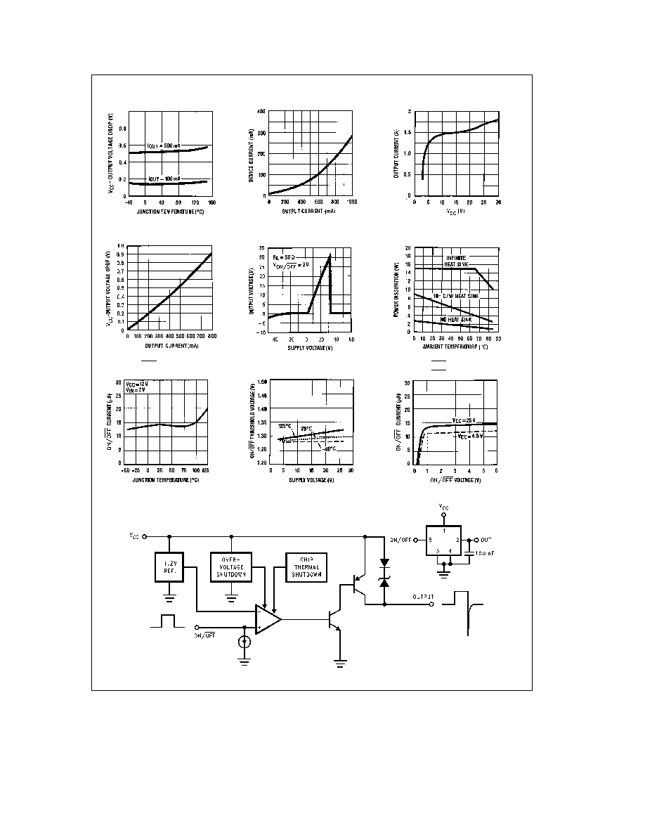
Typical Performance Characteristics
Output Voltage Drop
TL H 5271 ≠ 3
Device Operating Current
TL H 5271 ≠ 4
Peak Output Current (V
OUT
)
TL H 5271 ≠ 5
Output Voltage Drop
TL H 5271 ≠ 6
Output Voltage (V
OUT
)
TL H 5271 ≠ 7
Maximum Power
Dissipation (TO-220)
TL H 5271 ≠ 8
ON OFF Current vs
Junction Temperature
TL H 5271 ≠ 13
Threshold Voltage vs
Supply Voltage
TL H 5271 ≠ 14
ON OFF Current vs
ON OFF Voltage
TL H 5271 ≠ 15
Equivalent Block Diagram
TL H 5271 ≠ 12
FIGURE 1
3
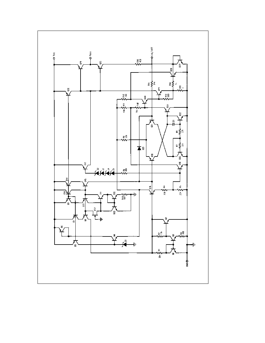
Circuit Schematic
TLH5271
≠
9
4
Application Hints
HIGH CURRENT OUTPUT
The 1 Amp output is fault protected against overvoltage If
the supply voltage rises above approximately 30 volts the
output will automatically shut down This protects the inter-
nal circuitry and enables the IC to survive higher voltage
transients than would otherwise be expected The 1921 will
survive transients and DC voltages up to 60 volts on the
supply The output remains off during this time independent
of the state of the input logic voltage This protects the load
The high current output is also protected against short cir-
cuits to either ground or supply voltage Standard thermal
shutdown circuits are employed to protect the 1921 from
over heating
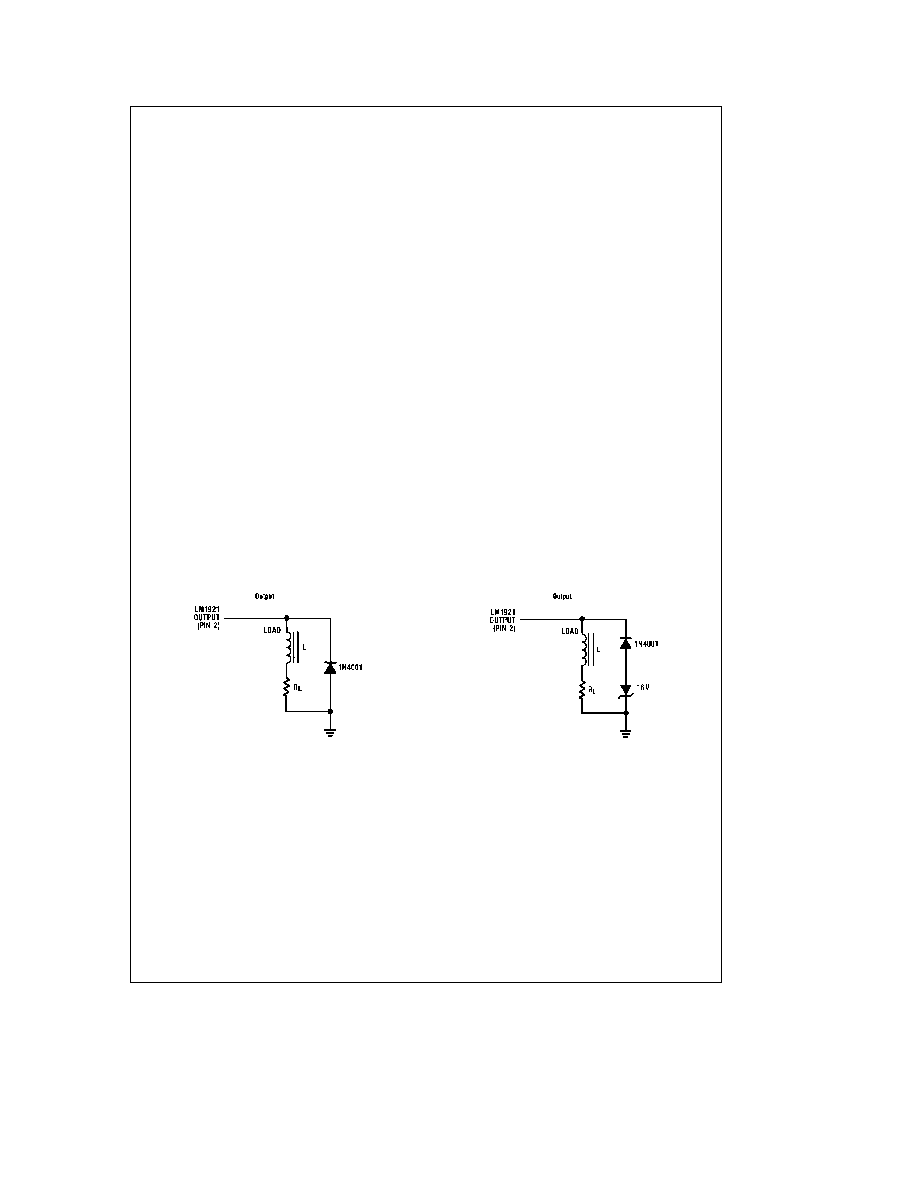
FLYBACK RESPONSE
Since the 1921 is designed to drive inductive as well as any
other type of load inductive kickback can be expected
whenever the output changes state from on to off (see
waveforms on
Figure 1 ) The driver output was left un-
clamped since it is often desirable in many systems to
achieve a very rapid decay in the load current In applica-
tions where this is not true such as in
Figure 2 a simple
external diode clamp will suffice In this application the inte-
grated current in the inductive load is controlled by varying
the duty cycle of the input to the driver IC This technique
achieves response characteristics that are desirable for cer-
tain automotive transmission solenoids for example
For applications requiring a rapid controlled decay in the
solenoid current such as fuel injector drivers an external
zener and diode can be used as in
Figure 3 The voltage
rating of the zener should be such that it breaks down be-
fore the output of the LM1921 The minimum output break-
down voltage of the IC output is rated at
b
57 volts with
respect to the supply voltage Thus on a 12 volt supply the
combined zener and diode breakdown should be less than
45 volts
The LM1921 can be used alone as a simple relay or sole-
noid driver where a rapid decay of the load current is de-
sired but the exact rate of decay is not critical to the sys-
tem If the output is unclamped as in
Figure 1 and the load
is inductive enough the negative flyback transient will cause
the output of the IC to breakdown and behave similarly to a
zener clamp Relying upon the IC breakdown is practical
and will not damage or degrade the IC in any way There are
two considerations that must be accounted for when the
driver is operated in this mode The IC breakdown voltage is
process and lot dependent Clamp voltages ranging from
b
60 to
b
120 volts (with respect to the supply voltage) will
be encountered over time on different devices This is not at
all critical in most applications An important consideration
however is the additional heat dissipated in the IC as a
result This must be added to normal device dissipation
when considering junction temperatures and heat sinking
requirements Worst case for the additional dissipation can
be approximated as
Additional P
D
e
I
2
x L x f (Watts)
where
I
e
peak solenoid current (Amps)
L
e
solenoid inductance (Henries)
f
e
maximum frequency input signal (Hz)
For solenoids where the inductance is less than ten milli-
henries the additional power dissipation can be ignored
Overshoot undershoot and ringing can occur on certain
loads The simple solution is to lower the Q of the load by
the addition of a resistor in parallel or series with the load A
value that draws one tenth of the current or DC voltage of
the load is usually sufficient
TL H 5271 ≠ 10
FIGURE 2 Diode Clamp
TL H 5271 ≠ 11
FIGURE 3
Zener clamp for rapid controlled current decay
5