TL H 9133
LM1951
Solid
State
1
Amp
Switch
August 1992
LM1951 Solid State 1 Amp Switch
General Description
The LM1951 is a high current high voltage high side (PNP)
switch with a built-in error detection circuit
The LM1951 is guaranteed to deliver 1 Amp output current
and is capable of withstanding up to
g
85V transients The
built-in error detection provides an error flag output under
the following fault conditions output short to ground or sup-
ply open load current limit overvoltage or thermal shut-
down The LM1951 will drive all types of resistive or induc-
tive loads The output has a built-in negative voltage clamp
(
b
30V) to provide a quick energy discharge path for
inductive loads The LM1951 features TTL and CMOS com-
patible logic input with hysteresis Switching times both turn
on and turn off are 2 ms (C
load
k
0 005 mF) In addition its
quiescent current in the OFF state is typically less than
0 1 mA at room temperature and less than 10 mA over the
entire operating temperature and voltage range
The LM1951 features make it well suited for industrial and
automotive applications
Features
Y
0 1 mA typical quiescent current (OFF state)
Y
1 Amp output current guaranteed
Y
g
85V transient protection
Y
Reverse voltage protection
Y
Negative output voltage clamp
Y
Error flag output
Y
Internal overvoltage shutdown
Y
Internal thermal shutdown
Y
Short circuit proof
Y
High speed switching (up to 50 kHz)
Y
Inductive or resistive loads
Y
Low ON resistance (1X maximum)
Y
TTL CMOS compatible input with hysteresis
Y
Plastic TO-220 5-lead package
Y
ESD protected
Y
4 5V to 26V operation
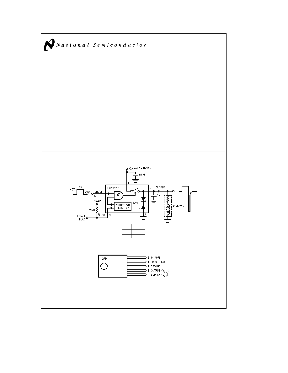
Typical Application Circuit and Connection Diagram
TL H 9133 ≠ 1
V
IN
Output
0
OFF
1
ON
TO-220 5-Lead
TL H 9133 ≠ 2
Front View
Order Number LM1951T
See NS Package Number T05A
C1995 National Semiconductor Corporation
RRD-B30M115 Printed in U S A
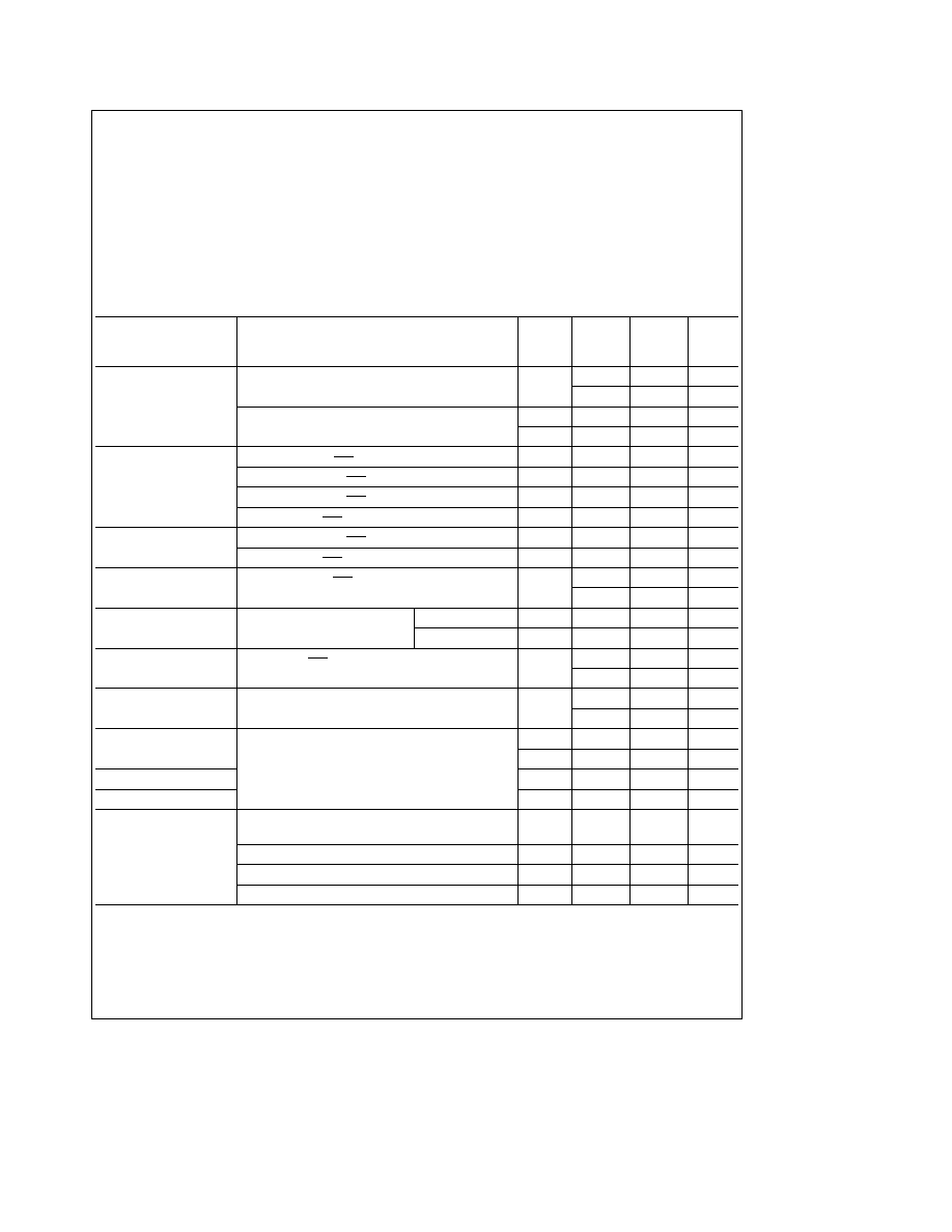
Absolute Maximum Ratings
If Military Aerospace specified devices are required
please contact the National Semiconductor Sales
Office Distributors for availability and specifications
Supply Voltage
Operational Voltage
26 V
DC
Sustained Voltage
b
40 V
DC
t
V
CC
s
85 V
DC
Transient Voltage Protection
g
85V
(
u
e
100 ms 1% Duty Cycle R
S
t
10X)
Pins 4 5
26 V
DC
Power Dissipation (Note 1)
Internally Limited
Load Inductance
1H
Operating Temperature Range (T
A
)
b
40 C to
a
125 C
Maximum Junction Temperature
150 C
Storage Temperature Range
b
65 C to
a
150 C
Lead Temperature (Soldering 10 sec )
260 C
ESD Tolerance (Note 4)
2000V
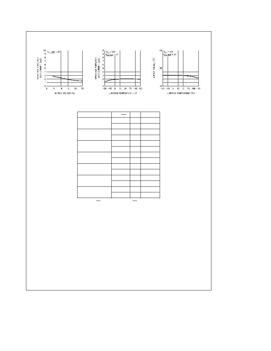
Electrical Characteristics
V
CC
e
12V I
out
e
500 mA C
out
e
0 001 mF T
A
e
25 C unless otherwise specified
Tested
Design
Parameter
Conditions
Typical
Limit
Limit
Units
(Note 2)
(Note 3)
Supply Voltage V
CC
4 5
V
min
Operational
26
V
max
Transient
u
e
100 ms 1% Duty Cycle R
CC
t
10X
b
85
V
85
V
Supply Current
I
out
e
0 mA V
ON OFF
e
0 8V
0 1
10
100
m
A
max
I
out
e
250 mA V
ON OFF
e
2 0V
260
270
mA
max
I
out
e
600 mA V
ON OFF
e
2 0V
630
650
mA
max
I
out
e
1A V
ON OFF
e
2 0V
1 06
1 2
A
max
Voltage Drop
I
out
e
600 mA V
ON OFF
e
2 0V
400
600
mV
max
(V
CC
b
V
OUT
)
I
out
e
1A V
ON OFF
e
2 0V
0 7
1 0
V
max
Short Circuit Current
V
OUT
e
0V V
ON OFF
e
2V
1 3
1 0
A
min
2 5
A
max
Input Threshold Pin 5
4 5V
s
V
CC
s
26V
Turn ON
1 4
2 0
2 0
V
max
Turn OFF
1 2
0 8
0 8
V
min
Input Current Pin 5
0 8V
s
V
ON OFF
s
5 5V
25
50
m
A
max
10
m
A
min
Output Clamp
I
out
s
600 mA
b
30
b
40
V
min
b
24
V
max
Delay
t
d
ON
R
load
e
20X C
load
e
0 001 mF
1
3
m
s
max
Time
t
d
OFF
1
3
m
s
max
Rise Time
1
3
m
s
max
Fall Time
1
3
m
s
max
Error Flag Characteristics
Output Voltage
Error Condition Pin 4 Low Sinking 10 mA
0 3
0 8
V
max
Sink Current
Error Condition Pin 4
e
0 3V
10
3
mA
min
Output Leakage Current
No Error Pin 4
e
26V
0 01
1
m
A
max
Response Time
V
LOGIC
e
5V R
LOGIC
e
2 kX C
LOGIC
e
0 mF
1
m
s
Note 1
Thermal resistance junction-to-case is 3 C W Thermal resistance case-to-ambient is 50 C W
Note 2
Tested Limits are guaranteed and 100% production tested
Note 3
Design Limits are guaranteed (but not 100% production tested) over the operating temperature and supply voltage range These limits are not used to
calculate outgoing quality levels
Note 4
Human body model 100 pF discharged through a 1 5 kX resistor
2
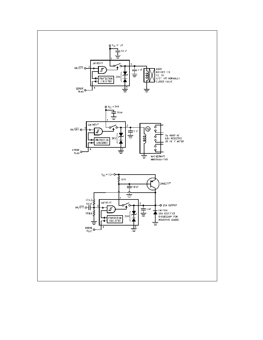
Typical Applications
TL H 9133 ≠ 4
FIGURE 1 Solenoid Actuated Valve
TL H 9133 ≠ 5
FIGURE 2 60A 3-Phase Mercury Displacement Relay
TL H 9133 ≠ 6
Available from Germanium Power Devices Andover MA Tel (617) 475-5982
FIGURE 3 25A Switch with Short Circuit Foldback
5