 | –≠–ª–µ–∫—Ç—Ä–æ–Ω–Ω—ã–π –∫–æ–º–ø–æ–Ω–µ–Ω—Ç: LM1973MX | –°–∫–∞—á–∞—Ç—å:  PDF PDF  ZIP ZIP |
LM1973
µPot
TM
3-Channel 76dB Audio Attenuator with Mute
General Description
The LM1973 is a digitally controlled 3-channel 76dB audio
attenuator fabricated on a CMOS process. Each channel
has attenuation steps of 0.5dB from 0dB≠15.5dB, 1.0dB
steps from 16dB≠47dB, and 2.0dB steps from 48dB≠ 76dB,
with a mute function attenuating 104dB. Its logarithmic at-
tenuation curve can be customized through software to fit
the desired application.
The performance of a µPot
TM
is demonstrated through its ex-
cellent Signal-to-Noise Ratio, extremely low (THD+N), and
high channel separation. Each µPot contains a mute function
that disconnects the input signal from the output, providing a
minimum attenuation of 96dB. Transitions between any at-
tenuation settings are pop free.
The LM1973's 3-wire serial digital interface is TTL and
CMOS compatible; receiving data that selects a channel and
the desired attenuation level. The Data-Out pin of the
LM1973 allows multiple µPots to be daisy-chained together,
reducing the number of enable and data lines to be routed
for a given application.
Key Specifications
n
Total Harmonic Distortion + Noise:
0.003% (max)
n
Frequency response:
100 kHz (-3dB) (min)
n
Attenuation range (excluding mute):
76dB (typ)
n
Differential attenuation:
±
0.25dB (max)
n
Signal-to-noise ratio (ref. 4 Vrms):
110dB (min)
n
Channel separation:
110dB (typ)
Features
n
3-wire serial interface
n
Daisy-chain capability
n
104dB mute attenuation
n
Pop and click free attenuation changes
Applications
n
Automated studio mixing consoles
n
Music reproduction systems
n
Sound reinforcement systems
n
Electronic music (MIDI)
n
Personal computer audio control
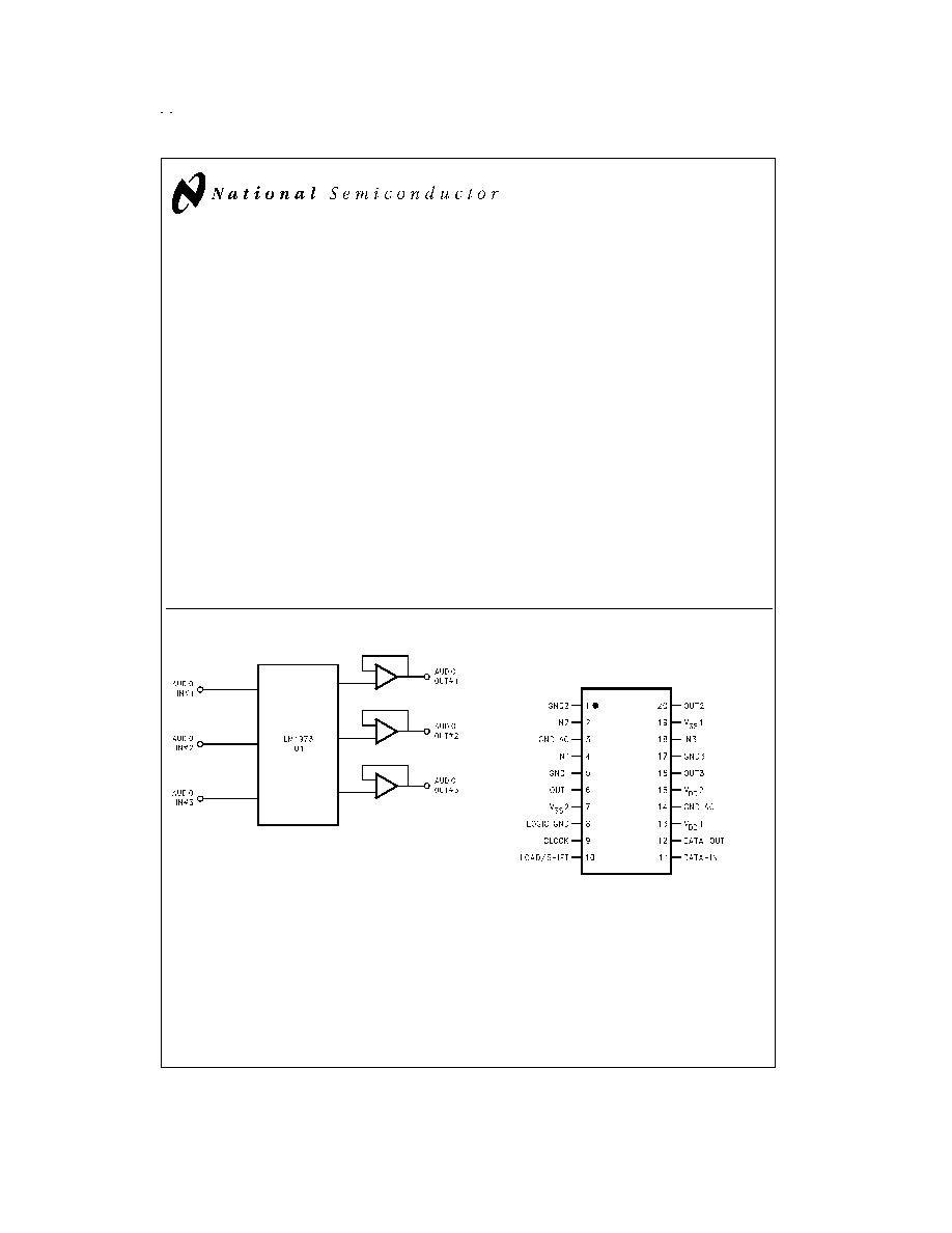
Typical Application
Connection Diagram
µPot
TM
and Overture
TM
are trademarks of National Semiconductor Corporation.
DS011958-1
FIGURE 1. Typical Audio Attenuator
Application Circuit
Dual-In-Line Plastic or
Surface Mount Package
DS011958-2
Top View
Order Number LM1973M or LM1973N
See NS Package Number M20B or N20A
December 1994
LM1973
µPot
3-Channel
76dB
Audio
Attenuator
with
Mute
© 1999 National Semiconductor Corporation
DS011958
www.national.com
Absolute Maximum Ratings
(Notes 1, 2)
If Military/Aerospace specified devices are required,
please contact the National Semiconductor Sales Office/
Distributors for availability and specifications.
Supply Voltage (V
DD
≠V
SS
)
15V
Voltage at Any Pin
V
SS
- 0.2V to V
DD
+ 0.2V
Power Dissipation (Note 3)
150 mW
ESD Susceptability (Note 4)
1800V
Junction Temperature
150∞C
Soldering Information
N Package (10 sec.)
+260∞C
Storage Temperature
-65∞C to +150∞C
Operating Ratings
(Notes 1, 2)
T
MIN
T
A
T
MAX
Temperature Range
T
MIN
T
A
T
MAX
0∞C
T
A
+70∞C
Supply Voltage (V
DD
- V
SS
)
4.5V to 12V
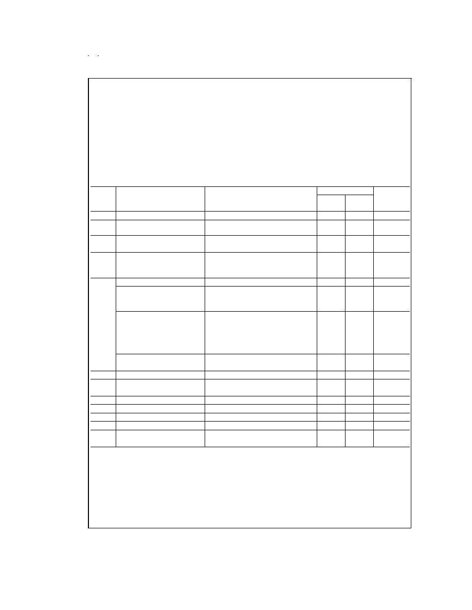
Electrical Characteristics
(Notes 1, 2)
The following specifications apply for all channels with V
DD
= +6V, V
SS
= -6V, V
IN
= 5.5 Vpk, and f = 1 kHz, unless otherwise
specified. Limits apply for T
A
= 25∞C. Digital inputs are TTL and CMOS compatible.
Symbol
Parameter
Conditions
LM1973
Units
(Limits)
Typical
Limit
(Note 5)
(Note 6)
I
S
Supply Current
Inputs are AC Grounded
3
5
mA (max)
THD+N
Total Harmonic Distortion
plus Noise
V
IN
= 0.5 Vpk
@
0dB Attenuation
0.0008
0.003
% (max)
XTalk
Crosstalk (Channel Separation)
0dB Attenuation for V
IN
110
dB
(Note 7)
V
CH
measured
@
-76dB
SNR
Signal-to-Noise Ratio
Inputs are AC Grounded
@
-12dB Attenuation
120
110
dB (min)
A-Weighted
A
M
Mute Attenuation
104
96
dB (min)
Attenuation Step Size Error
0dB to -16dB
±
0.05
dB (max)
-17dB to -48dB
±
0.1
dB (max)
-49dB to -76dB
±
0.25
dB (max)
Absolute Attenuation Error
Attenuation
@
0dB
0.01
0.5
dB (min)
Attenuation
@
-20dB
19.8
19.0
dB (min)
Attenuation
@
-40dB
39.5
38.5
dB (min)
Attenuation
@
-60dB
59.3
58.0
dB (min)
Attenuation
@
-76dB
74.5
73.0
dB (min)
Channel-to-Channel Attenuation
Attenuation
@
0dB, -20dB, -40dB, -60dB
±
0.5
dB (max)
Tracking Error
Attenuation
@
-76dB
±
0.75
dB (max)
I
LEAK
Analog Input Leakage Current
Inputs are AC Grounded
10.0
100
nA (max)
R
IN
AC Input Impedance
Pins 2, 4, 18, V
IN
= 1.0 Vpk, f = 1 kHz
40
20
k
(min)
60
k
(max)
I
IN
Input Current
@
Pins 9, 10, 11
@
0V
<
V
IN
<
5V
1.0
±
100
nA (max)
f
CLK
Clock Frequency
3
2
MHz (max)
V
IH
High-Level Input Voltage
@
Pins 9, 10, 11
2.0
V (min)
V
IL
Low-Level Input Voltage
@
Pins 9, 10, 11
0.8
V (max)
Data-Out Levels (Pin 12)
V
DD
=6V, V
SS
=0V
0.1
V (max)
5.9
V (min)
Note 1:
Absolute Maximum Ratings indicate limits beyond which damage to the device may occur. Operating Ratings indicate conditions for which the device is func-
tional, but do not guarantee specific performance limits.
Electrical Characteristics state DC and AC electrical specifications under particular test conditions which guar-
antee specific performance limits. This assumes that the device is within the Operating Ratings. Specifications are not guaranteed for parameters where no limit is
given, however, the typical value is a good indication of device performance.
Note 2: All voltages are measured with respect to GND (pins 1, 3, 5, 14, 17), unless otherwise specified.
Note 3: The maximum power dissipation must be derated at elevated temperatures and is dictated by T
JMAX
,
JA
, and the ambient temperature T
A
. The maximum
allowable power dissipation is PD = (T
JMAX
- T
A
)/
JA
or the number given in the Absolute Maximum Ratings, whichever is lower. For the LM1973N, T
JMAX
= +150∞C,
and the typical junction-to-ambient thermal resistance, when board mounted, is 65∞C/W.
Note 4: Human body model, 100 pF discharged through a 1.5 k
resistor.
Note 5: Typicals are measured at 25∞C and represent the parametric norm.
Note 6: Limits are guaranteed to National's AOQL (Average Output Quality Level).
Note 7: At the present time the Crosstalk measurement is specified as a typical only, which is due to a hardware limitation of the automated test equipment.
www.national.com
2
Electrical Characteristics
(Notes 1, 2) (Continued)
Pin Description
Signal Ground (1, 5, 17): Each input has its own indepen-
dent ground, GND1, GND2, and GND3.
Signal Input (2, 4, 18): There are 3 independent signal in-
puts, IN1, IN2, and IN3.
Signal Output (6, 16, 20): There are 3 independent signal
outputs, OUT1, OUT2, and OUT3.
Voltage Supply (13, 15): Positive voltage supply pins, V
DD1
and V
DD2
.
Voltage Supply (7, 19): Negative voltage supply pins, V
SS1
and V
SS2
. To be tied to ground in a single supply configura-
tion.
AC Ground (3, 14): These two pins are not physically con-
nected to the die in any way (i.e., No bondwires). These pins
must be AC grounded to prevent signal coupling between
any of the pins nearby. Pin 14 should be connected to pins
13 and 15 for ease of wiring and the best isolation.
Logic Ground (8): Digital signal ground for the interface
lines; CLOCK, LOAD/SHIFT, DATA-IN and DATA-OUT.
Clock (9): The clock input accepts a TTL or CMOS level sig-
nal. The clock input is used to load data into the internal shift
register on the rising edge of the input clock waveform.
Load/Shift (10): The load/shift input accepts a TTL or
CMOS level signal. This is the enable pin of the device, al-
lowing data to be clocked in while this input is low (0V).
Data-In (11): The data-in input accepts a TTL or CMOS level
signal. This pin is used to accept serial data from a micro-
controller that will be latched and decoded to change a chan-
nel's attenuation level.
Data-Out (12): This pin is used in daisy-chain mode where
more than one µPot is controlled via the same data line. As
the data is clocked into the chain from the µC, the preceding
data in the shift register is shifted out the DATA-OUT pin to
the next µPot in the chain or to ground if it is the last µPot in
the chain. The LOAD/SHIFT line goes high once all of the
new data has been shifted into each of its respective regis-
ters.
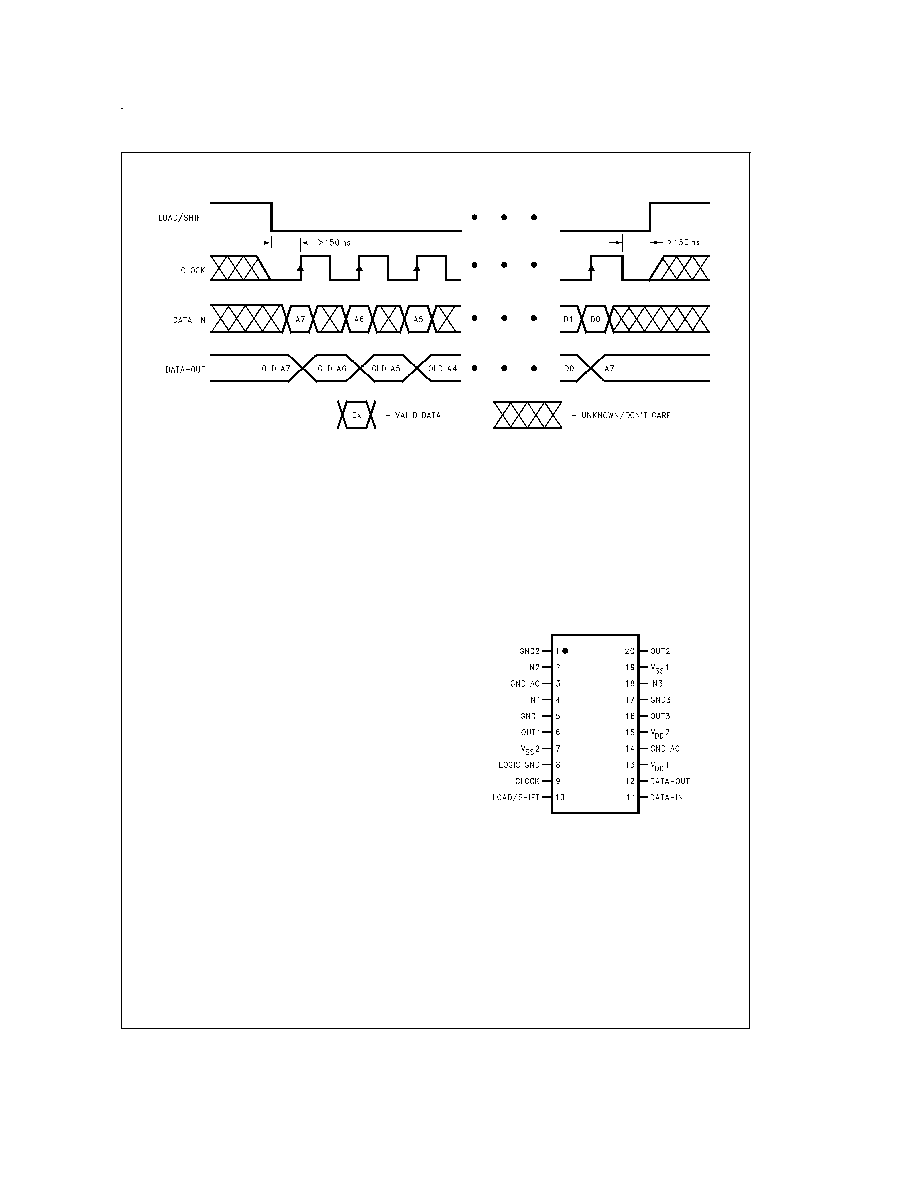
Connection Diagram
DS011958-3
FIGURE 2. Timing Diagram
DS011958-2
www.national.com
3
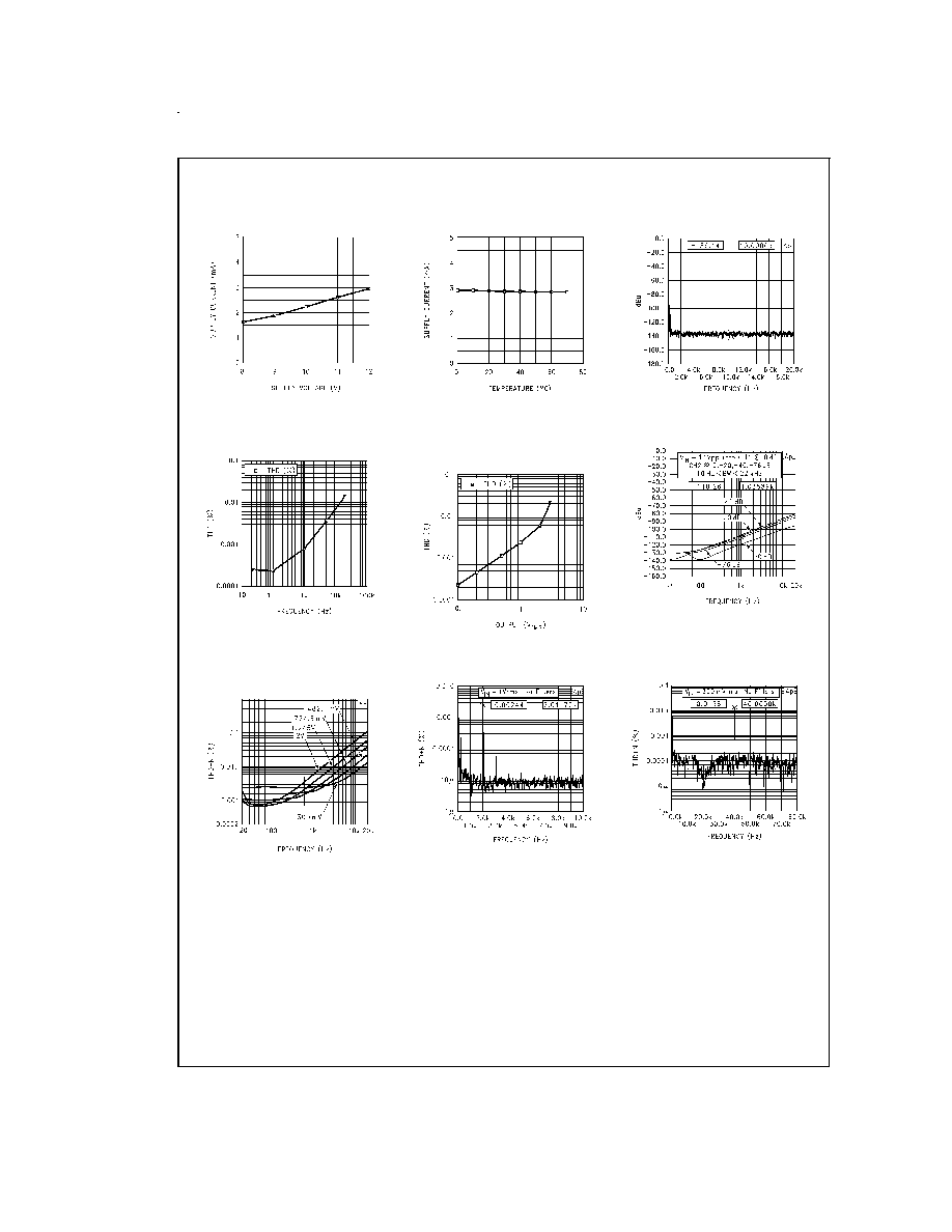
Typical Performance Characteristics
Supply Current vs
Supply Voltage
DS011958-16
Supply Current vs
Temperature
DS011958-17
Noise Floor Spectrum by FFT
Amplitude vs Frequency
DS011958-18
THD vs Freq by FFT
V
DD
- V
SS
= 12V
DS011958-19
THD vs V
OUT
at
1 kHz by FFT
V
DD
- V
SS
= 12V
DS011958-20
Crosstalk Test
DS011958-21
THD + N vs
Frequency and Amplitude
DS011958-22
FFT of 1 kHz THD
DS011958-23
FFT of 20 kHz THD
DS011958-24
www.national.com
4
Typical Performance Characteristics
(Continued)
Application Information
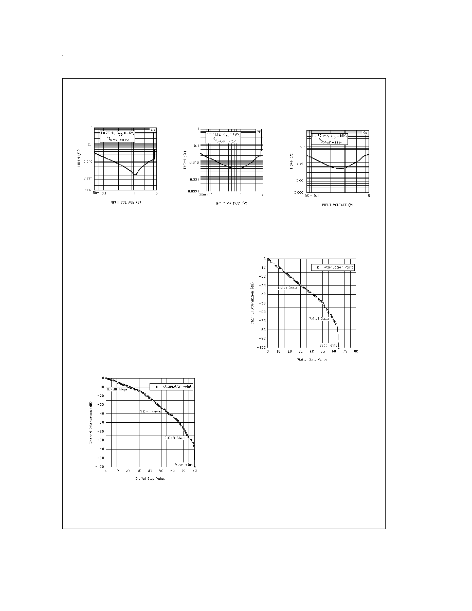
ATTENUATION STEP SCHEME
The fundamental attenuation step scheme for the LM1973
µPot is shown in
Figure 3. This attenuation step scheme,
however, can be changed through programming techniques
to fit different application requirements. One such example
would be a constant logarithmic attenuation scheme of 2dB
steps for a panning function as shown in
Figure 5. The only
restriction to the customization of attenuation schemes are
the given attenuation levels and their corresponding data
bits shown in
Table 1. The device will change attenuation
levels only when a channel address is recognized. When
recognized, the attenuation level will be changed corre-
sponding to the data bits shown in
Table 1. As shown in Fig-
ure 6, an LM1973 can be configured with a mono audio sig-
nal level control and with a panning control which separates
the mono signal into left and right channels. This circuit may
utilize the fundamental attenuation scheme of the LM1973
for the level control, but also possess a constant 2dB pan-
ning control for the left and right channels as stated earlier.
THD + N vs Amplitude
f = 20 Hz, V
DD
=
±
6V
V
IN
into CH1
@
0 dB
DS011958-25
THD + N vs Amplitude
f = 1 kHz, V
DD
=
±
6V
V
IN
into CH1
@
0 dB
DS011958-26
THD + N vs Amplitude
f = 20 kHz, V
DD
=
±
6V
V
IN
into CH1
@
0 dB
DS011958-27
LM1973 Channel Attenuation
vs Digital Step Value
DS011958-7
FIGURE 3. LM1973 Attenuation Step Scheme
LM1973 Channel Attenuation
vs Digital Step Value
(Programmed 1.0dB Steps)
DS011958-14
FIGURE 4. LM1973 1.0dB and 2.0dB
Attenuation Step Scheme
www.national.com
5