 | –≠–ª–µ–∫—Ç—Ä–æ–Ω–Ω—ã–π –∫–æ–º–ø–æ–Ω–µ–Ω—Ç: LM2005T-M | –°–∫–∞—á–∞—Ç—å:  PDF PDF  ZIP ZIP |
TL H 5129
LM2005
20
Watt
Automotive
Power
Amplifier
April 1989
LM2005 20 Watt Automotive Power Amplifier
General Description
The LM2005 is a dual high power amplifier designed to
deliver optimum performance and reliability for automotive
applications High current capability (3 5A) enables the de-
vice to deliver 10W channel into 2X (LM2005T-S) or 20W
bridged monaural (LM2005T-M) into 4X with low distortion
Features
Y
Wide supply range (8V ≠ 18V)
Y
Externally programmable gain
Y
With or without bootstrap
Y
Low distortion
Y
Low noise
Y
High peak current capability
Y
P
O
e
20W bridge
Y
High voltage protection
Y
AC and DC output short circuit protection to ground or
across load
Y
Thermal protection
Y
Inductive load protection
Y
Accidental open ground protection
Y
Immunity to 40V power supply transients
Y
3 C W device dissipation
Y
Pin for pin compatible with TDA2005
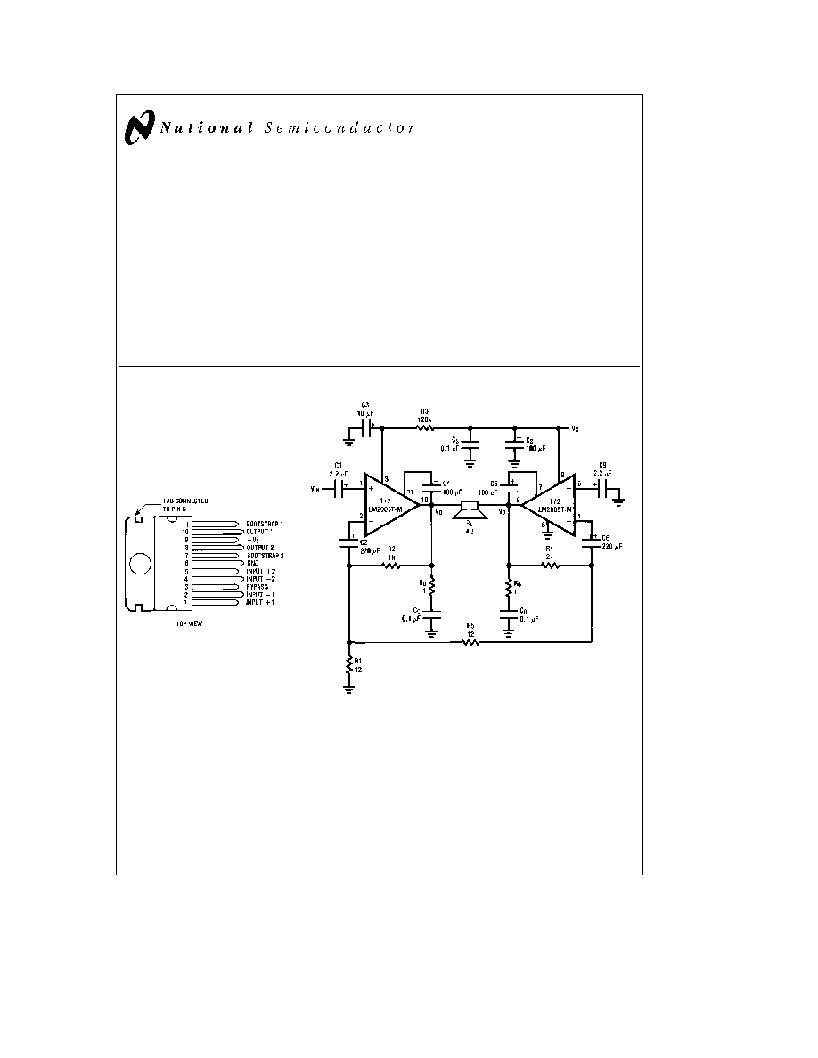
Connection Diagram
Plastic Package
TL H 5129 ≠ 1
Order Number LM2005T-S
or LM2005T-M
See NS Package Number TA11A
Typical Application
TL H 5129 ≠ 2
FIGURE 1 20W Bridge Amplifier Application and Test Circuit
C1995 National Semiconductor Corporation
RRD-B30M115 Printed in U S A
LM2005T-M and LM2005T-S
Absolute Maximum Ratings
If Military Aerospace specified devices are required
please contact the National Semiconductor Sales
Office Distributors for availability and specifications
Operating Supply Voltage
18V
DC Supply Voltage (Note 1)
28V
Peak Supply Voltage (50 ms)
40V
Output Current
Repetitive (Note 2)
3 5A
Non-Repetitive
4 5A
Power Dissipation
30W
Operating Temperature
b
40 C to
a
85 C
Storage Temperature
b
60 C to
a
150 C
Lead Temp (Soldering 10 seconds)
260 C
LM2005T-M
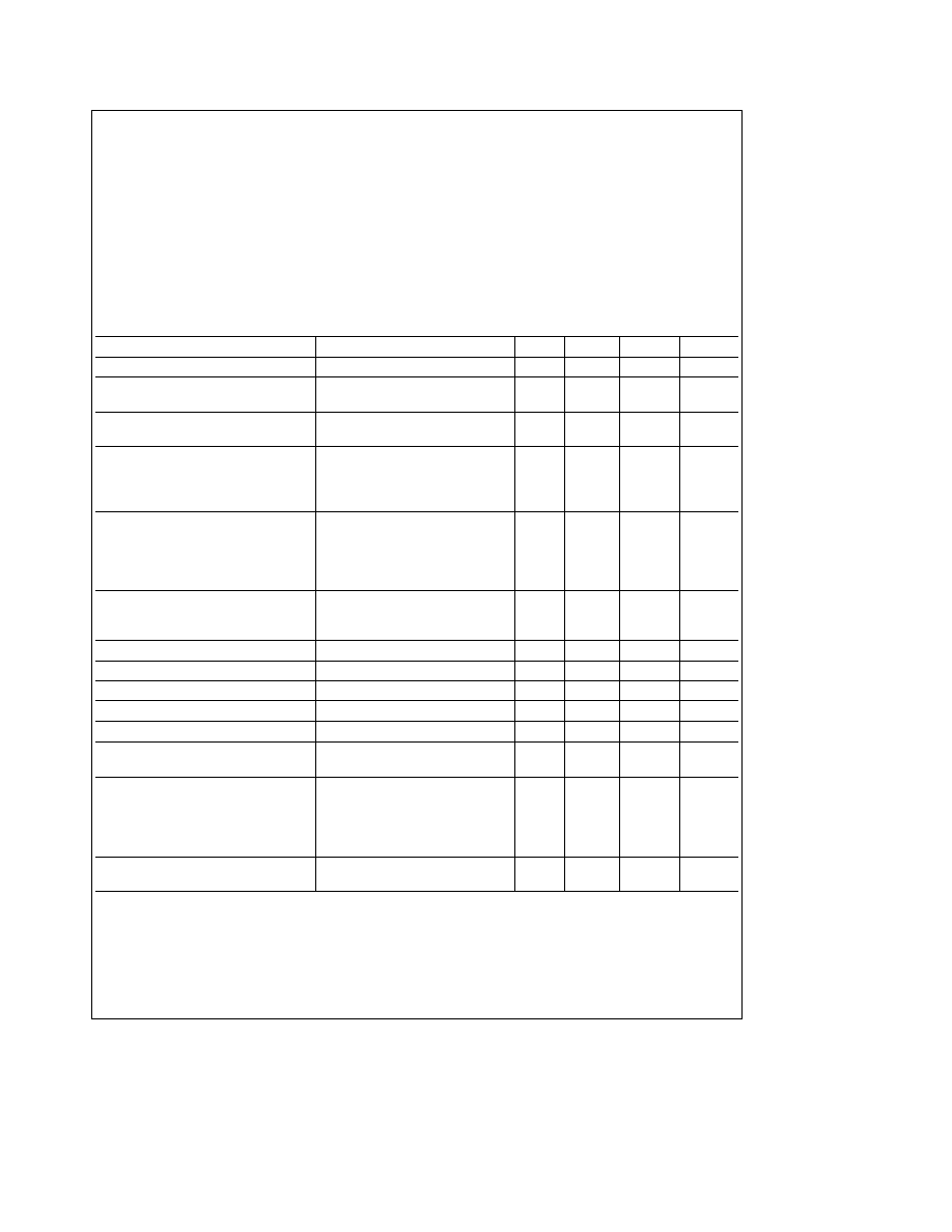
Electrical Characteristics
Refer to the bridge application circuit
Figure 1 T
amb
e
25 C A
V
e
50 dB
R
th (heatsink)
e
4 C W unless otherwise specified
Parameter
Test Conditions
Min
Typ
Max
Units
Supply Voltage
8
18
V
Output Offset Voltage (Note 3)
V
S
e
14 4V
g
20
g
150
mV
(between Pin 8 and 10)
V
S
e
13 2V
g
150
mV
Total Quiescent Drain Current
V
S
e
14 4V
R
L
e
4X
75
150
mA
Includes Current in Feedback Resistors
V
S
e
13 2V
R
L
e
3 2X
70
160
mA
Output Power
d
e
10%
f
e
1 kHz
V
S
e
14 4V
R
L
e
4X
18
20
W
R
L
e
3 2X
20
22
W
V
S
e
13 2V
R
L
e
3 2X
17
19
W
THD
f
e
1 kHz
V
S
e
14 4V
R
L
e
4X
P
O
e
50 mW to 15W
1
%
V
S
e
13 2V
R
L
e
3 2X
P
O
e
50 mW to 13W
1
%
Input Sensitivity
f
e
1 kHz
P
O
e
2W
R
L
e
4X
9
mV
P
O
e
2W
R
L
e
3 2X
8
mV
Input Resistance
f
e
1 kHz
70
kX
Low Frequency Roll Off (
b
3 dB)
R
L
e
3 2X
40
Hz
High Frequency Roll Off (
b
3 dB)
R
L
e
3 2X
20
kHz
Closed Loop Voltage Gain
f
e
1 kHz
45
50
dB
Total Input Noise Voltage
R
g
e
10 kX (Note 4)
3
10
m
V
Supply Voltage Rejection
R
g
e
10 kX
f
ripple
e
100 Hz
45
55
dB
C
4
e
10 mF
V
ripple
e
0 5V
Efficiency
V
S
e
14 4V
f
e
1 kHz
P
O
e
20W
R
L
e
4X
60
%
P
O
e
22W
R
L
e
3 2X
60
%
V
S
e
13 2V
f
e
1 kHz
P
O
e
19W
R
L
e
3 2X
58
%
Output Voltage with One Side
V
S
e
14 4V
R
L
e
4X
2
V
of the Speaker Shorted to Ground
V
S
e
13 2V
R
L
e
3 2V
Note 1
Internal voltage limit Shuts down above 20V
Note 2
Internal current limit
Note 3
For LM2005T-M only
Note 4
Bandwidth filter 22 Hz to 22 kHz
2
LM2005T-S
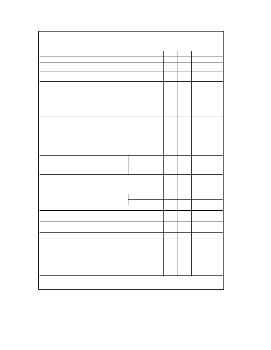
Electrical Characteristics
Refer to the stereo application circuit
Figure 2 T
amb
e
25 C G
v
e
50 dB
R
th (heatsink)
e
4 C W unless otherwise specified
Parameter
Test Conditions
Min
Typ
Max
Units
Supply Voltage
8
18
V
Quiescent Output Voltage
V
S
e
14 4V
6 6
7 2
7 8
V
V
S
e
13 2V
6
6 6
7 2
V
Total Quiescent Drain Current
V
S
e
14 4V
65
120
mA
Includes Current in Feedback Resistors
V
S
e
13 2V
62
120
mA
Output Power
f
e
1 kHz
d
e
10%
(Each Channel)
V
S
e
14 4V
R
L
e
4X
6
6 5
W
R
L
e
3 2X
7
8
W
R
L
e
2X
9
10
W
R
L
e
1 6X
10
11
W
V
S
e
13 2V
R
L
e
3 2X
6
6 5
W
R
L
e
1 6X
9
10
W
V
S
e
16V
R
L
e
2X
12
W
THD
f
e
1 kHz
(Each Channel)
V
S
e
14 4V
R
L
e
4X
P
O
e
50 mW to 4W
0 2
1
%
V
S
e
14 4V
R
L
e
2X
P
O
e
50 mW to 6W
0 3
1
%
V
S
e
13 2V
R
L
e
3 2X
P
O
e
50 mW to 3W
0 2
1
%
V
S
e
13 2V
R
L
e
1 6X
P
O
e
40 mW to 6W
0 3
1
%
Cross Talk
V
S
e
14 4V
f
e
1 kHz
40
60
dB
(Note 5)
R
L
e
4X
V
O
e
4 V
rms
f
e
10 kHz
40
dB
R
g
e
5 kX
Input Saturation Voltage
300
mV
Input Sensitivity
f
e
1 kHz
P
O
e
1W
R
L
e
4X
6
mV
R
L
e
3 2X
5 5
Input Resistance
f
e
1 kHz
Non-Inverting Input
70
200
kX
Inverting Input
10
kX
Low Frequency Roll Off (
b
3 dB)
R
L
e
2X
50
Hz
High Frequency Roll Off (
b
3 dB)
R
L
e
2X
15
kHz
Voltage Gain (Open Loop)
f
e
1 kHz
90
dB
Voltage Gain (Closed Loop)
f
e
1 kHz
48
50
51
dB
Closed Loop Gain Matching
0 5
dB
Total Input Noise Voltage
R
g
e
10 kX (Note 6)
1 5
5
m
V
Supply Voltage Rejection
R
g
e
10 kX
f
ripple
e
100 Hz
35
45
dB
C
3
e
10 mF
V
ripple
e
0 5V
Efficiency
V
S
e
14 4V
f
e
1 kHz
R
L
e
4X
P
O
e
6 5W
70
%
R
L
e
2X
P
O
e
10W
60
%
V
S
e
13 2V
f
e
1 kHz
R
L
e
3 2X
P
O
e
6 5W
70
%
R
L
e
1 6X
P
O
e
10W
60
%
Note 5
For LM2005T-S only
Note 6
Bandwidth filter 22 Hz to 22 kHz
3
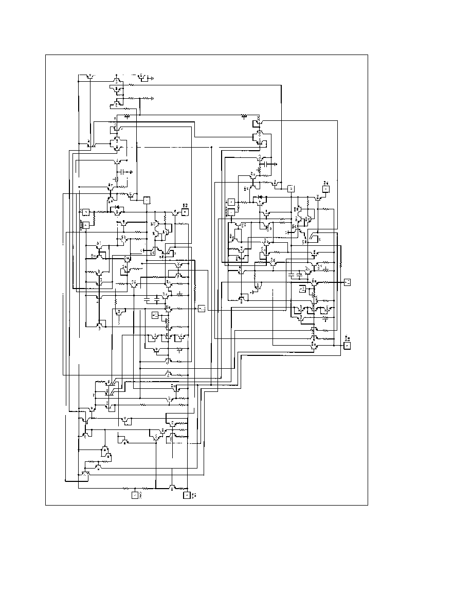
Equivalent Schematic
TL H 5129 ≠ 3
4

External Components
(Figure 2)
Components
Comments
1 R1 R2
Sets voltage gain
R5 R4
A
V
j
1
a
R
R1
for one channel
A
V
e
1
a
R
R5
for the other
Where R' is the equivalent resistance
of R2 in parallel with an internal 10k
resistor
R
e
10k
R2
R2
a
10k
If R2 m 10k then
A
V
j
1
a
R2
R1
2 R3
Adjusts output symmetry for maximum
power output
3 R
O
C
O
Works to stabilize internal output
stage Necessary for stability C
O
should be ceramic disc or equivalently
good high frequency capacitor
4 C1 C9
Input coupling capacitor Low
frequency pole set by
F
L
1
e
1
2
q
Z (non-inverting) C1
Decreasing capacitor value will also
increase noise
Components
Comments
5 C4 C5
Bootstrap capacitors used to increase
drive to output stage
6 C3
Improves power supply rejection
Increasing C3 increases turn-on delay
(approximately 2 ms per mF)
7 C2 C6
Inverting input DC decouple Low
frequency pole
F
L
2
e
1
2
q
Z(inverting)C2
Z (inverting)
10 kX
8 C
C
Output coupling capacitor Isolates
pins 10 and 8 from load Low
frequency pole
F
L
3
e
1
2
q
R
L
C
C
9 C
S
Power supply filtering
Typical Applications
(Continued)
TL H 5129 ≠ 4
FIGURE 2 10W Channel Stereo Amplifier Application and Test Circuit
5