TL H 5680
LM131ALM131
LM231ALM231
LM331ALM331
Precision
Voltage-to-Frequency
Converters
December 1994
LM131A LM131 LM231A LM231 LM331A LM331
Precision Voltage-to-Frequency Converters
General Description
The LM131 LM231 LM331 family of voltage-to-frequency
converters are ideally suited for use in simple low-cost cir-
cuits for analog-to-digital conversion precision frequency-
to-voltage conversion long-term integration linear frequen-
cy modulation or demodulation and many other functions
The output when used as a voltage-to-frequency converter
is a pulse train at a frequency precisely proportional to the
applied input voltage Thus it provides all the inherent ad-
vantages of the voltage-to-frequency conversion tech-
niques and is easy to apply in all standard voltage-to-fre-
quency converter applications
Further
the LM131A
LM231A LM331A attains a new high level of accuracy ver-
sus temperature which could only be attained with expen-
sive voltage-to-frequency modules Additionally the LM131
is ideally suited for use in digital systems at low power sup-
ply voltages and can provide low-cost analog-to-digital con-
version in microprocessor-controlled systems And the fre-
quency from a battery powered voltage-to-frequency con-
verter can be easily channeled through a simple photoisola-
tor to provide isolation against high common mode levels
The LM131 LM231 LM331 utilizes a new temperature-
compensated band-gap reference circuit to provide excel-
lent accuracy over the full operating temperature range at
power supplies as low as 4 0V The precision timer circuit
has low bias currents without degrading the quick response
necessary for 100 kHz voltage-to-frequency conversion
And the output is capable of driving 3 TTL loads or a high
voltage output up to 40V yet is short-circuit-proof against
V
CC
Features
Y
Guaranteed linearity 0 01% max
Y
Improved performance in existing voltage-to-frequency
conversion applications
Y
Split or single supply operation
Y
Operates on single 5V supply
Y
Pulse output compatible with all logic forms
Y
Excellent temperature stability
g
50 ppm C max
Y
Low power dissipation 15 mW typical at 5V
Y
Wide dynamic range 100 dB min at 10 kHz full scale
frequency
Y
Wide range of full scale frequency 1 Hz to 100 kHz
Y
Low cost
Typical Applications
TL H 5680 � 1
Use stable components with low temperature coefficients See Typical Applications section
f
OUT
e
V
IN
2 09 V
R
S
R
L
1
R
t
C
t
0 1mF or 1mF See ``Principles of Operation ''
FIGURE 1 Simple Stand-Alone Voltage-to-Frequency Converter
with
g
0 03% Typical Linearity (f
e
10 Hz to 11 kHz)
C1995 National Semiconductor Corporation
RRD-B30M115 Printed in U S A

Absolute Maximum Ratings
(Note 1)
If Military Aerospace specified devices are required please contact the National Semiconductor Sales Office
Distributors for availability and specifications
LM131A LM131
LM231A LM231
LM331A LM331
Supply Voltage
40V
40V
40V
Output Short Circuit to Ground
Continuous
Continuous
Continuous
Output Short Circuit to V
CC
Continuous
Continuous
Continuous
Input Voltage
b
0 2V to
a
V
S
b
0 2V to
a
V
S
b
0 2V to
a
V
S
T
MIN
T
MAX
T
MIN
T
MAX
T
MIN
T
MAX
Operating Ambient Temperature Range
b
55 C to
a
125 C
b
25 C to
a
85 C
0 C to
a
70 C
Power Dissipation (P
D
at 25 C)
and Thermal Resistance (i
jA
)
(H Package) P
D
670 mW
i
jA
150 C W
(N Package) P
D
1 25W
1 25W
i
jA
100 C W
100 C W
(M Package) P
D
1 25W
i
JA
85 C W
Lead Temperature (Soldering 10 sec )
Dual-In-Line Package (Plastic)
260 C
260 C
260 C
Metal Can Package (TO-5)
260 C
ESD Susceptibility (Note 4)
Metal Can Package (TO-5)
2000V
Other Packages
500V
500V
Electrical Characteristics
T
A
e
25 C unless otherwise specified (Note 2)
Parameter
Conditions
Min
Typ
Max
Units
VFC Non-Linearity (Note 3)
4 5V
s
V
S
s
20V
g
0 003
g
0 01
% Full-
Scale
T
MIN
s
T
A
s
T
MAX
g
0 006
g
0 02
% Full-
Scale
VFC Non-Linearity
V
S
e
15V f
e
10 Hz to 11 kHz
g
0 024
g
0 14
%Full-
In Circuit of
Figure 1
Scale
Conversion Accuracy Scale Factor (Gain)
V
IN
e b
10V R
S
e
14 kX
LM131 LM131A LM231 LM231A
0 95
1 00
1 05
kHz V
LM331 LM331A
0 90
1 00
1 10
kHz V
Temperature Stability of Gain
T
MIN
s
T
A
s
T
MAX
4 5V
s
V
S
s
20V
LM131 LM231 LM331
g
30
g
150
ppm C
LM131A LM231A LM331A
g
20
g
50
ppm C
Change of Gain with V
S
4 5V
s
V
S
s
10V
0 01
0 1
% V
10V
s
V
S
s
40V
0 006
0 06
% V
Rated Full-Scale Frequency
V
IN
e b
10V
10 0
kHz
Gain Stability vs Time
T
MIN
s
T
A
s
T
MAX
g
0 02
% Full-
(1000 Hrs)
Scale
Overrange (Beyond Full-Scale) Frequency
V
IN
e b
11V
10
%
INPUT COMPARATOR
Offset Voltage
g
3
g
10
mV
LM131 LM231 LM331
T
MIN
s
T
A
s
T
MAX
g
4
g
14
mV
LM131A LM231A LM331A
T
MIN
s
T
A
s
T
MAX
g
3
g
10
mV
Bias Current
b
80
b
300
nA
Offset Current
g
8
g
100
nA
Common-Mode Range
T
MIN
s
T
A
s
T
MAX
b
0 2
V
CC
b
2 0
V
2

Electrical Characteristics
T
A
e
25 C unless otherwise specified (Note 2) (Continued)
Parameter
Conditions
Min
Typ
Max
Units
TIMER
Timer Threshold Voltage Pin 5
0 63
0 667
0 70
c
V
S
Input Bias Current Pin 5
V
S
e
15V
All Devices
0V
s
V
PIN 5
s
9 9V
g
10
g
100
nA
LM131 LM231 LM331
V
PIN 5
e
10V
200
1000
nA
LM131A LM231A LM331A
V
PIN 5
e
10V
200
500
nA
V
SAT PIN 5
(Reset)
I
e
5 mA
0 22
0 5
V
CURRENT SOURCE (Pin 1)
Output Current
R
S
e
14 kX V
PIN 1
e
0
LM131 LM131A LM231 LM231A
126
135
144
m
A
LM331 LM331A
116
136
156
m
A
Change with Voltage
0V
s
V
PIN 1
s
10V
0 2
1 0
m
A
Current Source OFF Leakage
LM131 LM131A
0 01
1 0
nA
LM231 LM231A LM331 LM331A
0 02
10 0
nA
All Devices
T
A
e
T
MAX
2 0
50 0
nA
Operating Range of Current (Typical)
(10 to 500)
m
A
REFERENCE VOLTAGE (Pin 2)
LM131 LM131A LM231 LM231A
1 76
1 89
2 02
V
DC
LM331 LM331A
1 70
1 89
2 08
V
DC
Stability vs Temperature
g
60
ppm C
Stability vs Time 1000 Hours
g
0 1
%
LOGIC OUTPUT (Pin 3)
V
SAT
I
e
5 mA
0 15
0 50
V
I
e
3 2 mA (2 TTL Loads) T
MIN
s
T
A
s
T
MAX
0 10
0 40
V
OFF Leakage
g
0 05
1 0
m
A
SUPPLY CURRENT
LM131 LM131A LM231
V
S
e
5V
2 0
3 0
4 0
mA
LM231A
V
S
e
40V
2 5
4 0
6 0
mA
LM331 LM331A
V
S
e
5V
1 5
3 0
6 0
mA
V
S
e
40V
2 0
4 0
8 0
mA
Note 1
Absolute Maximum Ratings indicate limits beyond which damage to the device may occur DC and AC electrical specifications do not apply when operating
the device beyond its specified operating conditions
Note 2
All specifications apply in the circuit of
Figure 3 with 4 0V
s
V
S
s
40V unless otherwise noted
Note 3
Nonlinearity is defined as the deviation of f
OUT
from V
IN
c
(10 kHz
b
10 V
DC
) when the circuit has been trimmed for zero error at 10 Hz and at 10 kHz
over the frequency range 1 Hz to 11 kHz For the timing capacitor C
T
use NPO ceramic Teflon
or polystyrene
Note 4
Human body model 100 pF discharged through a 1 5 kX resistor
3

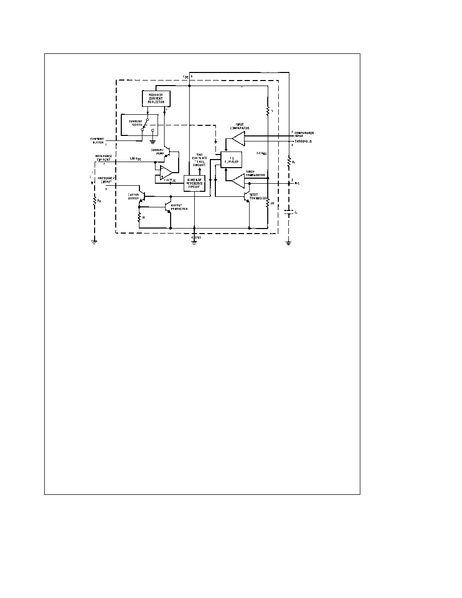
Functional Block Diagram
TL H 5680 � 2
Pin numbers apply to 8-pin packages only See connection diagram for LM231WM pin numbers
FIGURE 1a
Teflon
registered trademark of DuPont
4

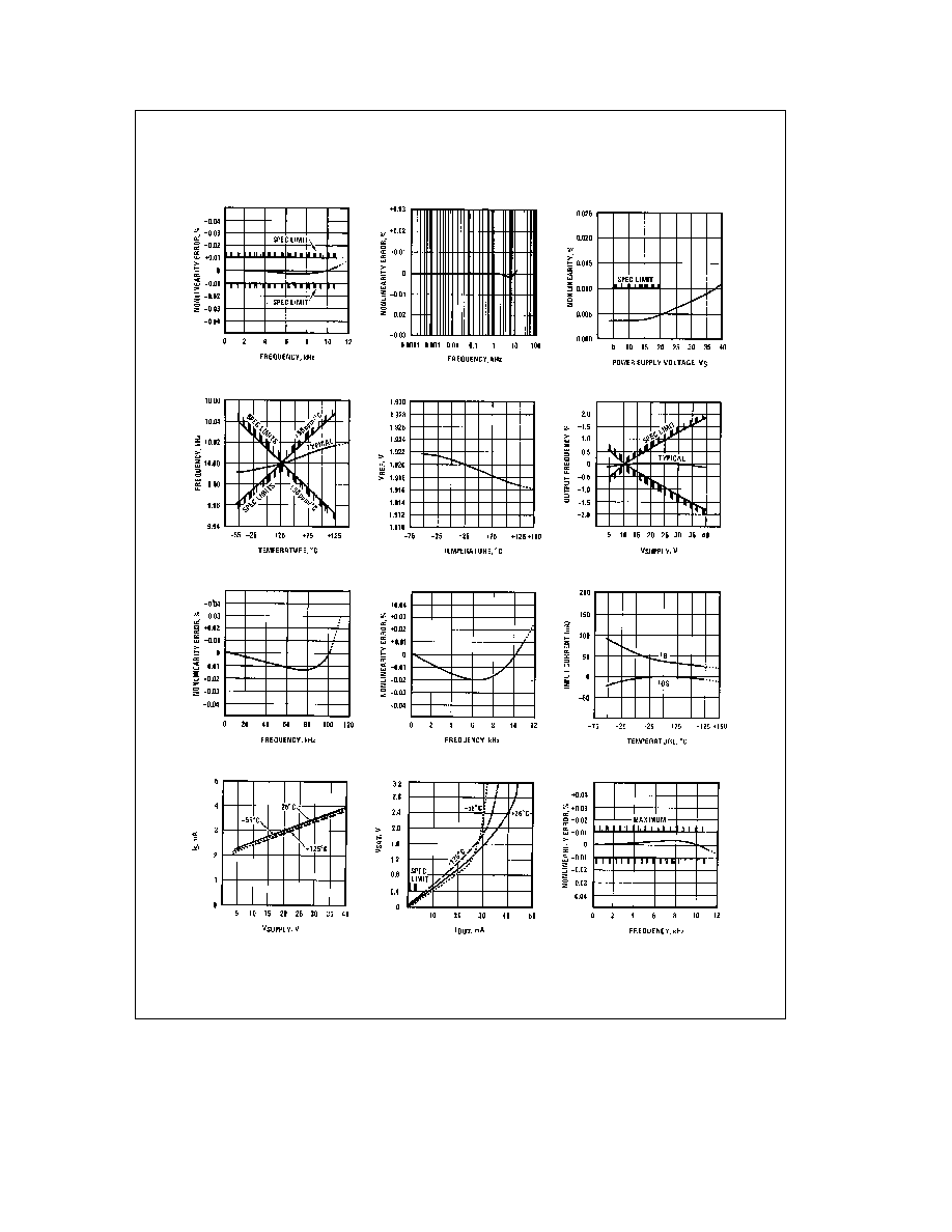
Typical Performance Characteristics
(All electrical characteristics apply for the circuit of
Figure 3 unless otherwise noted )
Nonlinearity Error LM131
Family as Precision V-to-F
Converter (
Figure 3 )
Nonlinearity Error LM131
Family
Nonlinearity vs Power Supply
Voltage
Frequency vs Temperature
LM131A
V
REF
vs Temperature
LM131A
Output Frequency vs
V
SUPPLY
100 kHz Nonlinearity Error
LM131 Family (
Figure 4 )
Nonlinearity Error LM131
(
Figure 1 )
Input Current (Pins 6 7) vs
Temperature
Power Drain vs V
SUPPLY
Output Saturation Voltage vs
I
OUT
(Pin 3)
Nonlinearity Error Precision
F-to-V Converter (
Figure 6 )
TL H 5680 � 3
5

Typical Applications
(Continued)
PRINCIPLES OF OPERATION OF A SIMPLIFIED
VOLTAGE-TO-FREQUENCY CONVERTER
The LM131 is a monolithic circuit designed for accuracy and
versatile operation when applied as a voltage-to-frequency
(V-to-F) converter or as a frequency-to-voltage (F-to-V) con-
verter A simplified block diagram of the LM131 is shown in
Figure 2 and consists of a switched current source input
comparator and 1-shot timer
The operation of these blocks is best understood by going
through the operating cycle of the basic V-to-F converter
Figure 2 which consists of the simplified block diagram of
the LM131 and the various resistors and capacitors con-
nected to it
The voltage comparator compares a positive input voltage
V1 at pin 7 to the voltage V
x
at pin 6 If V1 is greater the
comparator will trigger the 1-shot timer The output of the
timer will turn ON both the frequency output transistor and
the switched current source for a period t
e
1 1 R
t
C
t
During
this period the current i will flow out of the switched current
source and provide a fixed amount of charge Q
e
i
c
t into
the capacitor C
L
This will normally charge V
x
up to a higher
level than V1 At the end of the timing period the current i
will turn OFF and the timer will reset itself
Now there is no current flowing from pin 1 and the capaci-
tor C
L
will be gradually discharged by R
L
until V
x
falls to the
level of V1 Then the comparator will trigger the timer and
start another cycle
The current flowing into C
L
is exactly I
AVE
e
i
c
(1 1
c
R
t
C
t
)
c
f and the current flowing out of C
L
is exactly V
x
R
L
j
V
IN
R
L
If V
IN
is doubled the frequency will double to main-
tain this balance Even a simple V-to-F converter can pro-
vide a frequency precisely proportional to its input voltage
over a wide range of frequencies
TL H 5680 � 4
FIGURE 2 Simplified Block Diagram of Stand-Alone
Voltage-to-Frequency Converter Showing LM131 and
External Components
DETAIL OF OPERATION FUNCTIONAL BLOCK
DIAGRAM (
FIGURE 1a )
The block diagram shows a band gap reference which pro-
vides a stable 1 9 V
DC
output This 1 9 V
DC
is well regulated
over a V
S
range of 3 9V to 40V It also has a flat low tem-
perature coefficient and typically changes less than
%
over a 100 C temperature change
The current pump circuit forces the voltage at pin 2 to be at
1 9V
and causes a current i
e
1 90V R
S
to flow
For
R
s
e
14k i
e
135 mA The precision current reflector pro-
vides a current equal to i to the current switch The current
switch switches the current to pin 1 or to ground depending
on the state of the R
S
flip-flop
The timing function consists of an R
S
flip-flop and a timer
comparator connected to the external R
t
C
t
network When
the input comparator detects a voltage at pin 7 higher than
pin 6 it sets the R
S
flip-flop which turns ON the current
switch and the output driver transistor When the voltage at
pin 5 rises to
V
CC
the timer comparator causes the R
S
flip-flop to reset The reset transistor is then turned ON and
the current switch is turned OFF
However if the input comparator still detects pin 7 higher
than pin 6 when pin 5 crosses
V
CC
the flip-flop will not
be reset and the current at pin 1 will continue to flow in its
attempt to make the voltage at pin 6 higher than pin 7 This
condition will usually apply under start-up conditions or in
the case of an overload voltage at signal input It should be
noted that during this sort of overload the output frequency
will be 0 as soon as the signal is restored to the working
range the output frequency will be resumed
The output driver transistor acts to saturate pin 3 with an
ON resistance of about 50X In case of overvoltage the
output current is actively limited to less than 50 mA
The voltage at pin 2 is regulated at 1 90 V
DC
for all values of
i between 10 mA to 500 mA It can be used as a voltage
reference for other components but care must be taken to
ensure that current is not taken from it which could reduce
the accuracy of the converter
PRINCIPLES OF OPERATION OF BASIC VOLTAGE-
TO-FREQUENCY CONVERTER (
FIGURE 1 )
The simple stand-alone V-to-F converter shown in
Figure 1
includes all the basic circuitry of
Figure 2 plus a few compo-
nents for improved performance
A resistor R
IN
e
100 kX
g
10% has been added in the path
to pin 7 so that the bias current at pin 7 (
b
80 nA typical)
will cancel the effect of the bias current at pin 6 and help
provide minimum frequency offset
The resistance R
S
at pin 2 is made up of a 12 kX fixed
resistor plus a 5 kX (cermet preferably) gain adjust rheo-
stat The function of this adjustment is to trim out the gain
tolerance of the LM131 and the tolerance of R
t
R
L
and C
t
6

Typical Applications
(Continued)
For best results all the components should be stable low-
temperature-coefficient components such as metal-film re-
sistors The capacitor should have low dielectric absorption
depending on the temperature characteristics desired NPO
ceramic polystyrene Teflon or polypropylene are best
suited
A capacitor C
IN
is added from pin 7 to ground to act as a
filter for V
IN
A value of 0 01 mF to 0 1 mF will be adequate in
most cases however in cases where better filtering is re-
quired a 1 mF capacitor can be used When the RC time
constants are matched at pin 6 and pin 7 a voltage step at
V
IN
will cause a step change in f
OUT
If C
IN
is much less
than C
L
a step at V
IN
may cause f
OUT
to stop momentarily
A 47X resistor in series with the 1 mF C
L
is added to give
hysteresis effect which helps the input comparator provide
the excellent linearity (0 03% typical)
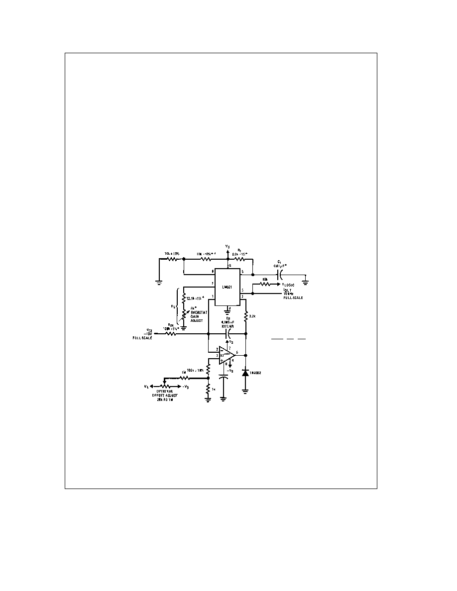
DETAIL OF OPERATION OF PRECISION V-TO-F
CONVERTER
(
FIGURE 3 )
In this circuit integration is performed by using a conven-
tional operational amplifier and feedback capacitor C
F
When the integrator's output crosses the nominal threshold
level at pin 6 of the LM131 the timing cycle is initiated
The average current fed into the op amp's summing point
(pin 2) is i
c
(1 1 R
t
C
t
)
c
f which is perfectly balanced with
b
V
IN
R
IN
In this circuit the voltage offset of the LM131
input comparator does not affect the offset or accuracy of
the V-to-F converter as it does in the stand-alone V-to-F
converter nor does the LM131 bias current or offset cur-
rent Instead the offset voltage and offset current of the
operational amplifier are the only limits on how small the
signal can be accurately converted Since op amps with
voltage offset well below 1 mV and offset currents well be-
low 2 nA are available at low cost this circuit is recommend-
ed for best accuracy for small signals This circuit also re-
sponds immediately to any change of input signal (which a
stand-alone circuit does not) so that the output frequency
will be an accurate representation of V
IN
as quickly as 2
output pulses' spacing can be measured
In the precision mode excellent linearity is obtained be-
cause the current source (pin 1) is always at ground poten-
tial and that voltage does not vary with V
IN
or f
OUT
(In the
stand-alone V-to-F converter a major cause of non-linearity
is the output impedance at pin 1 which causes i to change
as a function of V
IN
)
The circuit of
Figure 4 operates in the same way as Figure 3
but with the necessary changes for high speed operation
f
OUT
e
b
V
IN
2 09 V
R
S
R
IN
1
R
t
C
t
TL H 5680 � 5
Use stable components with low temperature coefficients See Typical Applications section
This resistor can be 5 kX or 10 kX for V
S
e
8V to 22V but must be 10 kX for V
S
e
4 5V to 8V
Use low offset voltage and low offset current op amps for A1 recommended types LM108 LM308A LF411A
FIGURE 3 Standard Test Circuit and Applications Circuit Precision Voltage-to-Frequency Converter
7

Typical Applications
(Continued)
DETAILS OF OPERATION FREQUENCY-TO-
VOLTAGE CONVERTERS
(FIGURES 5 AND 6 )
In these applications a pulse input at f
IN
is differentiated by
a C-R network and the negative-going edge at pin 6 causes
the input comparator to trigger the timer circuit Just as with
a V-to-F converter the average current flowing out of pin 1
is I
AVERAGE
e
i
c
(1 1 R
t
C
t
)
c
f
In the simple circuit of
FIGURE 5 this current is filtered in
the network R
L
e
100 kX and 1 mF The ripple will be less
than 10 mV peak but the response will be slow with a
0 1 second time constant and settling of 0 7 second to
0 1% accuracy
In the precision circuit an operational amplifier provides a
buffered output and also acts as a 2-pole filter The ripple
will be less than 5 mV peak for all frequencies above 1 kHz
and the response time will be much quicker than in
Figure 5
However for input frequencies below 200 Hz this circuit will
have worse ripple than
Figure 5 The engineering of the filter
time-constants to get adequate response and small enough
ripple simply requires a study of the compromises to be
made Inherently V-to-F converter response can be fast
but F-to-V response can not
TL H 5680 � 6
Use stable components with low temperature coefficients
See Typical Applications section
This resistor can be 5 kX or 10 kX for V
S
e
8V to 22V
but must be 10 kX for V
S
e
4 5V to 8V
Use low offset voltage and low offset current op amps for A1
recommended types LF411A or LF356
FIGURE 4 Precision Voltage-to-Frequency Converter
100 kHz Full-Scale
g
0 03% Non-Linearity
TL H 5680 � 7
V
OUT
e
f
IN
c
2 09V
c
R
L
R
S
c
(R
t
C
t
)
Use stable components with low temperature coefficients
FIGURE 5 Simple Frequency-to-Voltage Converter
10 kHz Full-Scale
g
0 06% Non-Linearity
V
OUT
e b
f
IN
c
2 09V
c
R
F
R
S
c
(R
t
C
t
)
TL H 5680 � 8
SELECT Rx
e
(V
S
b
2V)
0 2 mA
Use stable components with low temperature coefficients
FIGURE 6 Precision Frequency-to-Voltage Converter
10 kHz Full-Scale with 2-Pole Filter
g
0 01%
Non-Linearity Maximum
8

Typical Applications
(Continued)
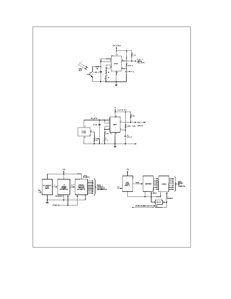
Light Intensity to Frequency Converter
TL H 5680 � 9
L14F-1 L14G-1 or L14H-1 photo transistor (General Electric Co ) or similar
Temperature to Frequency Converter
TL H 5680 � 10
Long-Term Digital Integrator Using VFC
TL H 5680 � 11
Basic Analog-to-Digital Converter Using
Voltage-to-Frequency Converter
TL H 5680 � 12
9

Typical Applications
(Continued)
Analog-to-Digital Converter with Microprocessor
TL H 5680 � 13
Remote Voltage-to-Frequency Converter with 2-Wire Transmitter and Receiver
TL H 5680 � 14
Voltage-to-Frequency Converter with Square-Wave Output Using
d
2 Flip-Flop
TL H 5680 � 15
Voltage-to-Frequency Converter with Isolators
TL H 5680 � 16
10

Typical Applications
(Continued)
Voltage-to-Frequency Converter with Isolators
TL H 5680 � 17
Voltage-to-Frequency Converter with Isolators
TL H 5680 � 18
Voltage-to-Frequency Converter with Isolators
TL H 5680 � 19
11

Connection Diagrams
Metal Can Package
TL H 5680 � 20
Note
Metal case is connected to pin 4 (GND )
Order Number LM131H 883 or LM131AH 883
See NS Package Number H08C
Dual-In-Line Package
TL H 5680 � 21
Order Number LM231AN LM231N LM331AN
or LM331N
See NS Package Number N08E
Small-Outline Package
TL H 5680 � 24
Top View
Order Number LM231WM
See NS Package Number M14B
12

Schematic Diagram
TL H 5680 � 22
13

14

Physical Dimensions
inches (millimeters)
Metal Can Package (H)
Order Number LM131H 883 or LM131AH 883
NS Package H08C
14-Pin Small Outline Package (M)
Order Number LM231WM
NS Package M14B
15

LM131ALM131
LM231ALM231
LM331ALM331
Precision
Voltage-to-Frequency
Converters
Physical Dimensions
inches (millimeters) (Continued)
Dual-In-Line Package (N)
Order Number LM231AN LM231N LM331AN or LM331N
NS package N08E
LIFE SUPPORT POLICY
NATIONAL'S PRODUCTS ARE NOT AUTHORIZED FOR USE AS CRITICAL COMPONENTS IN LIFE SUPPORT
DEVICES OR SYSTEMS WITHOUT THE EXPRESS WRITTEN APPROVAL OF THE PRESIDENT OF NATIONAL
SEMICONDUCTOR CORPORATION As used herein
1 Life support devices or systems are devices or
2 A critical component is any component of a life
systems which (a) are intended for surgical implant
support device or system whose failure to perform can
into the body or (b) support or sustain life and whose
be reasonably expected to cause the failure of the life
failure to perform when properly used in accordance
support device or system or to affect its safety or
with instructions for use provided in the labeling can
effectiveness
be reasonably expected to result in a significant injury
to the user
National Semiconductor
National Semiconductor
National Semiconductor
National Semiconductor
Corporation
Europe
Hong Kong Ltd
Japan Ltd
1111 West Bardin Road
Fax (a49) 0-180-530 85 86
13th Floor Straight Block
Tel 81-043-299-2309
Arlington TX 76017
Email cnjwge tevm2 nsc com
Ocean Centre 5 Canton Rd
Fax 81-043-299-2408
Tel 1(800) 272-9959
Deutsch Tel (a49) 0-180-530 85 85
Tsimshatsui Kowloon
Fax 1(800) 737-7018
English
Tel (a49) 0-180-532 78 32
Hong Kong
Fran ais Tel (a49) 0-180-532 93 58
Tel (852) 2737-1600
Italiano
Tel (a49) 0-180-534 16 80
Fax (852) 2736-9960
National does not assume any responsibility for use of any circuitry described no circuit patent licenses are implied and National reserves the right at any time without notice to change said circuitry and specifications


