LMX2324
PLLatinum
TM
2.0 GHz Frequency Synthesizer for RF
Personal Communications
General Description
The LMX2324 is a high performance frequency synthesizer
with integrated 32/33 dual modulus prescaler designed for
RF operation up to 2.0 GHz. Using a proprietary digital
phase locked loop technique, the LMX2324's linear phase
detector characteristics can generate very stable, low noise
control signals for UHF and VHF voltage controlled oscilla-
tors.
Serial data is transferred into the LMX2324 via a three-line
MICROWIRE
TM
interface (Data, LE, Clock). Supply voltage
range is from 2.7V to 5.5V. The LMX2324 features very low
current consumption, typically 3.5 mA at 3V. The charge
pump provides 4 mA output current.
The LMX2324 is manufactured using National's ABiC V
BiCMOS process and is packaged in a 16-pin TSSOP and a
16-pin Chip Scale Package (CSP).
Features
n
RF operation up to 2.0 GHz
n
2.7V to 5.5V operation
n
Low current consumption: I
CC
= 3.5 mA (typ) at V
CC
=
3.0V
n
Dual modulus prescaler: 32/33
n
Internal balanced, low leakage charge pump
Applications
n
Cellular telephone systems (GSM, NADC, CDMA, PDC)
n
Personal wireless communications (DCS-1800, DECT,
CT-1+)
n
Wireless local area networks (WLANs)
n
Other wireless communication systems
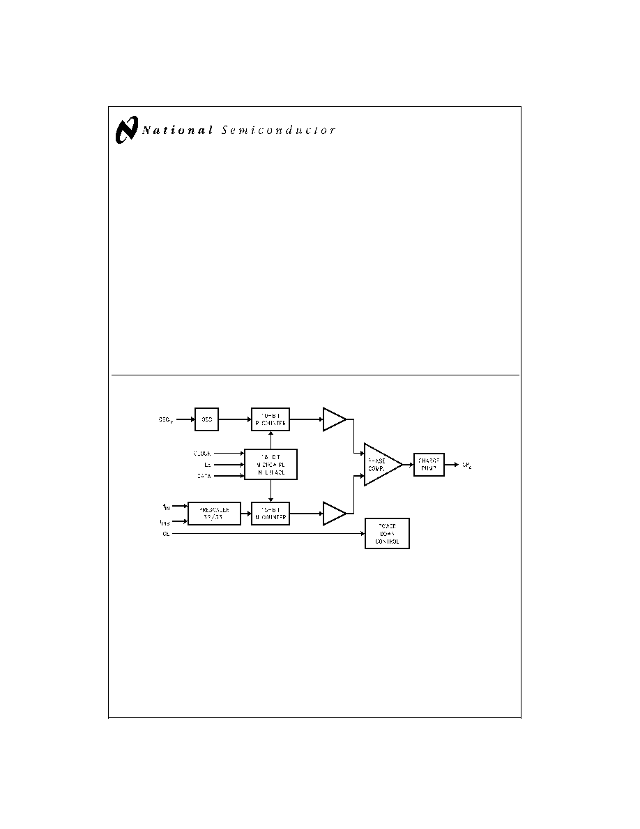
Functional Block Diagram
TRI-STATE
�
is a registered trademark of National Semiconductor Corporation.
MICROWIRE
TM
and PLLatinum
TM
are trademarks of National Semiconductor Corporation.
DS101030-1
PRELIMINARY
November 1999
LMX2324
PLLatinum
2.0
GHz
Frequency
Synthesizer
for
RF
Personal
Communications
� 1999 National Semiconductor Corporation
DS101030
www.national.com
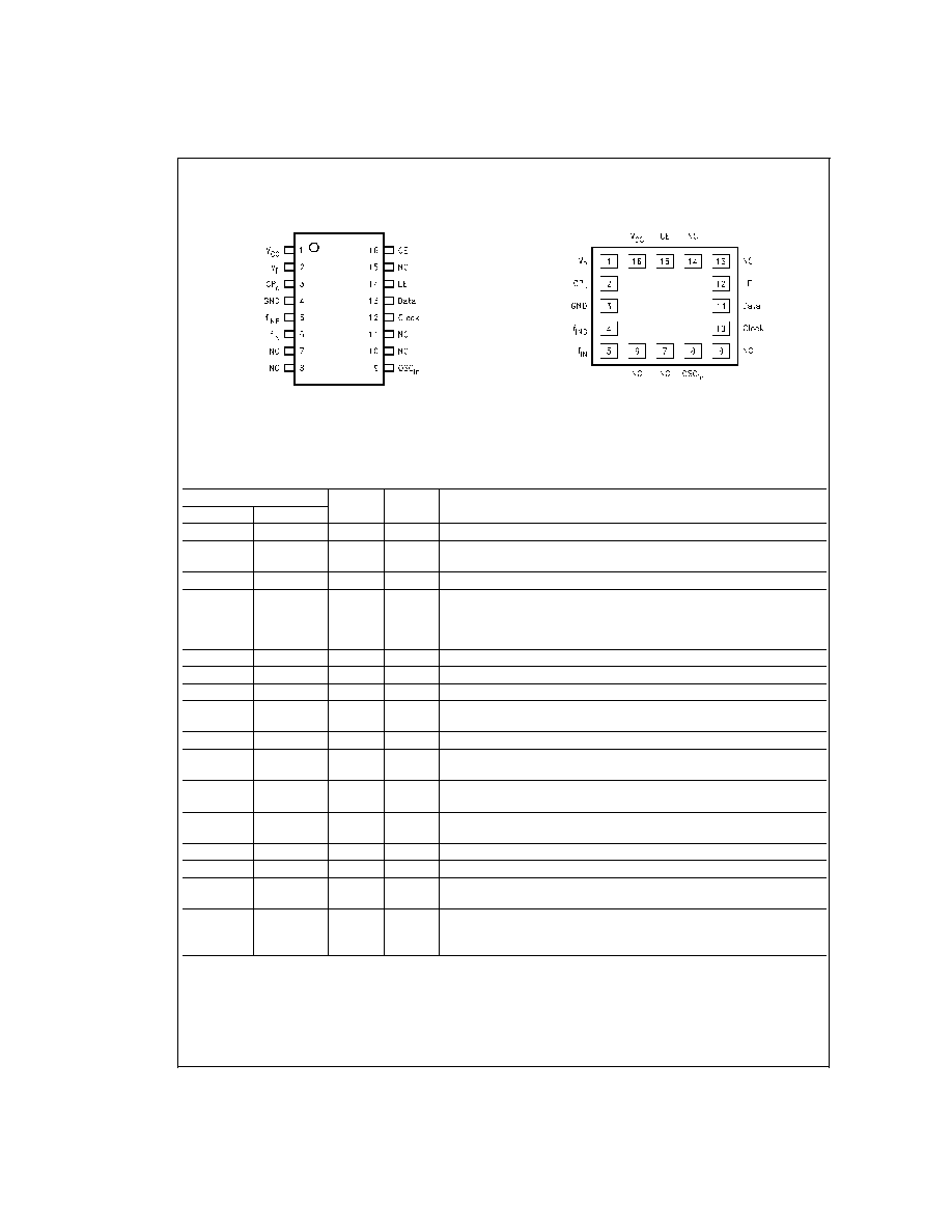
Connection Diagrams
Pin Descriptions
Pin No.
Pin
Name
I/O
Description
TSSOP16
CSP16
2
1
V
P
--
Power supply for charge pump. Must be
V
CC
3
2
CP
o
O
Internal charge pump output. For connection to a loop filter for driving the
voltage control input of an external oscillator.
4
3
GND
--
Ground.
5
4
f
INB
I
RF prescaler complimentary input. In single-ended mode, a bypass
capacitor should be placed as close as possible to this pin and be
connected directly to the ground plane. The LMX2324 can be driven
differentially when the bypass capacitor is omitted.
6
5
f
IN
I
RF prescaler input. Small signal input from the voltage controlled oscillator.
7
6
NC
No Connect
8
7
NC
No Connect
9
8
OSC
in
I
Oscillator input. A CMOS inverting gate input. The input has a V
CC
/2 input
threshold and can be driven from an external CMOS or TTL logic gate.
10
9
NC
No Connect
12
10
Clock
I
High impedance CMOS Clock input. Data is clocked in on the rising edge,
into the various counters and registers.
13
11
Data
I
Binary serial data input. Data entered MSB first. LSB is control bit. High
impedance CMOS input.
14
12
LE
I
Load Enable input. When Load Enable transitions HIGH, data is loaded
into either the N or R register (control bit dependent). See timing diagram.
15
13
NC
No Connect
11
14
NC
No Connect
16
15
CE
I
CHIP Enable. A LOW on CE powers down the device asynchronously and
will TRI-STATE
�
the charge pump output.
1
16
V
CC
I
Power supply voltage input. Input may range from 2.7V to 5.5V. Bypass
capacitors should be placed as close as possible to this pin and be
connected directly to the ground plane.
TSSOP 16-Pin Package
DS101030-2
Order Number LMX2324TM, LM2324TMX
See NS Package Number MTC16
CSP 16-Pin Package
DS101030-3
Top View
Order Number LMX2324SLBX
See NS Package Number SLB16A
LMX2324
www.national.com
2
Absolute Maximum Ratings
(Note 1)
If Military/Aerospace specified devices are required,
please contact the National Semiconductor Sales Office/
Distributors for availability and specifications.
Power Supply Voltage (V
CC
)
-0.3V to 6.5V
Power Supply for Charge Pump (V
P
)
V
CC
to 6.5V
Voltage on Any Pin with
GND = 0V (V
I
)
-0.3V to V
CC
+ 0.3V
Storage Temperature Range (T
S
)
-65�C to +150�C
Lead Temperature (solder, 4 sec.) (T
L
)
+260�C
ESD - Human Body Model (Note 2)
2 kV
Recommended Operating
Conditions
(Note 1)
Power Supply Voltage (V
CC
)
2.7V to 5.5V
Power Supply for Charge Pump (V
P
)
V
CC
to 5.5V
Operating Temperature (T
A
)
-40�C to +85�C
Note 1: Absolute Maximum Ratings indicate limits beyond which damage to
the device may occur. Recommended Operating Conditions indicate condi-
tions for which the device is intended to be functional, but do not guarantee
specific performance limits. For guaranteed specifications and test condi-
tions, see the Electrical Characteristics.
Note 2: This device is a high performance RF integrated circuit and is ESD
sensitive. Handling and assembly of this device should on be done on ESD
protected workstations.
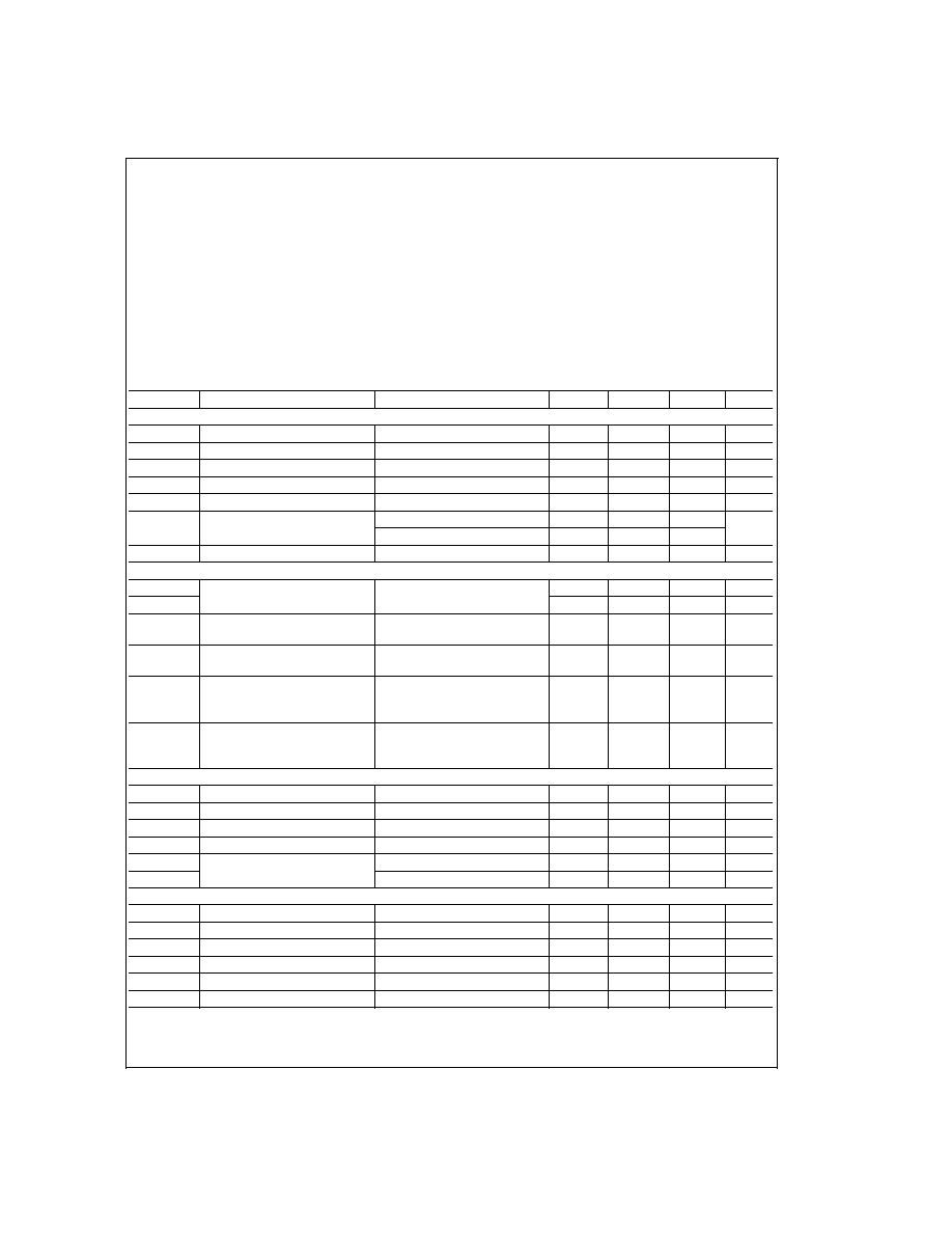
Electrical Characteristics
(V
CC
= 3V, V
P
= 3V; -40�C
<
T
A
<
85�C except as specified).
Symbol
Parameter
Conditions
Min
Typ
Max
Units
GENERAL
I
CC
Power Supply Current
V
CC
= 2.7V to 5.5V
3.5
mA
I
CC
-PWDN
Power Down Current
10
�A
f
IN
f
IN
Operating Frequency
0.1
2.0
GHz
OSC
in
Oscillator Operating Frequency
5
40
MHz
f
PD
Phase Detector Frequency
10
MHz
Pf
IN
Input Sensitivity f
INB
grounded
through a 10 pF capacitor
V
CC
= 3.0V
-15
0
dBm
V
CC
= 5.0V
-10
0
V
OSC
Oscillator Sensitivity
0.4
1.0
V
CC
-0.3
V
PP
CHARGE PUMP
ICP
o-source
Charge Pump Output Current
VCP
o
= V
P
/2
-4.0
mA
ICP
o-sink
4.0
mA
ICP
o-Tri
Charge Pump TRI-STATE
Current
0.5
VCP
o
V
P
- 0.5
T = 25�C
0.1
nA
ICP
o
vs.
VCP
o
Charge Pump Output Current
Variation vs. Voltage (Note 4)
0.5
VCP
o
V
P
- 0.5
T = 25�C
10
%
ICP
o-sink
vs.
ICP
o-source
Charge Pump Output Current
Sink vs. Source Mismatch
(Note 4)
VCP
o
= V
P
/2
T = 25�C
5
%
ICP
o
vs. T
Charge Pump Output Current
Magnitude Variation vs.
Temperature (Note 4)
VCP
o
= V
P
/2
-40�C
T
+85�C
10
%
DIGITAL INTERFACE (DATA, CLK, LE, CE)
V
IH
High-Level Input Voltage
(Note 3)
0.8 V
CC
V
V
IL
Low-Level Input Voltage
(Note 3)
0.2 V
CC
V
I
IH
High-Level Input Current
V
IH
= V
CC
= 5.5V
-1.0
1.0
�A
I
IL
Low-Level Input Current
V
IL
= 0, V
CC
= 5.5V
-1.0
1.0
�A
I
IH
Oscillator Input Current
V
IH
= V
CC
= 5.5V
100
�A
I
IL
V
IL
= 0, V
CC
= 5.5V
-100
�A
MICROWIRE TIMING
t
CS
Data to Clock Set Up Time
See Data Input Timing
50
ns
t
CH
Data to Clock Hold Time
See Data Input Timing
10
ns
t
CWH
Clock Pulse Width High
See Data Input Timing
50
ns
t
CWL
Clock Pulse Width Low
See Data Input Timing
50
ns
t
ES
Clock to Enable Set Up Time
See Data Input Timing
50
ns
t
EW
Enable Pulse Width
See Data Input Timing
50
ns
Note 3: Except f
IN
and OSC
in
Note 4: See related equations in charge pump current specification definitions
LMX2324
www.national.com
3

Charge Pump Current Specification Definitions
DS101030-4
I1 = CP sink current at VCP
o
= V
P
-
V
I2 = CP sink current at VCP
o
= V
P
/2
I3 = CP sink current at VCP
o
=
V
I4 = CP source current at VCP
o
= V
P
-
V
I5 = CP source current at VCP
o
= V
P
/2
I6 = CP source current at VCP
o
=
V
V = Voltage offset from positive and negative rails. Dependent on VCO tuning range relative to V
P
and ground. Typical values are between 0.5V and 1.0V.
1. ICP
o
vs. VCP
o
= Charge Pump Output Current magnitude variation vs. Voltage =
[
1
/
2
*
{|I1| - |I3|}]/[
1
/
2
*
{|I1| + |I3|}]
*
100%
and
[
1
/
2
*
{|I4| - |I6|}]/[
1
/
2
*
{|I4| + |I6|}]
*
100%
2. ICP
o-sink
vs. ICP
o-source
= Charge Pump Output Current Sink vs. Source Mismatch =
[|I2| - |I5|]/[
1
/
2
*
{|I2| + |I5|}]
*
100%
3. ICP
o
vs. T = Charge Pump Output Current magnitude variation vs. Temperature =
[|I2
@
temp| - |I2
@
25�C|]/|I2
@
25�C|
*
100%
and
[|I5
@
temp| - |I5
@
25�C|]/|I5
@
25�C|
*
100%
LMX2324
www.national.com
4

1.0 Functional Description
The basic phase-lock-loop (PLL) configuration consists of a
high-stability crystal reference oscillator, a frequency synthe-
sizer such as the National Semiconductor LMX2324, a volt-
age controlled oscillator (VCO), and a passive loop filter. The
frequency synthesizer includes a phase detector, current
mode charge pump, as well as programmable reference [R]
and feedback [N] frequency dividers. The VCO frequency is
established by dividing the crystal reference signal down via
the R counter to obtain a frequency that sets the comparison
frequency. This reference signal, f
r
, is then presented to the
input of a phase/frequency detector and compared with an-
other signal, f
p
, the feedback signal, which was obtained by
dividing the VCO frequency down by way of the N counter.
The phase/frequency detector's current source outputs
pump charge into the loop filter, which then converts the
charge into the VCO's control voltage. The phase/frequency
comparator's function is to adjust the voltage presented to
the VCO until the feedback signal's frequency (and phase)
match that of the reference signal. When this "phase-locked"
condition exists, the RF VCO's frequency will be N times that
of the comparison frequency, where N is the divider ratio.
1.1 OSCILLATOR
The reference oscillator frequency for the PLL is provided by
an external reference TCXO through the OSC
in
pin. OSC
in
block can operate to 40 MHz with a minimum input sensitivity
of 0.4V
PP
. The inputs have a V
CC
/2 input threshold and can
be driven from an external CMOS or TTL logic gate.
1.2 REFERENCE DIVIDERS (R COUNTER)
The R Counter is clocked through the oscillator block. The
maximum frequency is 40 MHz. The R Counter is a 10 bit
CMOS binary counters with a divide range from 2 to 1,023.
See programming description 2.2.1.
1.3 PROGRAMMABLE DIVIDERS (N COUNTER)
The N counter is clocked by the small signal f
IN
and f
INB
input
pins. The LMX2324 RF N counter is 15 bit integer divider.
The N counter is configured as a 5 bit A Counter and a 10 bit
B Counter, offering a continuous integer divide range from
992 to 32,767. The LMX2324 is capable of operating from
100 MHz to 2.0 GHz with a 32/33 prescaler.
1.3.1 Prescaler
The RF inputs to the prescaler consist of the f
IN
and f
INB
pins
which are the complimentary inputs of a differential pair am-
plifier. The differential f
IN
configuration can operate to 2 GHz
with an input sensitivity of -15 dBm. The input buffer drives
the N counter's ECL D-type flip flops in a dual modulus con-
figuration. A 32/33 prescale ratio is provided for the
LMX2324. The prescaler clocks the subsequent CMOS flip-
flop chain comprising the fully programmable A and B
counters.
1.4 PHASE/FREQUENCY DETECTOR
The phase(/frequency) detector is driven from the N and R
counter outputs. The maximum frequency at the phase de-
tector inputs is 10 MHz. The phase detector outputs control
the charge pumps. The polarity of the pump-up or pump-
down control is programmed using PD_POL, depending on
whether RF VCO characteristics are positive or negative
(see programming description 2.2.2). The phase detector
also receives a feedback signal from the charge pump, in or-
der to eliminate dead zone.
1.5 CHARGE PUMP
The phase detector's current source output pumps charge
into an external loop filter, which then converts the charge
into the VCO's control voltage. The charge pumps steer the
charge pump output, CP
o
, to V
P
(pump-up) or Ground
(pump-down). When locked, CP
o
is primarily in a TRI-STATE
mode with small corrections. The RF charge pump output
current magnitude is set to 4.0 mA. The charge pump output
can also be used to output divider signals as detailed in sec-
tion 2.2.3.
1.6 MICROWIRE SERIAL INTERFACE
The programmable functions are accessed through the
MICROWIRE serial interface. The interface is made of three
functions: clock, data and latch enable (LE). Serial data for
the various counters is clocked in from data on the rising
edge of clock, into the 18-bit shift register. Data is entered
MSB first. The last bit decodes the internal register address.
On the rising edge of LE, data stored in the shift register is
loaded into one of the two appropriate latches (selected by
address bits). A complete programming description is in-
cluded in the following sections.
1.7 POWER CONTROL
The PLL can be power controlled in two ways. The first
method is by setting the CE pin LOW. This asynchronously
powers down the PLL and TRI-STATE the charge pump out-
put, regardless of the PWDN bit status. The second method
is by programming through MICROWIRE, while keeping the
CE HIGH. Programming the PWDN bit in the N register
HIGH (CE=HIGH) will disable the N counter and de-bias the
f
IN
input (to a high impedance state). The R counter function-
ality also becomes disabled. The reference oscillator block
powers down when the power down bit is asserted. The
OSC
in
pin reverts to a high impedance state when this con-
dition exists. Power down forces the charge pump and
phase comparator logic to a TRI-STATE condition. A power
down counter reset function resets both N and R counters.
Upon powering up the N counter resumes counting in "close"
alignment with the R counter (The maximum error is one
prescaler cycle). The MICROWIRE control register remains
active and capable of loading and latching in data during all
of the power down modes.
LMX2324
www.national.com
5