
TL H 12327
LM2406
Monolithic
9
n
s
Triple
CRT
Driver
June 1995
LM2406
Monolithic Triple 9 ns CRT Driver
General Description
The LM2406 is an integrated high voltage CRT driver circuit
designed for use in color monitor applications The IC con-
tains three high input impedance wide band amplifiers
which directly drive the RGB cathodes of a CRT The gain of
each channel is internally set at
b
14 5 and can drive CRT
capacitive loads as well as resistive loads presented by oth-
er applications limited only by the package's power dissipa-
tion
The IC is packaged in an industry standard 11 lead TO-220
molded plastic power package See thermal considerations
on page 4
Features
Y
Output swing capability 50 V
PP
for V
CC
e
80
40 V
PP
for V
CC
e
70
30 V
PP
for V
CC
e
60
Y
Pinout designed for easy PCB layout
Y
1V to 7V input range
Y
Stable with 0 pF � 20 pF capacitive loads
Y
Convenient TO-220 staggered lead style package
Applications
Y
CRT driver for 1024 x 768 (Non-interlaced) and SVGA
display resolution color monitors
Y
Pixel clock frequency up to 80 MHz
Schematic and Connection Diagrams
TL H 12327 � 1
FIGURE 1 Simplified Schematic Diagram (One Channel)
TL H 12327 � 2
Note
Tab is at GND
Top View
C1995 National Semiconductor Corporation
RRD-B30M115 Printed in U S A
Absolute Maximum Ratings
(Notes 1 3)
Supply Voltage V
CC
a
95V
Bias Voltage V
BIAS
a
16V
Input Voltage V
IN
b
0 5V to V
BIAS
a
0 5V
Storage Temperature Range T
STG
b
65 C to
a
150 C
Lead Temperature (Soldering
k
10 sec )
300 C
ESD Tolerance
2 kV
Operating Range
(Note 2)
V
CC
a
60V to
a
85V
V
BIAS
a
8V to
a
15V
V
IN
a
1V to
a
7V
Case Temperature T
CASE
b
20 C to
a
100 C
Do not operate the part without a heat sink
Electrical Characteristics
Unless otherwise noted V
CC
e a
80V V
BIAS
e a
12V V
IN
e a
3 3V C
L
e
8 pF Output
e
40 V
PP
at 1 MHz T
A
e
25 C
Symbol
Parameter
Conditions
LM2406
Units
Min
Typical
Max
I
CC
Supply Current (Per Channel)
No Output Load
18
30
mA
V
OUT
Output Voltage
No Input Signal
45
50
55
V
DC
t
R
Rise Time
10% � 90% f
e
1 MHz
9
nS
t
F
Fall Time
90% � 10% f
e
1 MHz
9
nS
A
V
Voltage Gain
b
13
b
14 5
b
16
V V
LE
Linearity Error
(Note 4)
8
%
D
A
V
Gain Matching
(Note 5)
1 0
dB
Note 1
Absolute Maximum Ratings indicate limits beyond which damage to the device may occur
Note 2
Operating ratings indicate conditions for which the device is functional but do not guarantee specific performance limits For guaranteed specifications and
test conditions see the Electrical Characteristics The guaranteed specifications apply only for the test conditions listed Some performance characteristics may
change when the device is not operated under the listed test conditions
Note 3
All voltages are measured with respect to GND unless otherwise specified
Note 4
Linearity Error is defined as the variation in small signal gain from
a
30V to
a
70V output with a 100 mV AC 10 kHz input signal
Note 5
Calculated value from Voltage Gain test on each channel
Note 6
Input signal V
IN
t
r
t
f
k
2 nS
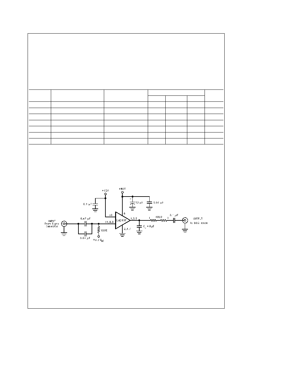
AC Test Circuit
TL H 12327 � 3
Note
8 pF is total load including parasitic capacitance
FIGURE 2 Test Circuit (One Channel)
Figure 2 shows a typical test circuit for evaluation of the LM2406 This circuit is designed to allow testing of the LM2406 in a 50X
environment such as a pulse generator oscilloscope or network analyzer The two series resistors at the output form a 100 1
voltage divider when connected to a 50X load
2
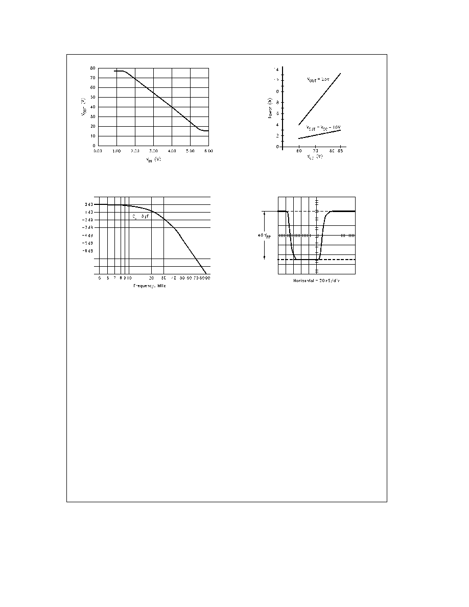
TL H 12327 � 4
FIGURE 3 V
OUT
vs V
IN
TL H 12327 � 5
FIGURE 4 Power Dissipation vs V
CC
TL H 12327 � 6
FIGURE 5 Large Signal Frequency Response
TL H 12327 � 7
FIGURE 6 Pulse Response
Theory of Operation
The LM2406 is a high voltage monolithic triple CRT driver
suitable for VGA and SVGA display applications
The
LM2406 features
a
80V operation and low power dissipa-
tion The part is housed in the industry standard 11-lead
TO-220 molded plastic power package
The circuit diagram of the LM2406 is shown in
Figure 1 Q1
and R2 provide a conversion of input voltage to current
while Q2 acts as a common base or cascode amplifier stage
to drive the load resistor R1 Emitter followers Q3 and Q4
isolate the impedance of R1 from the capacitance of the
CRT cathode and make the circuit relative insensitive to
load capacitance The gain of this circuit is
b
R1 (R2
ll
R3)
and is fixed at
b
14 5 The bandwidth of the circuit is set by
the collector time constant formed by the resistor R1 and
associated capacitance of Q2 Q3 Q4 and stray layout ca-
pacitance Transistor Q6 and resistors R7 and R8 provide
biasing to the output emitter-follower stage to reduce cross-
over distortion at low signal levels while R3 provides a DC
bias offset to match the output level characteristics of the
preamplifier stage
Figure 2 shows a typical test circuit for evaluation of the
LM2406 This circuit is designed to allow testing of the
LM2406 in a 50X environment such as a pulse generator
and a scope or a network analyzer In this test circuit two
resistors in series totaling 4 95 kX form a 100 1 wideband
low capacitance probe when connected to a 50X cable and
load The input signal from the generator is AC coupled to
the base of Q5 while a DC bias of
a
12V is applied to the
base of Q2 (See
Figure 2 )
3
Application Hints
POWER SUPPLY BYPASS
Since the LM2406 is a wide bandwidth amplifier proper
power supply bypassing is critical for optimum performance
Improper power supply bypassing can result in large over-
shoot ringing and oscillation A 0 01 mF capacitor should be
connected as close to the supply pin V
a
as is practical
(preferably less than
from the supply pin) Additionally
a 10 mF � 100 mF electrolytic capacitor should be connected
from the supply pin to ground The electrolytic capacitor
should also be placed reasonably close to the LM2406's
supply pin A 0 1 mF capacitor should be connected from
the bias pin to ground as close as is practical to the
LM2406
The LM2406 is short circuit proof to momentary shorts to
ground (
k
1 sec )
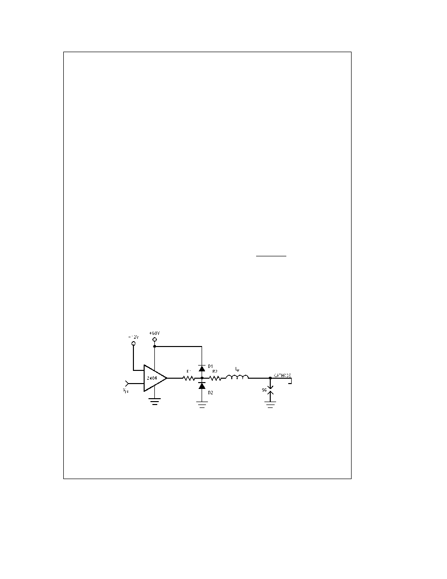
ARC PROTECTION
During normal CRT operation internal arcing may occasion-
ally occur Spark gaps of 200V � 300V at the cathodes will
limit the maximum voltage but to a value that is much high-
er than allowable on the LM2406 This fast high voltage
high energy pulse can damage the LM2406 output stage
The addition of clamp diodes D1 and D2 (as shown in
Fig-
ure 7 ) will help clamp the voltage at the output of the
LM2406 to a safe level The clamp diodes should have a
fast transient response high peak current rating low series
impedance and low shunt capacitance FDH400 or equiva-
lent diodes are recommended Resistor R2 in
Figure 7 limits
the arcover current while R1 limits the current into the
LM2406 and reduces the power dissipation of the output
transistors when the output is stressed beyond the supply
voltage Having large value resistors for R1 and R2 would
be desirable but this has the effect of increasing rise and
fall times
IMPROVING RISE AND FALL TIMES
Because of an emitter follower output stage the rise and fall
times of the LM2406 are relatively insensitive to capacitive
loading However the series resistors R1 and R2 (see
Fig-
ure 7 ) will increase the rise and fall times when driving the
CRT's cathode which appears as a capacitive load The ca-
pacitance at the cathode typically ranges from 8 pF � 12 pF
To improve the rise and fall times at the cathode a small
inductor is often used in series with the output of the amplifi-
er The inductor L
P
in
Figure 7 peaks the amplifiers frequen-
cy response at the cathode thus improving rise and fall
times The inductor value is empirically determined and is
dependent on the load An inductor value of 0 1 mH is a
good starting value Note that peaking the amplifier's fre-
quency response will increase the overshoot
THERMAL CONSIDERATIONS
Power supply current increases as the input signal increas-
es and consequently power dissipation also increases
The LM2406 cannot be used without heat sinking Typical
``average'' power dissipation with the device output voltage
at one half the supply voltage is 2 4W per channel for a total
dissipation of 7 2W package dissipation Under white screen
conditions i e
25V output dissipation increases to 3 5W
per channel or 10 5W total The LM2406 case temperature
must be maintained below 100 C If the maximum expected
ambient temperature is 50 C then a maximum heat sink
thermal resistance can be calculated
R
th
e
100 C
b
50 C
10 5W
e
4 76 C W
This example assumes a typical CRT capacitive load and is
without a resistive load
TYPICAL APPLICATION
A typical application of the LM2406 is shown in
Figure 8
Used in conjunction with an LM1207 a complete video
channel from monitor input to CRT cathode can be
achieved Performance is satisfactory for all applications up
to 1024 x 768 non-interlaced
TL H 12327 � 8
FIGURE 7 One Section of the LM2406 with Arc Protection and Peaking Inductor L
P
4
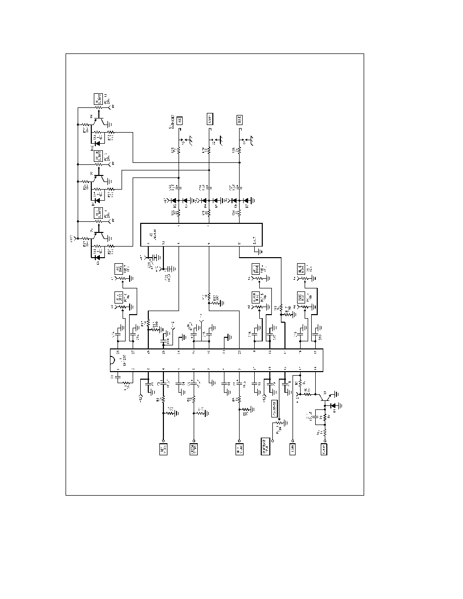
Typical Applications
TLH12327
�
9
Note
Unmarked
capacitors
01
m
F
FIGURE
8
Typical
Application
LM1207
�
LM2406
5

LM2406
Monolithic
9
n
s
Triple
CRT
Driver
Physical Dimensions
inches (millimeters)
11-Lead Molded TO-220
Order Number LM2406
NS Package Number TA11B
LIFE SUPPORT POLICY
NATIONAL'S PRODUCTS ARE NOT AUTHORIZED FOR USE AS CRITICAL COMPONENTS IN LIFE SUPPORT
DEVICES OR SYSTEMS WITHOUT THE EXPRESS WRITTEN APPROVAL OF THE PRESIDENT OF NATIONAL
SEMICONDUCTOR CORPORATION As used herein
1 Life support devices or systems are devices or
2 A critical component is any component of a life
systems which (a) are intended for surgical implant
support device or system whose failure to perform can
into the body or (b) support or sustain life and whose
be reasonably expected to cause the failure of the life
failure to perform when properly used in accordance
support device or system or to affect its safety or
with instructions for use provided in the labeling can
effectiveness
be reasonably expected to result in a significant injury
to the user
National Semiconductor
National Semiconductor
National Semiconductor
National Semiconductor
Corporation
Europe
Hong Kong Ltd
Japan Ltd
1111 West Bardin Road
Fax (a49) 0-180-530 85 86
13th Floor Straight Block
Tel 81-043-299-2309
Arlington TX 76017
Email cnjwge tevm2 nsc com
Ocean Centre 5 Canton Rd
Fax 81-043-299-2408
Tel 1(800) 272-9959
Deutsch Tel (a49) 0-180-530 85 85
Tsimshatsui Kowloon
Fax 1(800) 737-7018
English
Tel (a49) 0-180-532 78 32
Hong Kong
Fran ais Tel (a49) 0-180-532 93 58
Tel (852) 2737-1600
Italiano
Tel (a49) 0-180-534 16 80
Fax (852) 2736-9960
National does not assume any responsibility for use of any circuitry described no circuit patent licenses are implied and National reserves the right at any time without notice to change said circuitry and specifications