LM2426TE
Monolithic Triple Channel 30 MHz DTV Driver
General Description
The LM2426TE is an integrated high voltage CRT driver
circuit designed for use in HDTV applications. The IC con-
tains three high input impedance, wide band amplifiers
which directly drive the RGB cathodes of a CRT. Each
channel has its gain internally set to -53 and can drive CRT
capacitive loads as well as resistive loads present in other
applications, limited only by the package's power dissipation.
The IC is packaged in an industry standard 11-lead TO-220
molded plastic power package designed specifically to meet
high voltage spacing requirements. See Thermal Consider-
ations section.
Features
n
0V to 5V input range
n
Greater than 130V
PP
output swing capability
n
Stable with 0�20 pF capacitive loads and inductive
peaking networks
n
Convenient TO-220 staggered thin lead package style
Applications
n
AC coupled HDTV applications using the 1080i and
720p formats as well as standard NTSC and PAL
formats.
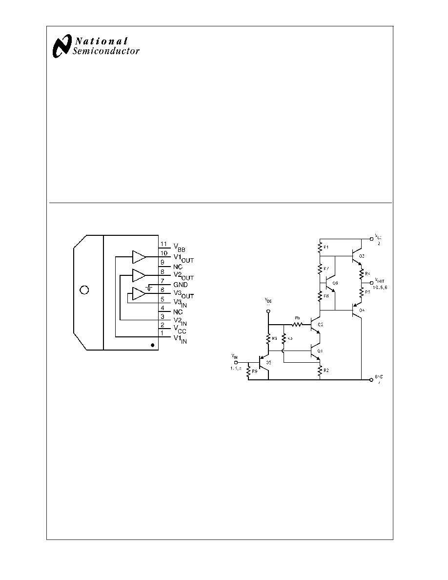
Connection Diagram
Schematic Diagram
20066402
Note: Tab is at GND
Top View
Order Number LM2426TE
FIGURE 1. Simplified Connection and Pinout Diagram
20066401
FIGURE 2. Simplified Schematic Diagram
(One Channel)
May 2003
LM2426TE
Monolithic
T
riple
Channel
30
MHz
DTV
Driver
� 2003 National Semiconductor Corporation
DS200664
www.national.com
Absolute Maximum Ratings
(Notes 1,
3)
If Military/Aerospace specified devices are required,
please contact the National Semiconductor Sales Office/
Distributors for availability and specifications.
Supply Voltage (V
CC
)
+200V
Bias Voltage (V
BB
)
+15V
Input Voltage (V
IN
)
-0.5V to V
BB
+0.5V
Storage Temperature Range (T
STG
)
-65�C to +150�C
Lead Temperature
(Soldering,
<
10 sec.)
300�C
ESD Tolerance,
Human Body Model
2kV
Machine Model
200V
Junction Temperature
150�C
JC
(typ)
2.9�C/W
Operating Ranges
(Note 2)
V
CC
+130V to +180V
V
BB
+7V to +13V
V
IN
+0V to +4V
V
OUT
+15V to +175V
Case Temperature
Refer to Figure 11
Do not operate the part without a heat sink.
Electrical Characteristics
(See Figure 3 for Test Circuit) Unless otherwise noted: V
CC
= +180V, V
BB
= +8V, C
L
= 8pF, T
C
= 50�C. DC Tests: V
IN
=
2.5V
DC
. AC Tests: Output = 110V
PP
(55V - 165V) at 1MHz.
Symbol
Parameter
Conditions
LM2426TE
Units
Min
Typical
Max
I
CC
Supply Current
All Three Channels, No Input Signal,
No Output Load
28
40
mA
I
BB
Bias Current
All Three Channels
15
22
mA
V
OUT, 1
DC Output Voltage
No AC Input Signal, V
IN
= 2.5V
DC
93
98
103
V
DC
V
OUT, 2
DC Output Voltage
No AC Input Signal, V
IN
= 1.2V
DC
160
165
170
V
DC
A
V
DC Voltage Gain
No AC Input Signal
-50
-53
-56
A
V
Gain Matching
(Note 4), No AC Input Signal
1.0
dB
LE
Linearity Error
(Notes 4, 5), No AC Input Signal
8
%
t
R
Rise Time
(Note 6), 10% to 90%
13
ns
t
F
Fall Time
(Note 6), 90% to 10%
13
ns
OS
Overshoot
(Note 6)
7
%
Note 1: Absolute Maximum Ratings indicate limits beyond which damage to the device may occur.
Note 2: Operating ratings indicate conditions for which the device is functional, but do not guarantee specific performance limits. For guaranteed specifications and
test conditions, see the Electrical Characteristics. Datasheet min/max specification limits are guaranteed by design, test, or statistical analysis. The guaranteed
specifications apply only for the test conditions listed. Some performance characteristics may change when the device is not operated under the listed test
conditions.
Note 3: All voltages are measured with respect to GND, unless otherwise specified.
Note 4: Calculated value from Voltage Gain test on each channel.
Note 5: Linearity Error is the variation in DC gain from V
IN
= 1.1V to V
IN
= 3.8V.
Note 6: Input from signal generator: t
r
, t
f
<
1 ns.
LM2426TE
www.national.com
2
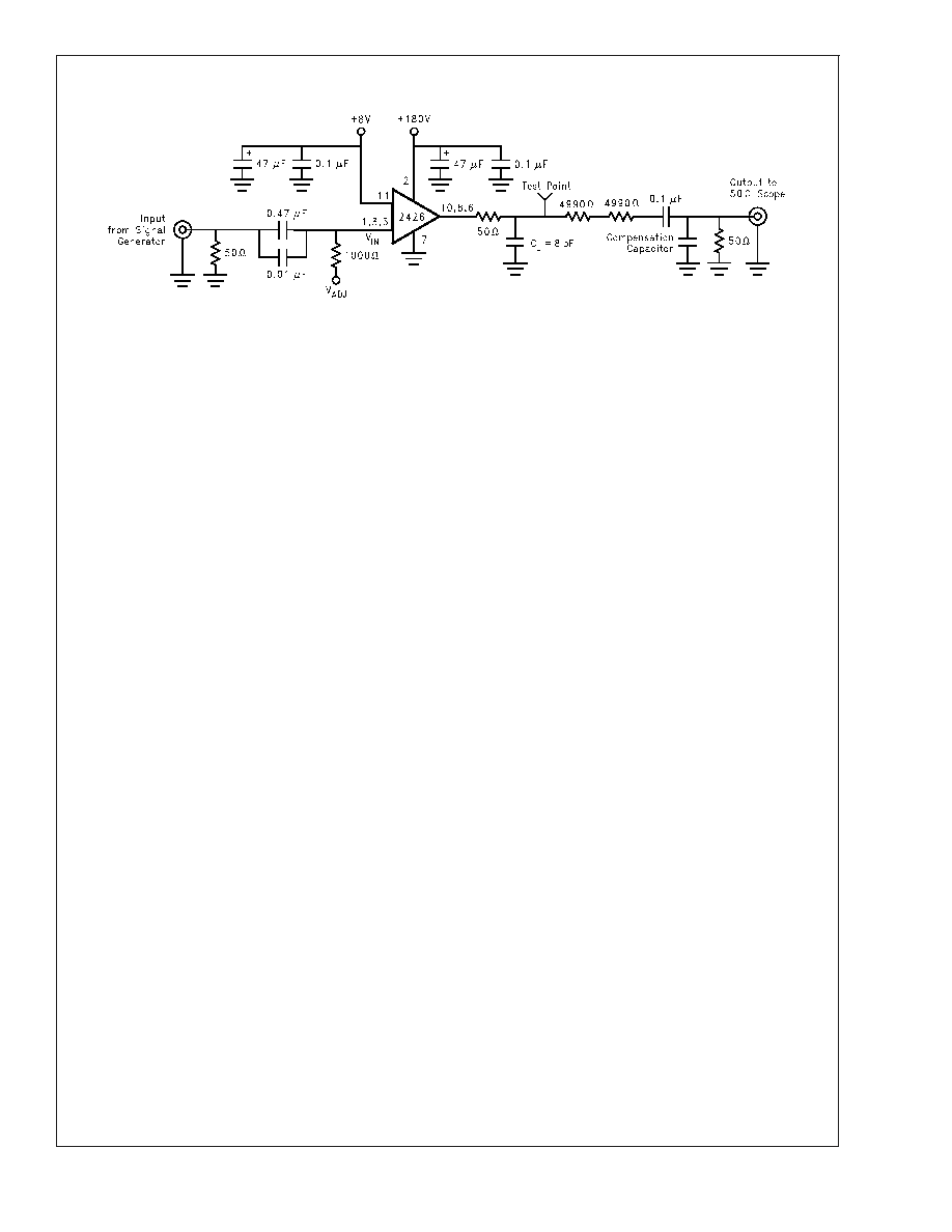
AC Test Circuit
Figure 3 shows a typical test circuit for evaluation of the LM2426TE. This circuit is designed to allow testing of the LM2426TE in
a 50
environment without the use of an expensive FET probe. The two 4990 resistors form a 400:1 divider with the 50
resistor and the oscilloscope. A test point is included for easy use of an oscilloscope probe.The compensation capacitor is used
to compensate the network to achieve flat frequency response.
20066403
Note: 8pF load includes parasitic capacitance.
FIGURE 3. Test Circuit (One Channel)
LM2426TE
www.national.com
3
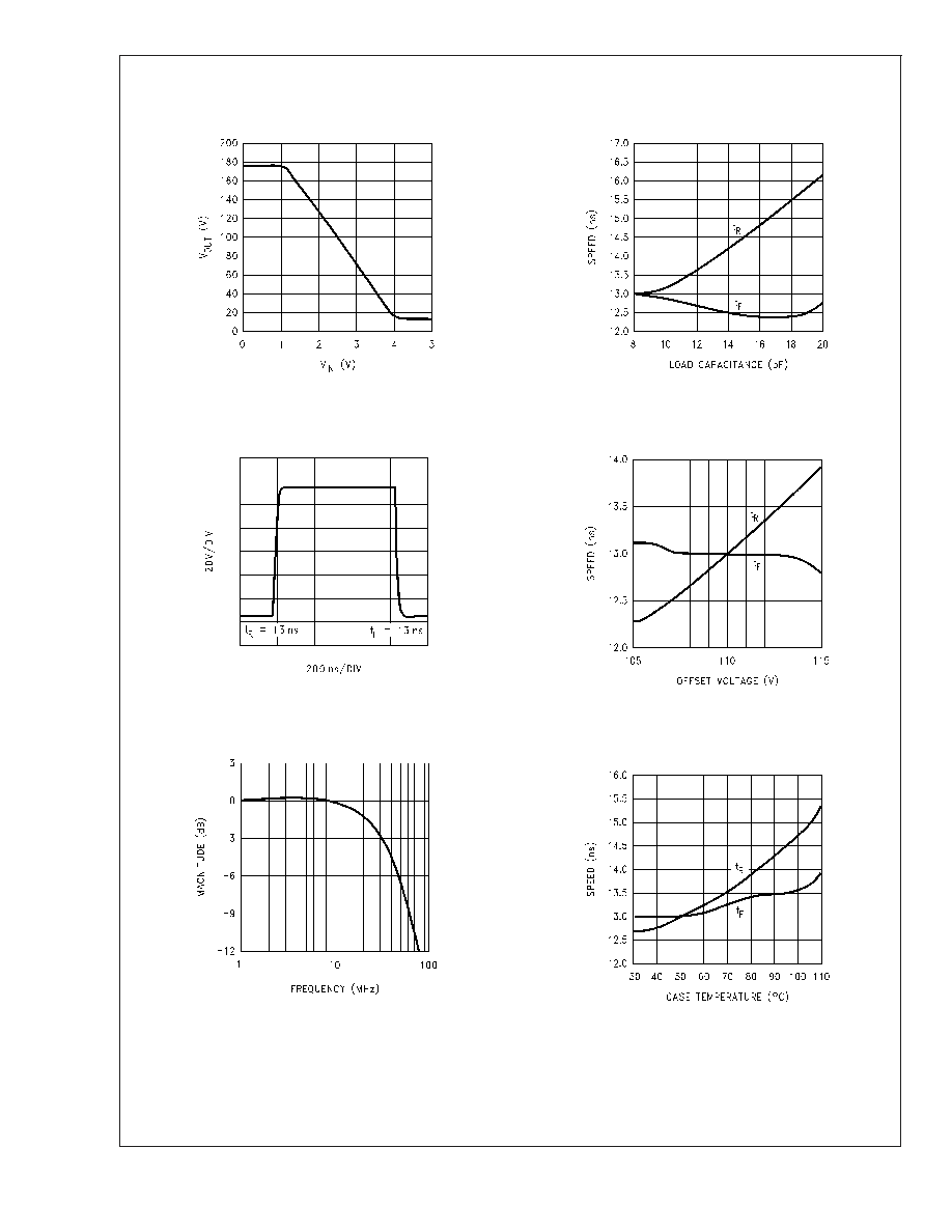
Typical Performance Characteristics
(V
CC
= +180V
DC
, V
BB
= +8V
DC
, C
L
= 8pF, V
OUT
= 110V
PP
(55V - 165V), Test Circuit - Figure 3 unless otherwise specified)
20066404
FIGURE 4. V
OUT
vs V
IN
20066406
FIGURE 5. LM2426TE Pulse Response
20066418
FIGURE 6. Bandwidth
20066405
FIGURE 7. Speed vs Load Capacitance
20066408
FIGURE 8. Speed vs Offset
20066409
FIGURE 9. Speed vs Case Temperature
LM2426TE
www.national.com
4

Typical Performance Characteristics
(V
CC
= +180V
DC
, V
BB
= +8V
DC
, C
L
= 8pF, V
OUT
= 110V
PP
(55V - 165V), Test Circuit - Figure 3 unless otherwise specified) (Continued)
20066407
FIGURE 10. Power Dissipation vs Frequency
20066416
FIGURE 11. Power Derating Curve
20066419
FIGURE 12. Cathode Pulse Response
LM2426TE
www.national.com
5