TL H 11967
LM2427
Triple
80
MHz
CRT
Driver
April 1995
LM2427
Triple 80 MHz CRT Driver
General Description
The LM2427 is a high performance triple CRT driver for
simplifying color monitor designs The device contains three
large signal transimpedance amplifiers and provides direct
cathode drive capability A plastic power package and pin-
to-pin compatibility make the LM2427 ideal for new designs
or as a low cost replacement for designs using the LH2426
or CR5527
Features
Y
Low-cost plastic power package
Y
Typical rise fall times of 3 5 ns
Y
80 MHz video bandwidth at 50 V
PP
with 8 pF load
Y
Operation from 80V power supply
Applications
Y
CRT driver for color monitors
Y
Drives CRT cathode directly
Y
Pin-to-pin compatible with the LH2426 and CR5527
CRT drivers
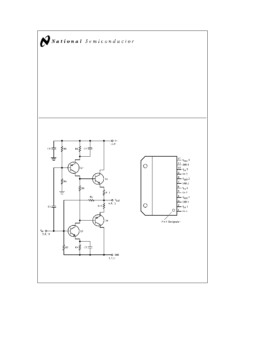
Schematic and Connection Diagrams
(One Section)
TL H 11967 � 1
TL H 11967 � 2
Top View
Order Number LM2427T
See NS Package Number MKT-TA12A
C1995 National Semiconductor Corporation
RRD-B30M115 Printed in U S A
Absolute Maximum Ratings
If Military Aerospace specified devices are required
please contact the National Semiconductor Sales
Office Distributors for availability and specifications
Supply Voltage V
a
a
85V
Safe Operating Power Consumption
14W
Storage Temperature Range T
STG
b
25 C to
a
100 C
Operating Temperature Range T
CASE
b
20 C to
a
90 C
Lead Temperature (Soldering 10 sec )
300 C
ESD Tolerance
TBD
Electrical Characteristics
V
a e
80V R
G
e
430X C1
e
47 pF C
L
e
8 pF 50 V
PP
output swing with 40V DC
offset See
Figure 1 T
CASE
e
25 C unless otherwise noted
Symbol
Parameter
Conditions
LM2427
Units
Min
Typical
Max
I
CC
Supply Current (per Amplifier)
No Input or Output Load
24
30
mA
V
INDC
Input Offset Voltage
1 4
1 6
1 8
V
V
OUTDC
Output Offset Voltage
34
40
46
V
t
R
Rise Time
10% to 90% (Note 1)
3 5
ns
t
F
Fall Time
90% to 10% (Note 1)
3 5
ns
A
V
Voltage Gain
b
11
b
13
b
14
V V
LE
Linearity Error
V
OUT
from
a
10V to
a
70V (Note 2)
5
%
D
A
V
Gain Matching
(Note 3)
0 2
dB
Note 1
Input signal t
r
t
f
k
1 5 ns f
in
e
1 MHz
Note 2
Linearity error is defined as The variation in small signal gain from
a
20V to
a
70V output with a 100 mVAC 1 MHz input signal
Note 3
Calculated value from voltage gain test on each channel
Typical Performance Characteristics
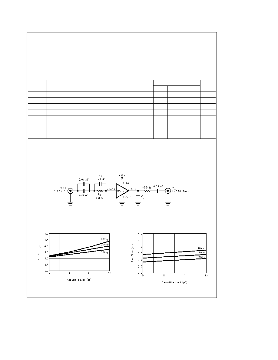
Typical Test Circuit (One Section)
TL H 11967 � 3
Note
C
L
total load capacltance includes all parasitic capacitances
FIGURE 1 Test Circuit (One Section)
This test circuit is used for both characteristic plots
Typical Rise Time vs Capacitive Loading
TL H 11967 � 10
Typical Fall Time vs Capacitive Loading
TL H 11967 � 5
2
Test Circuit
Figure 1 shows a typical test circuit for evaluation of the
LM2427 This circuit is designed to allow testing of the
LM2427 in a 50X environment such as a pulse generator
oscilloscope or network analyzer The 4950X resistor in se-
ries with the output of the LM2427 forms a 100 1 voltage
divider when connected to a 50X-input oscilloscope or net-
work analyzer To calibrate pulse generator set to 2 4 V
PP
into 50X
THEORY OF OPERATlON
The LM2427 is a triple channel transimpedance amplifier for
CRT's suitable for SVGA XGA IBM and Macintosh display
resolution monitors The LM2427 is pin-to-pin compatible
with the LH2426 and CR5527 CRT drivers The device is
packaged in the industry standard 12-lead SIP TO-220
molded plastic power package The heat sink is electrically
isolated and may be grounded for ease of manufacturing
and RFI EMI shielding
Applying an input current to the LM2427 will result in an
output voltage An input current of about
g
4 5 mA will pro-
vide a full output swing of
g
25V A resistor in series with the
input converts the device into a voltage amplifier with a
resistor value of 430X the voltage gain becomes
b
13
The LM2427 is a two stage amplifier configured in a push-
pull configuration (see schematic on front page) Q2 is bi-
ased by resistors R4 and R5 Q1 gets its bias through a
5700X feedback resistor and the input biasing current The
bases of Q1 and Q2 are capacitively coupled and therefore
Q2 will be actively driven
The emitter resistors of Q1 and Q2 are bypassed with small
capacitors This increases the gain of the stage for high
frequencies and increases the bandwidth of the amplifier
Emitter followers Q3 and Q4 isolate the input stage from the
output capacitance load and minimizes the circuit sensitivity
to load capacitance
The power supply pin is intemally bypassed If low frequen-
cies are present in the power supply line an electrolytic
capacitor is recommended
Application Hints
The LM2427 is designed as a triple power amplifier for deliv-
ering red green and blue video signals to a cathode ray
tube (CRT) It can provide a 50V output swing and energize
a 12 ns pixel at a CRT cathode with 8 pF of capacitance
As with any CRT driver when designing a video amplifier
board with the LM2427 careful attention should be paid at
reducing stray capacitance along the entire video signal
path This is especially important in the path between the
output of the CRT driver and the cathodes because any
additional capacitance load will increase rise and fall times
and will result in reduced picture quality
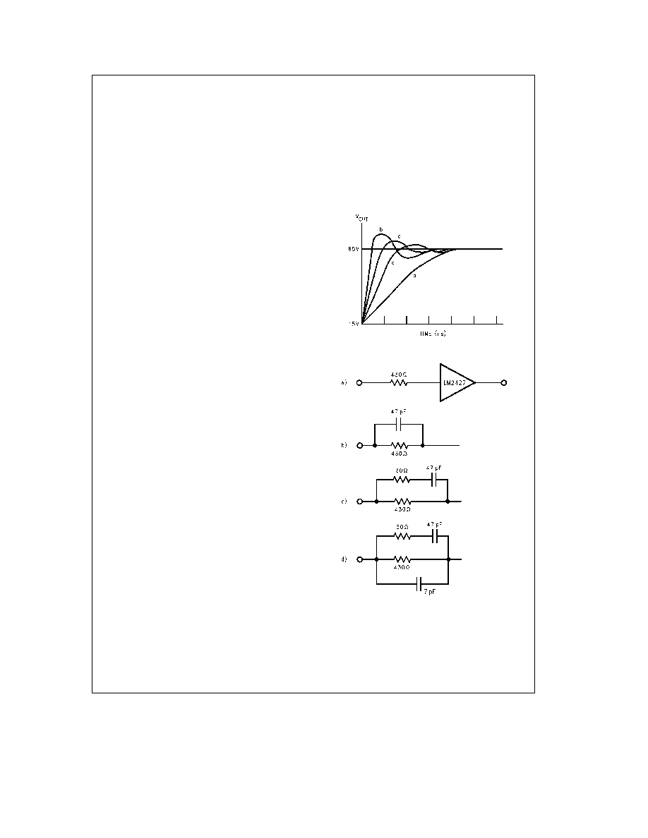
INPUT NETWORKS
The voltage gain and the response of the amplifiers can be
set by adding an R-C network to the input
A 430X resistor in series with the input will set the voltage
gain to
b
13 but this will increase the rise and fall times of
the system (see
Figure 2a )
Bypassing the resistor with a capacitor of about 47 pF will
restore the rise and fall times but will result in some over-
shoot
(Figure 2b)
Adding a resistor in series with the 47 pF capacitor will re-
duce the overshoot but also increases the rise and fall
times
(Figure 2c)
The addition of a second capacitor offers a compromise
between the above networks by improving the rise and fall
times at the expense of some overshoot
(Figure 2d)
Suggested values for the resistors and capacitors are
shown however optimum values may differ depending
upon the stray inductances and capacitances present in dif-
ferent board layouts
TL H 11967 � 6
FIGURE 2 Influence of Input Networks
on Switching Performance
3

Application Hints
(Continued)
TILT AND OVERSHOOT COMPENSATlON
When a low frequency square is displayed on a monitor
screen some tilt may appear on the video signal due to the
large power and thermal dissipation changes in the input
transistors This problem is illustrated in
Figure 3
TL H 11967 � 7
FIGURE 3 Tilt on a Low Frequency
Signal and Its Effects
The tilt can be compensated by adding an external RC feed-
back network as shown in
Figure 4 The RC feedback helps
by reducing the gain of the amplifier during the edge tran-
sition for a duration corresponding to
u
The values of R and
C should be selected so that the gain is reduced (DV
e
0)
for the duration of the tilt (
u
)
TL H 11967 � 8
FIGURE 4 RC Feedback Network for Tilt Compensation
To find the value of resistor R the following formula can be
used
R
e
(100
b
x%)
x%
R
F
where x% is the percentage value of DV to the peak-to-
peak output swing (V
PP
) R
F
is internally fixed to 5700X
The value of capacitor C is determined by
C
e
u
R
where
u
is the duration of the tilt
For optimum results in a specific application the values for
R and C may need to be tested and adjusted in the given
application board
PROTECTlNG AMPLIFIER OUTPUT
FROM TUBE ARCING
During normal CRT operation internal arcing may occasion-
ally occur Spark gap protectors will limit the maximum volt-
age but to a value that is much higher than allowable on the
LM2427 This fast high voltage high energy pulse can dam-
age the LM2427 output stage The addition of two current
limiting resistors of 50X to 100X total and clamping diodes
D1 and D2 will provide protection but will slow down the
response The diodes should have a fast transient re-
sponse high peak current rating low series impedance and
low shunt capacitance FDH400 or equivalent diodes are
recommended Adding a series peaking inductor of 100 nH
to 150 nH will restore the bandwidth and provide additional
protection (See
Figure 5 )
The value of the inductor can be calculated from
Lp
e
(R
O
a
R
1
a
R
2
)
2
2 4
C
L
where C
L
is the total load and R
O
is the intrinsic high fre-
quency output resistance of the amplifier generally 160X
TL H 11967 � 9
FIGURE 5 One Section of the LM2427
with Tilt Compensation Arc Protection
and Peaking Inductance L
P
in the Output
SHORT CIRCUIT PROTECTION
WARNING
To provide maximum output speed the LM2427 does not
have short circuit protection Shorting the output can de-
stroy the device
SUPPLY BYPASSlNG
Although the LM2427 has internal supply bypassing some
values of supply line inductance can cause ringing in the
supply lines If this occurs an additional bypass capacitor or
a low-pass filter should be placed as close as possible to
the supply (V
a
) pins of the LM2427
CAPACITlVE LOADS
The LM2427 is designed to drive capacitive loads however
the very high output slew rate of about 13 700 V ms can
result in charging currents of over 200 mA into a 20 pF load
These very high currents can damage the output transistors
HEAT SlNKlNG
Power consumption by the LM2427 will depend on the sup-
ply voltage used the output loading the peak-to-peak out-
put swing and the operating frequency Since the LM2427
will dissipate up to 14W an external heatsink is always re-
quired The maximum allowed case temperature is 90 C To
calculate maximum heatsink thermal resistance use the fol-
lowing formula
R
th
e
(90 C
b
Max Ambient)
14
4

PC BOARD LAYOUT CONSIDERATIONS
Input pins 2 6 and 10 are amplifier summing junctions All
connections to these points should be as short as possible
and should be separated from other signals The compo-
nents connected to these pins should be located close to
the LM2427 and the total conductor length connected to
these points should be no more than one inch
For optimum performance an adequate ground plane isola-
tion between channels good supply bypassing and minimiz-
ing unwanted feedback are necessary Also the length of
the signal traces from the preamplifier to the LM2427 and
from the LM2427 to the CRT cathode should be as short as
possible The following references are recommended
Ott Henry W
``Noise Reduction Techniques in Electronic
Systems'' John Wiley
Sons New York 1976
``Guide to CRT Video Design'' National Semiconductor Ap-
plication Note 861
5