LM2457
Monolithic Triple 7.5nS CRT Driver With Integrated
Clamp and G1 Blanking
General Description
The LM2457 driver is an integrated high voltage triple CRT
driver circuit designed for use in color monitor applications.
The input signal interface to the IC is a multiplexed signal
containing both clamp and video signal information, relative
to an external 1.7 VDC reference.
The IC contains three high gain, differential input, high input
impedance, wide band amplifiers which directly drive the
RGB cathodes of a CRT. Each channel has its gain internally
set to -52 and can drive CRT capacitive loads as well as
resistive loads present in other applications, limited only by
the package's power dissipation.
Integrated with the driver is a triple video clamp circuit for DC
recovery of each of the AC coupled video outputs. The DC
clamp circuit amplifies the clamp signal that is multiplexed on
the video signal input. The DC clamp amplifiers are high
gain, differential input, high input impedance amplifiers, set-
ting a low impedance DC level at the clamp output which can
be used to restore the DC level of the cathode drive. Each
channel has a gain that is internally set to +75.
Also integrated within the package is a 43V
p-p
vertical blank-
ing driver that is designed to drive the vertical retrace blank-
ing signal to the G1. This is a current limited, low impedance
output capable of driving normal G1 decoupling capaci-
tances via an external resistor.
The output of the G1 driver can also be used to drive a
voltage boost capacitor (22uF). When connected between
the G1 drive output and the 120v supply input pin, a 120v
boost supply is achieved which can be used to drive the
internal DC clamp circuit, thereby eliminating the require-
ment for a 120V clamp supply.
The IC is packaged in an industry standard 15 lead TO-220
molded plastic power package.
Features
n
7.5ns low power driver
n
Three integrated active clamp circuits
n
Integrated 120V supply and G1 vertical blank drive
circuit
n
Multiplexed signal interface to LM125X OSD Pre-amp
minimizes pin count while increasing functionality
n
External System voltage reference
n
Convenient TO-220 staggered lead package
Recommended Applications
n
1024 x 768 Resolution displays up to 85Hz refresh
n
Pixel clock frequencies up to 95MHz
n
Monitor requiring horizontal video blanking
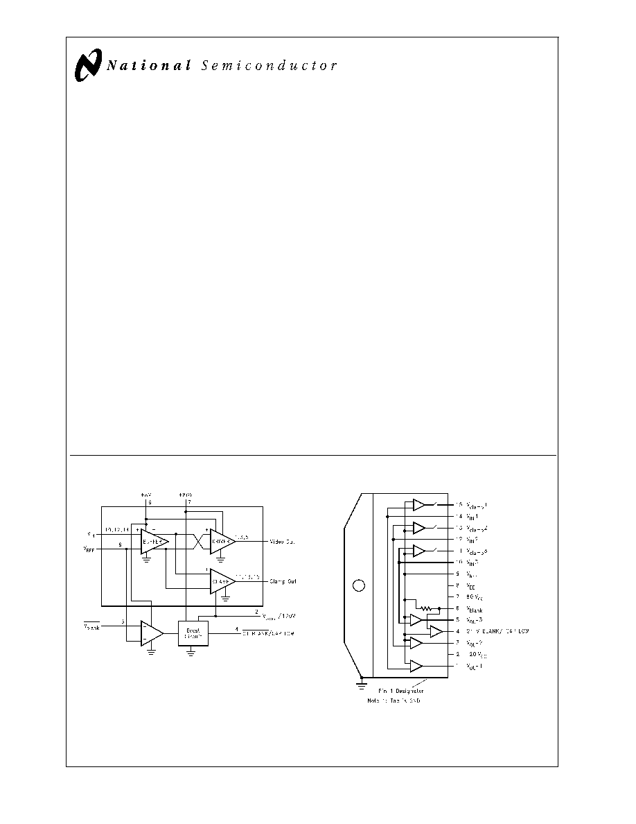
Block Diagram
Package Pinout
DS101379-1
FIGURE 1. LM2457 Block Diagram
DS101379-2
FIGURE 2. LM2457 Package Pinout
Order Number LM2457TA
October 2000
LM2457
Monolithic
T
riple
7.5nS
CRT
Driver
W
ith
Integrated
Clamp
and
G1
Blanking
� 2000 National Semiconductor Corporation
DS101379
www.national.com
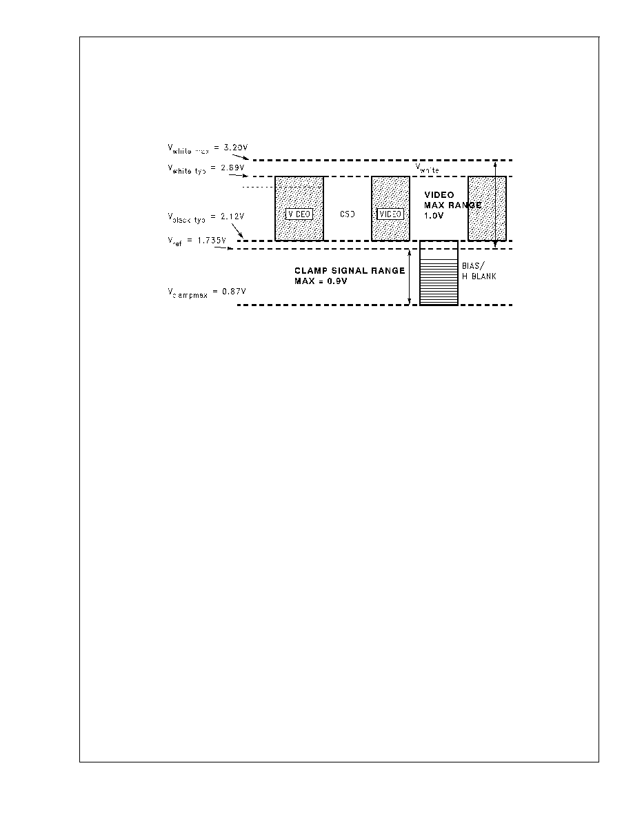
Special Features
MULTIPLEXED VIDEO SIGNAL INPUT
The LM2457 accepts the multiplexed video signal from the
LM1253 which contains the video signal and DC clamp level.
This multiplexed signal is shown in
Figure 3. It was designed
to simplify the interface between the pre-amp and CRT
Driver. Slightly over 1V of dynamic range is provided for the
video and OSD portions of the waveform. The clamp signal
control voltage range is approximately 0.9V. The typical
numbers for the black and white levels shown correspond to
a nominal swing of 40V
P-P
at the video outputs of the
LM2457.
DS101379-3
FIGURE 3. National LM1253 Multiplexed Video Signal
LM2457
www.national.com
2
Absolute Maximum Ratings
(Notes 1, 3)
If Military/Aerospace specified devices are required,
please contact the National Semiconductor Sales Office/
Distributors for availability and specifications.
80V Voltage, V
CC1
+90V
120V Supply V
CC2
+130V
Bias Voltage, V
BB
+15V
Input Voltage, V
IN
0V to 4V
V
BLANK
Input Voltage, V
BLANK
0V to V
BB
V
Storage Temperature Range, T
STG
-65�C to +150�C
Lead Temperature
(Soldering,
<
10 sec.)
300�C
ESD Tolerance, Human Body
Model
2 kV
ESD Tolerance, Machine Model
200V
Limits of Operating Ranges
(Note 2)
V
CC1
+60V to +85V
V
BOOST
V
CC1
to +125V
V
BB
7.0V to +9V
V
IN
0.8V to +3.5V
V
REF
+1.6V to +1.9V
V
BLANK
Input Voltage, V
BLANK
0V to 5.5V
V
OUT
+15V to +75V
V
CLAMP
+55V to +118V
Case Temperature
-20�C to 100�C
AC Driver Electrical Characteristics
(See
Figure 4 for Test Circuit)
Unless otherwise noted: V
CC
= +80V
DC
, V
BB
= +8V
DC
, V
IN
= 2.50V
DC
, C
L
= 8pF, Output = 40V
PP
(25-65) at 1MHz, T
C
= 50�C,
V
REF
= 1.735V
DC
, HEATSINK MUST BE GROUNDED.
Symbol
Parameter
Conditions
Min
Typ
Max
Units
I
CC1MAX
V
CC
Supply Current
All 3 Channels, No Output Load
32
mA
I
BBMAX
Maximum Bias Current
All 3 Channels
15
mA
V
OUTTYP
Typical DC Output Voltage
V
IN
= 2.100 V
DC
61
65
69
V
DC
A
VTYP
Typical DC Voltage Gain
No AC Input Signal
-52
T
RTYP
Typical Rise Time
10% to 90%, (Note 5)
7.5
ns
+OS
Overshoot on Rising Edge
5
%
t
FTYP
Typical Fall Time
90% to 10%, (Note 5)
7.5
ns
-OS
Overshoot on Falling Edge
1
%
LE
TYP
Typical Linearity Error
V
IN
2.0 V
DC
to 3.0 V
DC
, (Note 4)
6
%
Note 1: Limits of "Absolute Maximum Ratings" indicate limits below which damage to the device will not occur.
Note 2: Limits of "Operating Ratings" indicate required boundaries of conditions for which the device is functional, but is not guaranteed to meet specific performance
limits.
Note 3: All voltages are measured with respect to GND, unless otherwise specified.
Note 4: Linearity error is the variation in DC gain from V
IN
= 2.0V to 3.0V.
Note 5: Input from signal generator: t
r
, t
f
<
1ns.
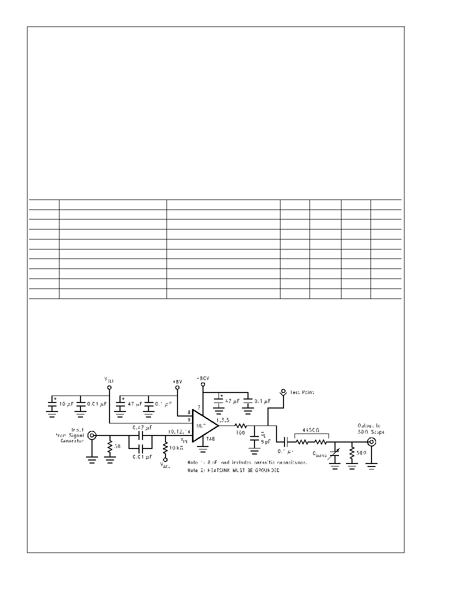
Driver Test Circuit
Figure 4 shows the test circuit for the LM2457. This circuit allows testing of the LM2457 in a 50
environment as well as with a
FET probe. The 4950
resistor at the output forms a 200:1 voltage divider when connected to a 50
load. C
COMP
is used to
flatten the frequency response of the 200:1 divider. Performance will be affected slightly by the 5K load.
DS101379-4
FIGURE 4. Test Circuit (One Channel)
LM2457
www.national.com
3
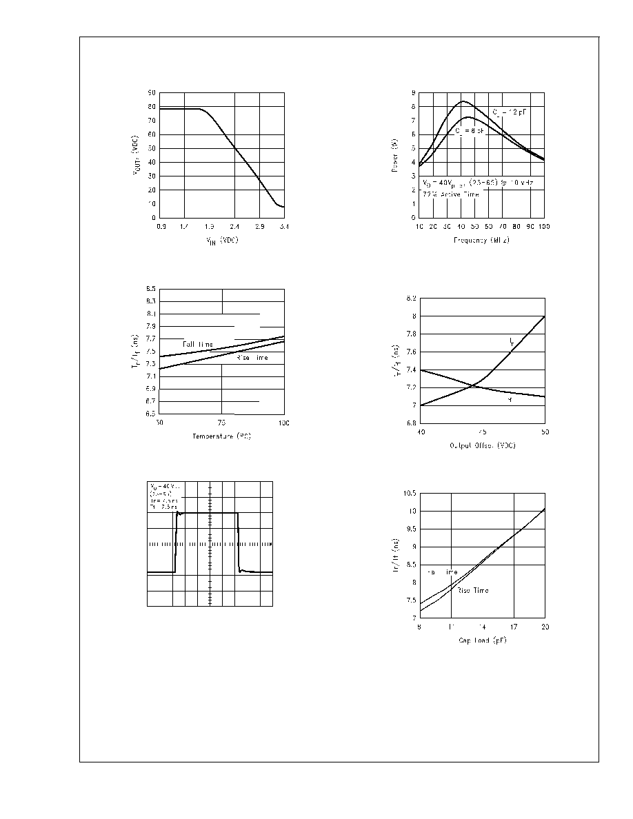
Typical Performance Characteristics
(Unless otherwise noted: V
CC
= 80V
DC
, V
BB
= 8V
DC
, C
L
= 8pF, T
C
= 50�C.
DS101379-22
FIGURE 5. CRT Driver V
O
vs V
IN
DS101379-23
FIGURE 6. CRT Driver Speed vs. Temperature
DS101379-26
FIGURE 7. CRT Driver Transient Response
DS101379-8
FIGURE 8. CRT Driver Power
Dissipation vs. Frequency
DS101379-24
FIGURE 9. CRT Driver Speed vs. Offset
DS101379-25
FIGURE 10. Speed vs. Load
LM2457
www.national.com
4
DC CLAMP Electrical Characteristic Targets and Limits
(See
Figure 11 for Test Circuit)
Unless otherwise noted: V
CC1
= +80V, V
CC2
= 120V, V
BB
= +8V, V
IN
= 1.4V
DC
, T
C
= 50�C, V
REF
= 1.735V, SW1 open.
HEATSINK MUST BE GROUNDED.
Symbol
Parameter
Conditions
Min
Typ
Max
Units
I
CC2
V
CC2
Supply Current
All Channel, No AC input signal,
V
IN
= 1.25V
2.4
mA
V
OUT
Typical DC Output Voltage
No AC Input Signal, V
IN
= 1.4V
95
V
DC
A
VTYP
Typical DC Voltage Gain
No AC Input Signal
75
LE
TYP
Typical Linearity Error
No AC Input Signal (Note 6)
2
%
Note 6: Linearity Error is the variation in DC gain from V
IN
= 1.0V to V
IN
= 1.5V.
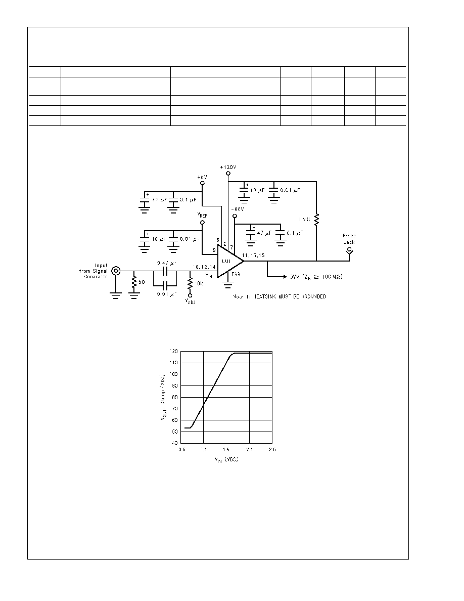
Clamp Amplifier Test Circuit
Figure 11 shows the test circuit for evaluation of the LM2457 clamp amplifier. A high impedance VM (
>
100 M
) is used for DC
measurements at the outputs.
DS101379-11
FIGURE 11. Test Circuit (One Channel)
DS101379-12
FIGURE 12. Clamp Circuit V
O
vs. V
IN
LM2457
www.national.com
5