 | –≠–ª–µ–∫—Ç—Ä–æ–Ω–Ω—ã–π –∫–æ–º–ø–æ–Ω–µ–Ω—Ç: LM2462 | –°–∫–∞—á–∞—Ç—å:  PDF PDF  ZIP ZIP |

LM2462
Monolithic Triple 3 ns CRT Driver
General Description
The LM2462 is an integrated high voltage CRT driver circuit
designed for use in color monitor applications. The IC con-
tains three high input impedance, wide band amplifiers
which directly drive the RGB cathodes of a CRT. Each
channel has its gain internally set to -20 and can drive CRT
capacitive loads as well as resistive loads present in other
applications, limited only by the package's power dissipation.
The IC is packaged in an industry standard 11-lead TO-220
molded plastic power package. See Thermal Considerations
section.
Features
n
Higher gain to match LM126X CMOS preamplifiers
n
0V to 3.75V input range
n
Stable with 0≠20 pF capacitive loads and inductive
peaking networks
n
Convenient TO-220 staggered lead package style
n
Maintains standard LM240X Family pinout which is
designed for easy PCB layout
Applications
n
1600 x 1200 displays up to 85Hz refresh
n
Pixel clock frequencies up to 230 MHz
n
Monitors using video blanking
Schematic and Connection Diagrams
DS200376-1
FIGURE 1. Simplified Schematic Diagram
(One Channel)
DS200376-2
Note: Tab is at GND
Top View
Order Number LM2462TA
NS Package Number: TA11B
February 2002
LM2462
Monolithic
T
riple
3
n
s
CRT
Driver
© 2002 National Semiconductor Corporation
DS200376
www.national.com
Absolute Maximum Ratings
(Notes 1, 3)
If Military/Aerospace specified devices are required,
please contact the National Semiconductor Sales Office/
Distributors for availability and specifications.
Supply Voltage (V
CC
)
+90V
Bias Voltage (V
BB
)
+16V
Input Voltage (V
IN
)
0V to 4.5V
Storage Temperature Range (T
STG
)
-65∞C to +150∞C
Lead Temperature
(Soldering,
<
10 sec.)
300∞C
ESD Tolerance, Human Body Model
2kV
Machine Model
250V
Operating Ranges
(Note 2)
V
CC
+60V to +85V
V
BB
+8V to +15V
V
IN
+0V to +3.75V
V
OUT
+15V to +75V
Case Temperature
-20∞C to +100∞C
Do not operate the part without a heat sink.
Electrical Characteristics
(See
Figure 2 for Test Circuit)
Unless otherwise noted: V
CC
= +80V, V
BB
= +12V, C
L
= 8 pF, T
C
= 50∞C
DC Tests: V
IN
= 2.25VDC
AC Tests: Output = 40V
PP
(25V - 65V) at 1MHz
Symbol
Parameter
Conditions
LM2462
Units
Min
Typical
Max
I
CC
Supply Current
All Three Channels, No Input Signal,
No Output Load
63
mA
I
BB
Bias Current
All Three Channels
42
mA
V
OUT
DC Output Voltage
No AC Input Signal, V
IN
= 1.25V
62
65
68
V
DC
A
V
DC Voltage Gain
No AC Input Signal
-18
-20
-22
A
V
Gain Matching
(Note 4), No AC Input Signal
1.0
dB
LE
Linearity Error
(Notes 4, 5), No AC Input Signal
8
%
t
R
Rise Time
(Note 6), 10% to 90%
3.0
3.8
ns
t
F
Fall Time
(Note 6), 90% to 10%
3.3
4.1
ns
OS
Overshoot
(Note 6)
8
%
Note 1: Absolute Maximum Ratings indicate limits beyond which damage to the device may occur.
Note 2: Operating ratings indicate conditions for which the device is functional, but do not guarantee specific performance limits. For guaranteed specifications and
test conditions, see the Electrical Characteristics. Datasheet min/max specification limits are guaranteed by design, test, or statistical analysis. The guaranteed
specifications apply only for the test conditions listed. Some performance characteristics may change when the device is not operated under the listed test
conditions.
Note 3: All voltages are measured with respect to GND, unless otherwise specified.
Note 4: Calculated value from Voltage Gain test on each channel.
Note 5: Linearity Error is the variation in dc gain from V
IN
= 1.0V to V
IN
= 3.5V.
Note 6: Input from signal generator: t
r
, t
f
<
1 ns.
Note 7: Datasheet min/max specification limits are guaranteed by design, test, or statistical analysis.
LM2462
www.national.com
2
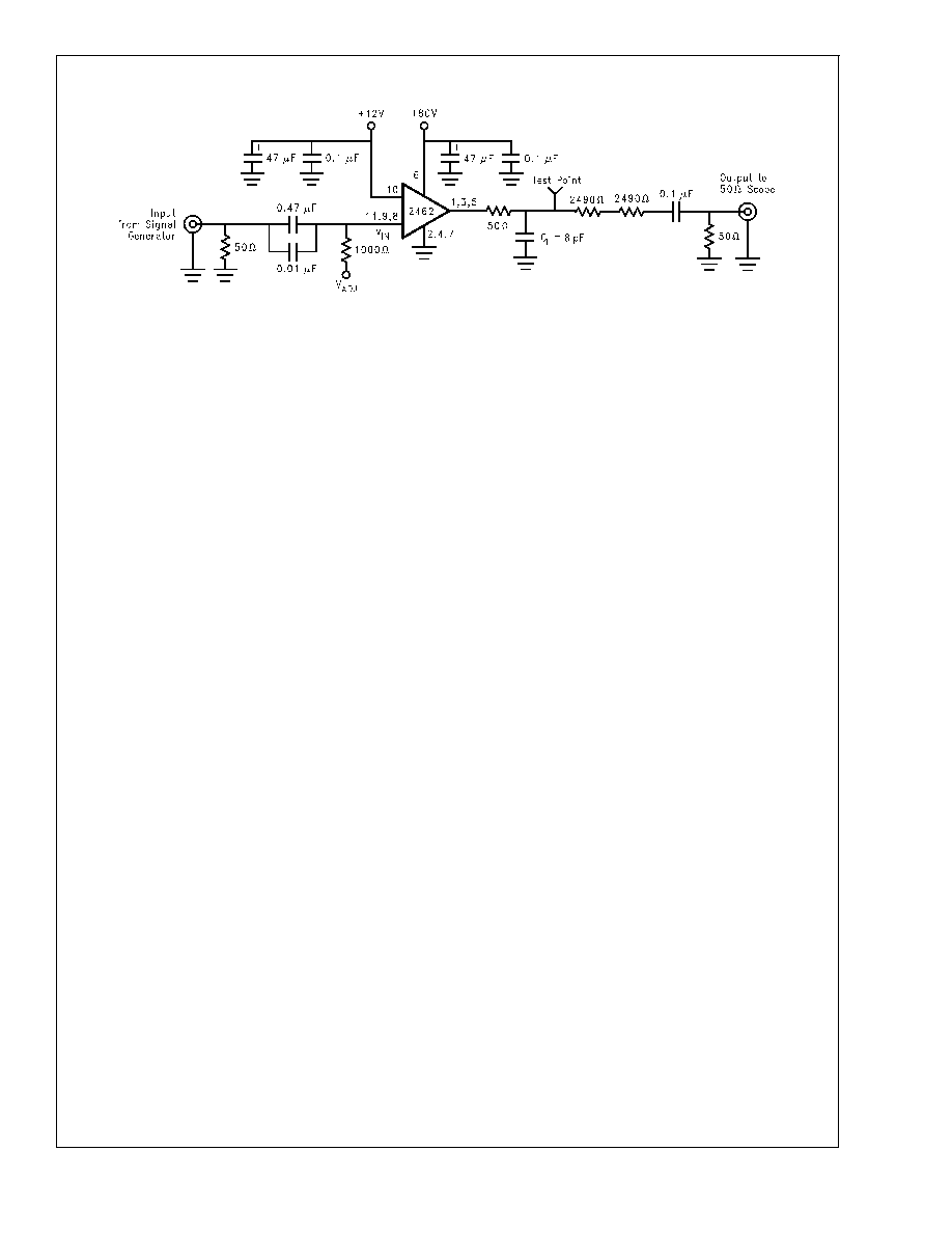
AC Test Circuit
Figure 2 shows a typical test circuit for evaluation of the LM2462. This circuit is designed to allow testing of the LM2462 in a 50
environment without the use of an expensive FET probe. The two 2490
resistors form a 200:1 divider with the 50
resistor and
the oscilloscope. A test point is included for easy use of an oscilloscope probe.
DS200376-3
Note: 8 pF load includes parasitic capacitance.
FIGURE 2. Test Circuit (One Channel)
LM2462
www.national.com
3
Typical Performance Characteristics
(V
CC
= +80V
DC
, V
BB
= +12V
DC
, C
L
= 8pF, V
OUT
= 40V
PP
(25V-65V), T
CASE
= 60∞C, Test Circuit -
Figure 2 unless otherwise specified)
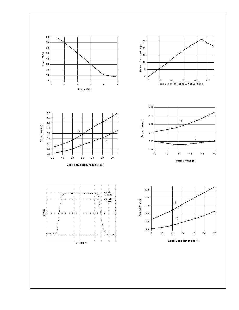
DS200376-19
FIGURE 3. V
OUT
vs V
IN
DS200376-17
FIGURE 4. Speed vs Temp.
DS200376-25
FIGURE 5. LM2462 Pulse Response
T
CASE
= 50∞C
DS200376-24
FIGURE 6. Power Dissipation vs Frequency
DS200376-18
FIGURE 7. Speed vs Offset
DS200376-16
FIGURE 8. Speed vs Load Capacitance
LM2462
www.national.com
4

Theory of Operation
The LM2462 is a high voltage monolithic three channel CRT
driver suitable for high resolution display applications. The
LM2462 operates with 80V and 12V power supplies. The
part is housed in the industry standard 11-lead TO-220
molded plastic power package.
The circuit diagram of the LM2462 is shown in
Figure 1. The
PNP emitter follower, Q5, provides input buffering. Q1 and
Q2 form a fixed gain cascode amplifier with resistors R1 and
R2 setting the gain at -20. Emitter followers Q3 and Q4
isolate the high output impedance of the cascode stage from
the capacitance of the CRT cathode which decreases the
sensitivity of the device to changes in load capacitance. Q6
provides biasing to the output emitter follower stage to re-
duce crossover distortion at low signal levels.
Figure 2 shows a typical test circuit for evaluation of the
LM2462. This circuit is designed to allow testing of the
LM2462 in a 50
environment without the use of an expen-
sive FET probe. In this test circuit, the two 2.49k
resistors
form a 200:1 wideband, low capacitance probe when con-
nected to a 50
coaxial cable and a 50
load (such as a
50
oscilloscope input). The input signal from the generator
is ac coupled to the base of Q5.
Application Hints
INTRODUCTION
National Semiconductor (NSC) is committed to provide ap-
plication information that assists our customers in obtaining
the best performance possible from our products. The fol-
lowing information is provided in order to support this com-
mitment. The reader should be aware that the optimization of
performance was done using a specific printed circuit board
designed at NSC. Variations in performance can be realized
due to physical changes in the printed circuit board and the
application. Therefore, the designer should know that com-
ponent value changes may be required in order to optimize
performance in a given application. The values shown in this
document can be used as a starting point for evaluation
purposes. When working with high bandwidth circuits, good
layout practices are also critical to achieving maximum per-
formance.
IMPORTANT INFORMATION
The LM2462 performance is targeted for the high end 19"
and 21" market with resolutions up to 1600 x 1200 and an
85Hz refresh rate. The application circuits shown in this
document were specifically designed to optimize the perfor-
mance of the LM2462 as well as protect it from damage due
to a CRT arc-over. If another member of the LM246X family
is used, please refer to its datasheet.
POWER SUPPLY BYPASS
Since the LM2462 is a wide bandwidth amplifier, proper
power supply bypassing is critical for optimum performance.
Improper power supply bypassing can result in large over-
shoot, ringing or oscillation. 0.1 µF capacitors should be
connected from the supply pins, V
CC
and V
BB
, to ground, as
close to the LM2462 as is practical. Additionally, a 47 µF or
larger electrolytic capacitor should be connected from both
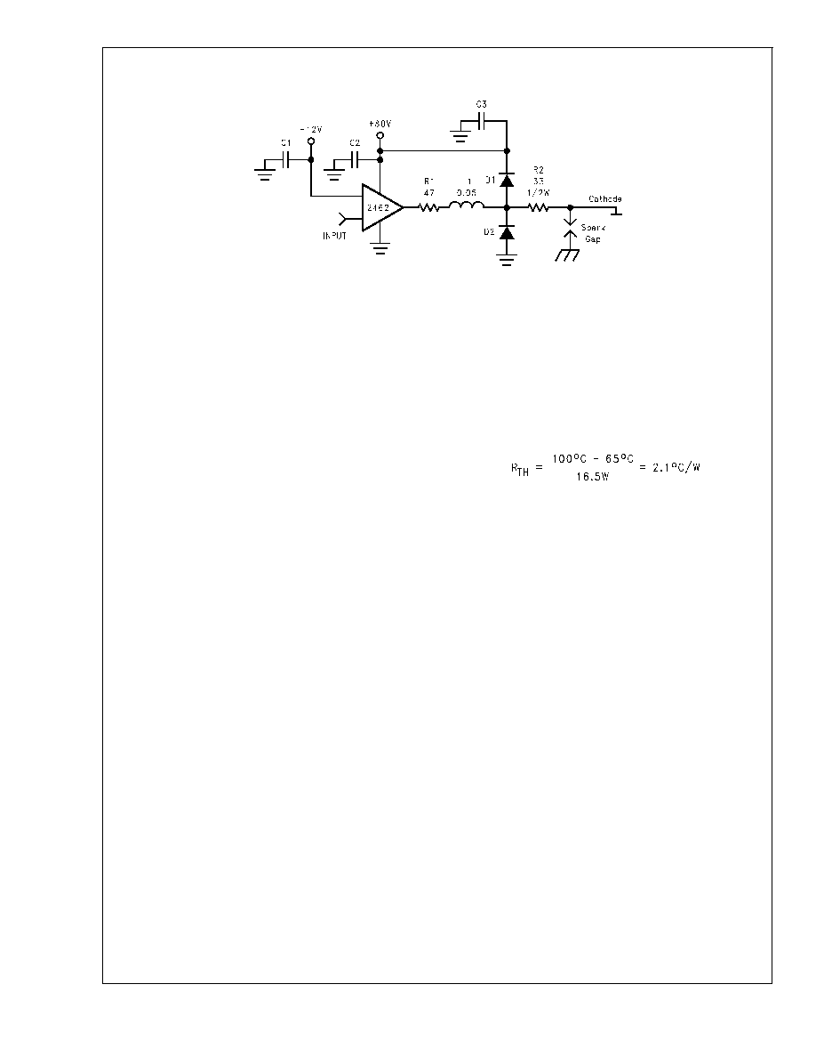
supply pins to ground reasonably close to the LM2462.
ARC PROTECTION
During normal CRT operation, internal arcing may occasion-
ally occur. Spark gaps, in the range of 200V, connected from
the CRT cathodes to CRT ground will limit the maximum
voltage, but to a value that is much higher than allowable on
the LM2462. This fast, high voltage, high energy pulse can
damage the LM2462 output stage. The application circuit
shown in
Figure 9 is designed to help clamp the voltage at
the output of the LM2462 to a safe level. The clamp diodes,
D1 and D2, should have a fast transient response, high peak
current rating, low series impedance and low shunt capaci-
tance. FDH400 or equivalent diodes are recommended. Do
not use 1N4148 diodes for the clamp diodes. D1 and D2
should have short, low impedance connections to V
CC
and
ground respectively. The cathode of D1 should be located
very close to a separately decoupled bypass capacitor (C3 in
Figure 9). The ground connection of D2 and the decoupling
capacitor should be very close to the LM2462 ground. This
will significantly reduce the high frequency voltage transients
that the LM2462 would be subjected to during an arcover
condition. Resistor R2 limits the arcover current that is seen
by the diodes while R1 limits the current into the LM2462 as
well as the voltage stress at the outputs of the device. R2
should be a
1
/
2
W solid carbon type resistor. R1 can be a
1
/
4
W
metal or carbon film type resistor. Having large value resis-
tors for R1 and R2 would be desirable, but this has the effect
of increasing rise and fall times. Inductor L1 is critical to
reduce the initial high frequency voltage levels that the
LM2462 would be subjected to. The inductor will not only
help protect the device but it will also help optimize rise and
fall times as well as minimize EMI. For proper arc protection,
it is important to not omit any of the arc protection compo-
nents shown in
Figure 9.
LM2462
www.national.com
5
Application Hints
(Continued)
OPTIMIZING TRANSIENT RESPONSE
Referring to
Figure 9, there are three components (R1, R2
and L1) that can be adjusted to optimize the transient re-
sponse of the application circuit. Increasing the values of R1
and R2 will slow the circuit down while decreasing over-
shoot. Increasing the value of L1 will speed up the circuit as
well as increase overshoot. It is very important to use induc-
tors with very high self-resonant frequencies, preferably
above 300 MHz. Ferrite core inductors from J.W. Miller
Magnetics (part # 78-FRK) were used for optimizing the
performance of the device in the NSC application board. The
values shown in
Figure 9 can be used as a good starting
point for the evaluation of the LM2462. Using a variable
resistor for R1 will simplify finding the value needed for
optimum performance in a given application. Once the opti-
mum value is determined, the variable resistor can be re-
placed with a fixed value.
EFFECT OF LOAD CAPACITANCE
Figure 8 shows the effect of increased load capacitance on
the speed of the device. This demonstrates the importance
of knowing the load capacitance in the application. The rise
time increased about 0.08 nsec for an increase of 1 pF in the
load capacitance. The fall time increased about 0.14 nsec for
a 1 pF increase in the load capacitance.
EFFECT OF OFFSET
Figure 7 shows the variation in rise and fall times when the
output offset of the device is varied from 40 to 50 V
DC
. The
rise time varies less than 0.10 nsec. The fall time varies a
little under 0.50 nsec, but only 0.15 nsec from the fastest fall
time at 40V offset.
THERMAL CONSIDERATIONS
Figure 4 shows the performance of the LM2462 in the test
circuit shown in
Figure 2 as a function of case temperature.
The figure shows that both the rise and fall times of the
LM2462 increase by approximately 46% as the case tem-
perature increases from 30∞C to 95∞C. This corresponds to a
speed degradation of 7.1% for every 10∞C rise in case
temperature.
Figure 6 shows the maximum power dissipation of the
LM2462 vs. Frequency when all three channels of the device
are driving an 8pF load with a 40V
p-p
alternating one pixel
on, one pixel off. The graph assumes a 72% active time
(device operating at the specified frequency) which is typical
in a monitor application. The other 28% of the time the
device is assumed to be sitting at the black level (65V in this
case). This graph gives the designer the information needed
to determine the heat sink requirement for his application.
The designer should note that if the load capacitance is
increased the AC component of the total power dissipation
will also increase.
The LM2462 case temperature must be maintained below
100∞C. If the maximum expected ambient temperature is
65∞C and the maximum power dissipation is 16.5W (from
Figure 6, 100MHz bandwidth) then a maximum heat sink
thermal resistance can be calculated:
This example assumes a capacitive load of 8 pF and no
resistive load.
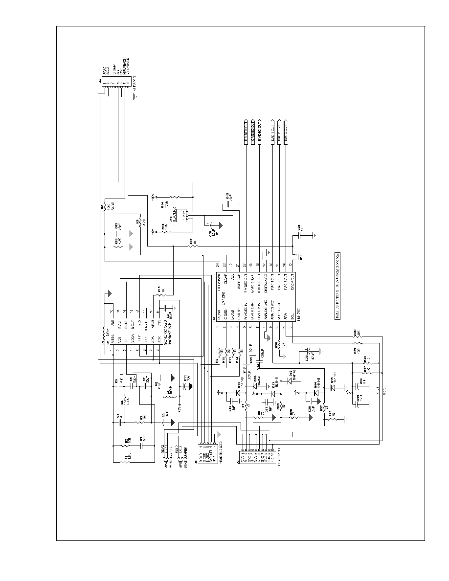
TYPICAL APPLICATION
A typical application of the LM2462 is shown in
Figure 10
and
Figure 11. Used in conjunction with an LM1262 video
pre-amp and an LM2479/2480 bias clamp, a complete video
channel from monitor input to CRT cathode can be achieved.
Performance is ideal for 1600 X 1200 resolution displays
with pixel clock frequencies up to 230MHz.
Figure 10 and
Figure 11 are the schematic for the NSC demonstration
board that can be used to evaluate the LM1262/2462/2480
combination in a monitor.
PC BOARD LAYOUT CONSIDERATIONS
For optimum performance, an adequate ground plane, iso-
lation between channels, good supply bypassing and mini-
mizing unwanted feedback are necessary. Also, the length of
the signal traces from the preamplifier to the LM2462 and
from the LM2462 to the CRT cathode should be as short as
possible. The following references are recommended:
Ott, Henry W., "Noise Reduction Techniques in Electronic
Systems", John Wiley & Sons, New York, 1976.
"Video Amplifier Design for Computer Monitors", National
Semiconductor Application Note 1013.
Pease,
Robert A.,
"Troubleshooting Analog
Circuits",
Butterworth-Heinemann, 1991.
Because of its high small signal bandwidth, the part may
oscillate in a monitor if feedback occurs around the video
channel through the chassis wiring. To prevent this, leads to
the video amplifier input circuit should be shielded, and input
circuit wiring should be spaced as far as possible from output
circuit wiring.
DS200376-10
FIGURE 9. One Channel of the LM2462 with the Recommended Arc Protection Circuit
LM2462
www.national.com
6

Application Hints
(Continued)
NSC DEMONSTRATION BOARD
Figure 12 shows the routing and component placement on
the NSC LM126X/246X demonstration board. The sche-
matic of the board is shown in
Figure 10 and Figure 11. This
board provides a good example of a layout that can be used
as a guide for future layouts. Note the location of the follow-
ing components:
∑
C16, C19 -- V
CC
bypass capacitor, located very close to
pin 4 and ground pins
∑
C17, C20 -- V
BB
bypass capacitors, located close to pin 8
and ground
∑
C46, C47, C48 -- V
CC
bypass capacitors, near LM2462
and V
CC
clamp diodes. Very important for arc protection.
The routing of the LM2462 outputs to the CRT is very critical
to achieving optimum performance.
Figure 13 shows the
routing and component placement from pin 1 of the LM2462
to the blue cathode. The white line through the PCB traces
show the path of the blue video. Note that the components
are placed so that they almost line up from the output pin of
the LM2462 to the blue cathode pin of the CRT connector.
This is done to minimize the length of the video path be-
tween these two components. Note also that D8, D9, R24
and D6 are placed to minimize the size of the video nodes
that they are attached to. This minimizes parasitic capaci-
tance in the video path and also enhances the effectiveness
of the protection diodes. The anode of protection diode D8 is
connected directly to a section of the ground plane that has
a short and direct path to the LM2462 ground pins. The
cathode of D9 is connected to V
CC
very close to decoupling
capacitor C48 (see
Figure 13) which is connected to the
same section of the ground plane as D8. The diode place-
ment and routing is very important for minimizing the voltage
stress on the LM2462 during an arc-over event. Lastly, no-
tice that S3 is placed very close to the blue cathode and is
tied directly to CRT ground.
LM2462
www.national.com
7
Application Hints
(Continued)
DS200376-23
FIGURE 10. LM126X/LM246X Demonstration Board Schematic
LM2462
www.national.com
8

Application Hints
(Continued)
DS200376-21
FIGURE 11. LM126X/LM246X Demonstration Board Schematic (continued)
LM2462
www.national.com
9
Application Hints
(Continued)
DS200376-22
FIGURE 12. LM126X/LM246X Demo Board Layout
DS200376-20
FIGURE 13. Trace Routing and Component Placement for Blue Channel Output
LM2462
www.national.com
10

Physical Dimensions
inches (millimeters) unless otherwise noted
LIFE SUPPORT POLICY
NATIONAL'S PRODUCTS ARE NOT AUTHORIZED FOR USE AS CRITICAL COMPONENTS IN LIFE SUPPORT
DEVICES OR SYSTEMS WITHOUT THE EXPRESS WRITTEN APPROVAL OF THE PRESIDENT AND GENERAL
COUNSEL OF NATIONAL SEMICONDUCTOR CORPORATION. As used herein:
1. Life support devices or systems are devices or
systems which, (a) are intended for surgical implant
into the body, or (b) support or sustain life, and
whose failure to perform when properly used in
accordance with instructions for use provided in the
labeling, can be reasonably expected to result in a
significant injury to the user.
2. A critical component is any component of a life
support device or system whose failure to perform
can be reasonably expected to cause the failure of
the life support device or system, or to affect its
safety or effectiveness.
National Semiconductor
Corporation
Americas
Email: support@nsc.com
National Semiconductor
Europe
Fax: +49 (0) 180-530 85 86
Email: europe.support@nsc.com
Deutsch Tel: +49 (0) 69 9508 6208
English
Tel: +44 (0) 870 24 0 2171
FranÁais Tel: +33 (0) 1 41 91 8790
National Semiconductor
Asia Pacific Customer
Response Group
Tel: 65-2544466
Fax: 65-2504466
Email: ap.support@nsc.com
National Semiconductor
Japan Ltd.
Tel: 81-3-5639-7560
Fax: 81-3-5639-7507
www.national.com
CONTROLLING DIMENSION IS INCH
VALUES IN [
] ARE MILLIMETERS
NS Package Number TA11B
Order Number LM2462TA
LM2462
Monolithic
T
riple
3
n
s
CRT
Driver
National does not assume any responsibility for use of any circuitry described, no circuit patent licenses are implied and National reserves the right at any time without notice to change said circuitry and specifications.