 | –≠–ª–µ–∫—Ç—Ä–æ–Ω–Ω—ã–π –∫–æ–º–ø–æ–Ω–µ–Ω—Ç: LM2471TA | –°–∫–∞—á–∞—Ç—å:  PDF PDF  ZIP ZIP |

LM2471
Monolithic Triple 4 ns High Swing CRT Driver
General Description
The LM2471 is an integrated high voltage CRT driver circuit
designed for use in color monitor applications. The IC con-
tains three high input impedance, wide band amplifiers
which directly drive the RGB cathodes of a CRT. Each
channel has its gain internally set to -27 and can drive CRT
capacitive loads as well as resistive loads present in other
applications, limited only by the package's power dissipation.
The IC is packaged in an industry standard 11-lead TO-220
molded plastic power package. See Thermal Considerations
section for more information.
Features
n
Well-matched to the LM126X preamplifiers
n
Higher gain for high brightness applications
n
0V to 3.4V input range
n
Stable with 0≠20 pF capacitive loads and inductive
peaking networks
n
Convenient TO-220 staggered lead package style
n
Maintains standard LM24XX Family pinout which is
designed for easy PCB layout
Applications
n
1600 x 1200 displays up to 70 Hz refresh
n
Pixel clock frequencies up to 180 MHz
n
Monitors using video blanking
Schematic and Connection Diagrams
20103702
Note: Tab is at GND
Top View
Order Number LM2471TA
20103701
FIGURE 1. Simplified Schematic Diagram
(One Channel)
July 2004
LM2471
Monolithic
T
riple
4
n
s
High
Swing
CRT
Driver
© 2004 National Semiconductor Corporation
DS201037
www.national.com
Absolute Maximum Ratings
(Notes 1,
3)
If Military/Aerospace specified devices are required,
please contact the National Semiconductor Sales Office/
Distributors for availability and specifications.
Supply Voltage (V
CC
)
96V
Bias Voltage (V
BB
)
10V
Input Voltage (V
IN
)
0V to 4.5V
Storage Temperature Range (T
STG
)
-65∞C to +150∞C
Lead Temperature
(Soldering,
<
10 sec.)
300∞C
ESD Tolerance, Human Body
Model
2kV
Machine Model
200V
Operating Ranges
(Note 2)
V
CC
60V to 85V
V
BB
7V to 9V
V
IN
0V to 3.4V
V
OUT
15V to V
CC
Case Temperature
-20∞C to +100∞C
Do not operate the part without a heat sink.
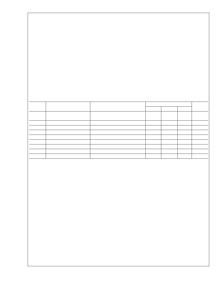
Electrical Characteristics
(See Figure 2 for Test Circuit)
Unless otherwise noted: V
CC
= 85V, V
BB
= 8V, C
L
= 8pF, T
C
= 50∞C
DC Tests: V
IN
= 2.35VDC
AC Tests: Output = 40V
P-P
(35V≠75V) at 1MHz
Symbol
Parameter
Conditions
LM2471
Units
Min
Typical
Max
I
CC
Supply Current
All Three Channels, No AC Input
Signal, No Output Load
60
mA
I
BB
Bias Current
All Three Channels
32
mA
V
OUT
DC Output Voltage
No AC Input Signal, V
IN
= 1.10V
73
78
83
V
DC
A
V
DC Voltage Gain
No AC Input Signal
-24
-27
-30
A
V
Gain Matching
(Note 4), No AC Input Signal
1.0
dB
LE
Linearity Error
(Notes 4, 5), No AC Input Signal
5
%
t
R
Rise Time
(Note 6), 10% to 90%
4.0
ns
t
F
Fall Time
(Note 6), 90% to 10%
4.0
ns
OS
Overshoot
(Note 6)
5
%
Note 1: Absolute Maximum Ratings indicate limits beyond which damage to the device may occur.
Note 2: Operating ratings indicate conditions for which the device is functional, but do not guarantee specific performance limits. For guaranteed specifications and
test conditions, see the Electrical Characteristics. Datasheet min/max specification limits are guaranteed by design, test, or statistical analysis. The guaranteed
specifications apply only for the test conditions listed. Some performance characteristics may change when the device is not operated under the listed test
conditions.
Note 3: All voltages are measured with respect to GND, unless otherwise specified.
Note 4: Calculated value from Voltage Gain test on each channel.
Note 5: Linearity Error is the variation in dc gain from V
IN
= 1.1V to V
IN
= 3.6V.
Note 6: Input from signal generator: t
r
, t
f
<
1 ns.
Note 7: Datasheet min/max specification limits are guaranteed by design, test, or statistical analysis.
LM2471
www.national.com
2
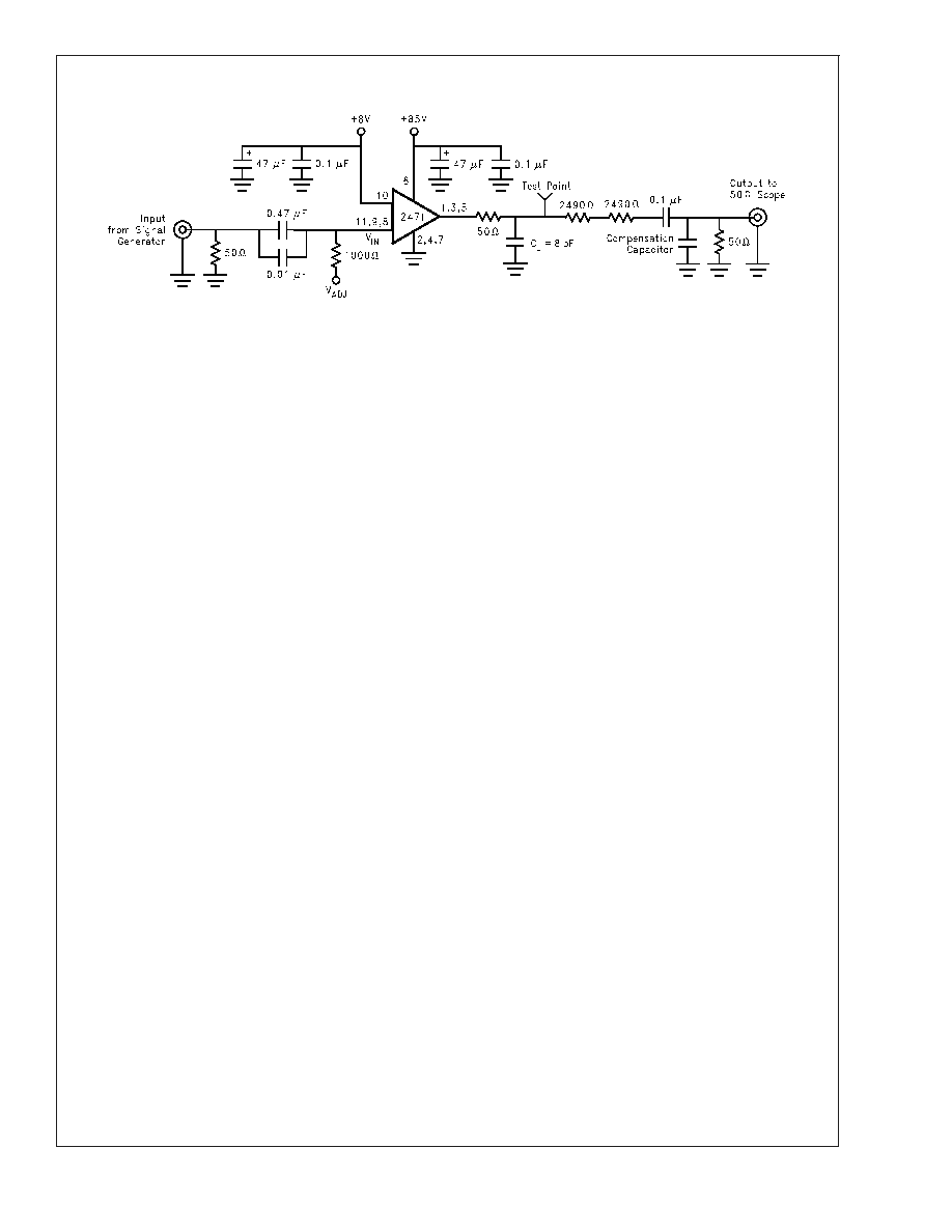
AC Test Circuit
Figure 2 shows a typical test circuit for evaluation of the LM2471. This circuit is designed to allow testing of the LM2471 in a 50
environment without the use of an expensive FET probe. The two 2490
resistors form a 200:1 divider with the 50 resistor and
the oscilloscope. A test point is included for easy use of an oscilloscope probe. The compensation capacitor is used to
compensate the stray capacitance of the two 2490
resistors to achieve flat frequency response.
20103703
Note: 8 pF load includes parasitic capacitance.
FIGURE 2. Test Circuit (One Channel)
LM2471
www.national.com
3

Typical Performance Characteristics
(V
CC
= 85V
DC
, V
BB
= 8V
DC
, C
L
= 8pF, V
OUT
= 40V
P-P
(35V-75V), Test Circuit - Figure 2 unless otherwise specified)
20103704
FIGURE 3. V
OUT
vs V
IN
20103705
FIGURE 4. Speed vs Temp.
20103706
FIGURE 5. LM2471 Pulse Response
20103707
FIGURE 6. Power Dissipation vs Frequency
20103708
FIGURE 7. Speed vs Offset
20103709
FIGURE 8. Speed vs Load Capacitance
LM2471
www.national.com
4

Theory of Operation
The LM2471 is a high voltage monolithic three channel CRT
driver suitable for high resolution display applications. The
LM2471 operates with 85V and 8V power supplies. The part
is housed in the industry standard 11-lead TO-220 molded
plastic power package.
The circuit diagram of the LM2471 is shown in Figure 1. The
PNP emitter follower, Q5, provides input buffering. Q1 and
Q2 form a fixed gain cascode amplifier with resistors R1 and
R2 setting the gain at -27. Emitter followers Q3 and Q4
isolate the high output impedance of the cascode stage from
the capacitance of the CRT cathode which decreases the
sensitivity of the device to load capacitance. Q6 provides
biasing to the output emitter follower stage to reduce cross-
over distortion at low signal levels.
Figure 2 shows a typical test circuit for evaluation of the
LM2471. This circuit is designed to allow testing of the
LM2471 in a 50
environment without the use of an expen-
sive FET probe. In this test circuit, the two 2.49k
resistors
form a 200:1 wideband, low capacitance probe when con-
nected to a 50
coaxial cable and a 50 load (such as a
50
oscilloscope input). The input signal from the generator
is ac coupled to the base of Q5.
Application Hints
INTRODUCTION
National Semiconductor (NSC) is committed to provide ap-
plication information that assists our customers in obtaining
the best performance possible from our products. The fol-
lowing information is provided in order to support this com-
mitment. The reader should be aware that the optimization of
performance was done using a specific printed circuit board
designed at NSC. Variations in performance can be realized
due to physical changes in the printed circuit board and the
application. Therefore, the designer should know that com-
ponent value changes may be required in order to optimize
performance in a given application. The values shown in this
document can be used as a starting point for evaluation
purposes. When working with high bandwidth circuits, good
layout practices are also critical to achieving maximum per-
formance.
IMPORTANT INFORMATION
The LM2471 performance is targeted for the VGA (640 x
480) to UXGA (1600 x 1200, 70Hz) resolution market. The
application circuits shown in this document to optimize per-
formance and to protect against damage from CRT arcover
are designed specifically for the LM2471. If another member
of the LM247X family is used, please refer to its datasheet.
POWER SUPPLY BYPASS
Since the LM2471 is a wide bandwidth amplifier, proper
power supply bypassing is critical for optimum performance.
Improper power supply bypassing can result in large over-
shoot, ringing or oscillation. 0.1 µF capacitors should be
connected from the supply pins, V
CC
and V
BB
, to ground, as
close to the LM2471 as is practical. Additionally, a 47 µF or
larger electrolytic capacitor should be connected from both
supply pins to ground reasonably close to the LM2471.
ARC PROTECTION
During normal CRT operation, internal arcing may occasion-
ally occur. Spark gaps, in the range of 200V, connected from
the CRT cathodes to CRT ground will limit the maximum
voltage, but to a value that is much higher than allowable on
the LM2471. This fast, high voltage, high energy pulse can
damage the LM2471 output stage. The application circuit
shown in Figure 9 is designed to help clamp the voltage at
the output of the LM2471 to a safe level. The clamp diodes,
D1 and D2, should have a fast transient response, high peak
current rating, low series impedance and low shunt capaci-
tance. FDH400 or equivalent diodes are recommended. Do
not use 1N4148 diodes for the clamp diodes. D1 and D2
should have short, low impedance connections to V
CC
and
ground respectively. The cathode of D1 should be located
very close to a separately decoupled bypass capacitor (C3 in
Figure 9). The ground connection of D2 and the decoupling
capacitor should be very close to the LM2471 ground. This
will significantly reduce the high frequency voltage transients
that the LM2471 would be subjected to during an arcover
condition. Resistor R2 limits the arcover current that is seen
by the diodes while R1 limits the current into the LM2471 as
well as the voltage stress at the outputs of the device. R2
should be a
1
/
2
W solid carbon type resistor. R1 can be a
1
/
4
W
metal or carbon film type resistor. Having large value resis-
tors for R1 and R2 would be desirable, but this has the effect
of increasing rise and fall times. Inductor L1 is critical to
reduce the initial high frequency voltage levels that the
LM2471 would be subjected to. The inductor will not only
help protect the device but it will also help minimize rise and
fall times as well as minimize EMI. For proper arc protection,
it is important to not omit any of the arc protection compo-
nents shown in Figure 9.
LM2471
www.national.com
5