LM2476
Monolithic Triple Channel 6.5 ns High Gain CRT Driver
and Bias Clamp
General Description
The LM2476 is a monolithic triple channel CRT driver and
triple bias clamp for low-cost color monitor applications. The
highly integrated IC contains three wide-band amplifiers for
driving the RGB cathodes of a CRT through external cou-
pling capacitors and three low-band clamp amplifiers for DC
restoration and cutoff adjustment of the video outputs. The
CRT drivers have a high, fixed gain of -27 and can drive CRT
capacitive loads as well as resistive loads present in other
applications, limited only by the package's power dissipation.
The IC is packaged in a 19-lead TO-247 molded plastic
package and must be operated with a properly chosen heat
sink. See the Package Mounting and Thermal Consider-
ations sections for more information.
Features
n
Well-matched to the LM123X/4X family of preamplifiers
n
Operates with V
CC
= 60V to 90V
n
Convenient TO-247 staggered lead package style
CRT Drivers
n
High gain of �27 for up to 60V
P-P
output swing
n
Stable with capacitive loads and inductive peaking
networks
Bias Clamps
n
Gain of �17 for up to 60V DC output range
Applications
n
1024 x 768 displays up to 85 Hz refresh rate
n
Pixel clock frequencies up to 95 MHz
n
Monitors using video blanking
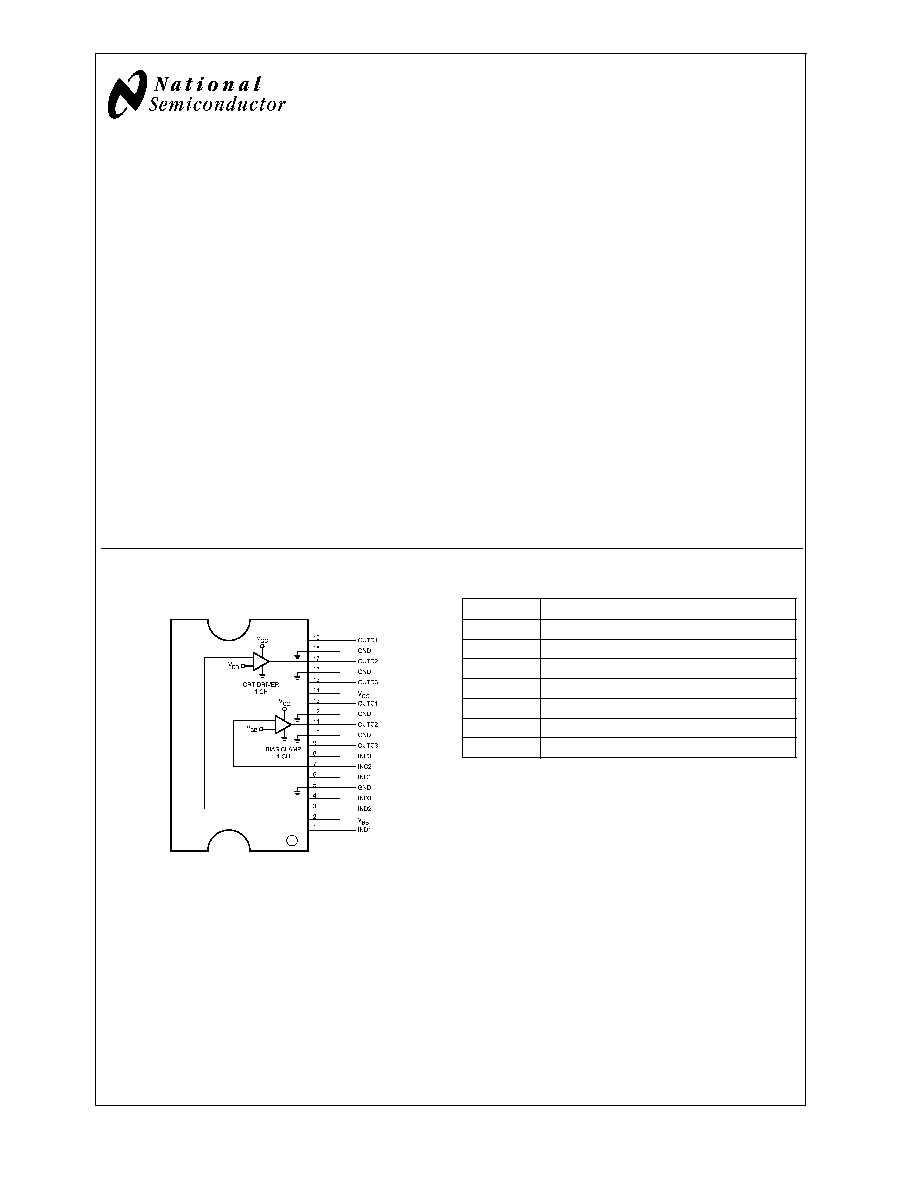
Pinout Diagram and Pin Descriptions
Pin Name
Pin Description
IND
Driver Input Pins (1, 3, 4)
INC
Clamp Input Pins (6, 7, 8)
V
BB
Bias Voltage Pin (2)
V
CC
Supply Voltage Pin (14)
GND*
Ground Pins (5, 10, 12, 16, 18)
OUTC
Clamp Output Pins (9, 11, 13)
OUTD
Driver Output Pins (15, 17, 19)
*Note: All GND pins should be connected together via low HF impedance
traces on the PCB.
20121901
Note: Tab is at GND
FIGURE 1. Pinout and Connection Diagram
January 2004
LM2476
Monolithic
T
riple
Channel
6.5
ns
High
Gain
CRT
Driver
and
Bias
Clamp
� 2005 National Semiconductor Corporation
DS201219
www.national.com
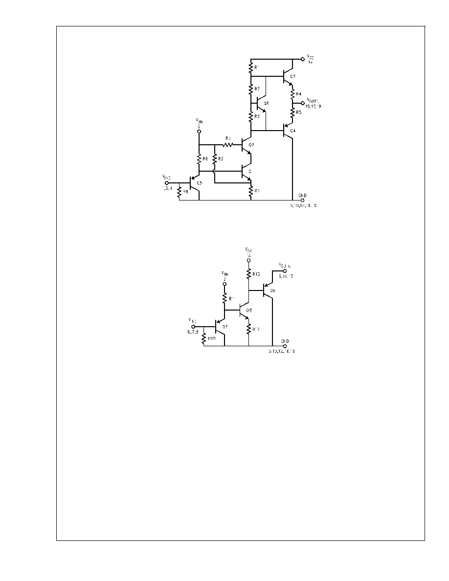
Schematic Diagrams
20121902
FIGURE 2. CRT Driver Simplified Schematic (One Channel)
20121915
FIGURE 3. Bias Clamp Simplified Schematic (One Channel)
LM2476
www.national.com
2
Absolute Maximum Ratings
(Notes 1,
3)
If Military/Aerospace specified devices are required,
please contact the National Semiconductor Sales Office/
Distributors for availability and specifications.
Supply Voltage (V
CC
)
96V
Bias Voltage (V
BB
)
10V
Driver Input Voltage (V
IND
)
0V to 4.5V
Clamp Input Voltage (V
INC
)
0V to 5.0V
Storage Temperature Range (T
STG
)
-65�C to +150�C
Lead Temperature
(Soldering,
<
10 sec.)
300�C
ESD Tolerance
Human Body Model
2 KV
Machine Model
200V
Operating Ranges
(Note 2)
V
CC
60V to 85V
V
BB
7V to 9V
V
IND
0V to 3.5V
V
INC
0V to 4.0V
V
OUTD
(Driver Output Voltage)
12V to V
CC
V
OUTC
(Clamp Output Voltage)
12V to V
CC
Case Temperature (device tab)
-20�C to +100�C
Do not operate the part without a heat sink.
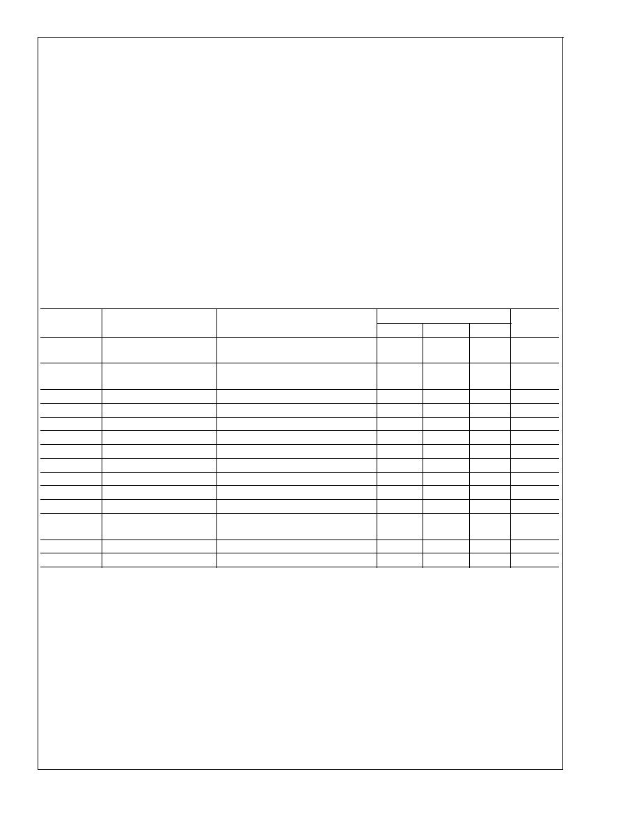
Electrical Characteristics
(See Figure 4 for Test Circuit)
Unless otherwise noted: V
CC
= 85V, V
BB
= 8V, C
L
= 8 pF, T
C
= 40�C
DC Tests: V
IND
= 2.30V, V
INC
= 2.35V
AC Tests: V
OUTD
= 40V
P-P
(35V � 75V) at 1 MHz, V
INC
= 2.35V
Symbol
Parameter
Conditions
LM2476
Units
Min
Typical
Max
I
CC
Supply Current
All Three Channels, No AC Input
Signal, No Output Load
34
45
mA
I
BB
Bias Current
All Three Channels, No AC Input
Signal, No Output Load
21
30
mA
V
OUTD, 1
Driver DC Output Voltage
No AC Input Signal, V
IND
= 2.30V
41
46
51
V
V
OUTD, 2
Driver DC Output Voltage
No AC Input Signal, V
IND
= 1.15V
72
77
82
V
A
V-OUTD
Driver DC Voltage Gain
No AC Input Signal
�24
�27
�30
A
V-OUTD
Driver Gain Matching
(Note 4), No AC Input Signal
1.0
dB
LE
OUTD
Driver Linearity Error
(Notes 4, 5), No AC Input Signal
5
%
t
R
Rise Time
(Note 6), 10% to 90%
6.0
ns
t
F
Fall Time
(Note 6), 90% to 10%
6.7
ns
OS
Overshoot
(Note 6)
3
%
V
OUTC
Clamp DC Output Voltage
V
INC
= 2.35V
46
51
56
V
V
OUTC-RANGE
Clamp DC Output Voltage
Range
V
INC-RANGE
= 0.5V to 4.0V
58
VDC
A
V-OUTC
Clamp DC Voltage Gain
No AC Input Signal
�14.5
�16.5
�18.5
LE
OUTC
Clamp Linearity Error
(Notes 4, 5), No AC Input Signal
5
%
Note 1: Absolute Maximum Ratings indicate limits beyond which damage to the device may occur.
Note 2: Operating ratings indicate conditions for which the device is functional, but do not guarantee specific performance limits. For guaranteed specifications and
test conditions, see the Electrical Characteristics. Datasheet min/max specification limits are guaranteed by design, test, or statistical analysis. The guaranteed
specifications apply only for the test conditions listed. Some performance characteristics may change when the device is not operated under the listed test
conditions.
Note 3: All voltages are measured with respect to GND, unless otherwise specified.
Note 4: Calculated value from Voltage Gain test on each channel.
Note 5: Driver Linearity Error is the variation in dc gain from V
IND
= 1.1V to V
IND
= 3.6V.
Note 6: Input from signal generator: t
r
, t
f
<
1 ns.
Note 7: Clamp Linearity Error is the variation in dc gain from V
INC
= 1.0V to V
INC
= 4.0V.
LM2476
www.national.com
3

LM2476 Test Circuits
Figure 4 shows a typical test circuit to evaluate the LM2476 CRT Driver and Bias Clamp electrical characteristics. The driver test
circuit is designed to allow for testing the transient response in a 50
environment without the use of an expensive FET probe.
An input from a 50
pulse generator output can be AC coupled and biased with an external supply via the V
BIAS
input. The two
2.49 k
resistors form a 200:1 divider with the 50 resistor and the oscilloscope. The clamp test circuit is designed to allow for
testing the clamp outputs. A clamp input can be biased with an external supply via the V
DC
input and a high impedance voltmeter
(
>
100M
) can be used to measure the DC voltage at the clamp outputs. Test points can included to accommodate voltmeter or
oscilloscope probes.
20121903
Note: 8 pF load includes parasitic capacitance.
FIGURE 4. CRT Driver and Bias Clamp Test Circuits (One Channel)
LM2476
www.national.com
4
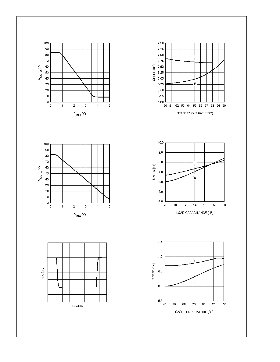
Typical Performance Characteristics
(V
CC
= 85V, V
BB
= 8V, C
L
= 8 pF, V
OUTD
= 40V
P-P
(35V -
75V), V
INC
= 2.35V, Test Circuit - Figure 4 unless otherwise specified)
20121904
FIGURE 5. V
OUTD
vs V
IND
20121917
FIGURE 6. V
OUTC
vs V
INC
20121906
FIGURE 7. LM2476 Pulse Response
20121908
FIGURE 8. Speed vs Offset
20121909
FIGURE 9. Speed vs Load Capacitance
20121905
FIGURE 10. Speed vs Temperature
LM2476
www.national.com
5