LM2483
180V Triple Bias Clamp
General Description
The LM2483 driver is an Integrated 180V triple bias clamp
circuit for DC recovery of each of the AC coupled outputs of
a HDTV CRT driver. It is well matched with the DAC outputs
of the LM126X family of pre-amplifiers. Each amplifier has its
gain internally set to -30. The LM2483 is packaged in an
industry standard 14 lead molded plastic dual-in-line pack-
age.
Features
n
Wide range integrated triple bias clamp
n
High input impedance
n
Matched to LM2426 HDTV Driver
Applications
n
AC coupled HDTV applications using the 1080i and
720p formats as well as standard NTSC and PAL
formats.
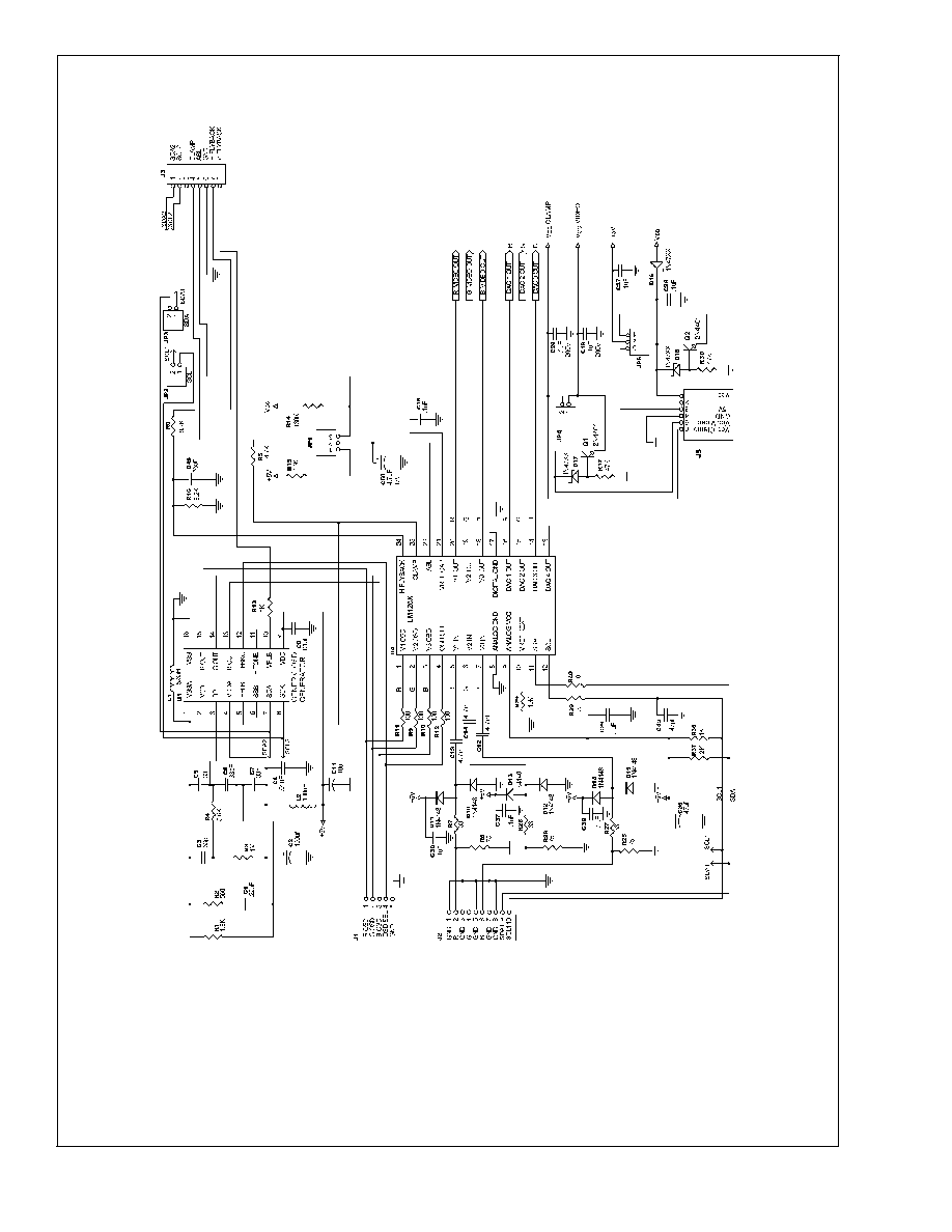
Schematic and Connection Diagrams
20052933
Top View
Order Number LM2483NA
20052932
FIGURE 1. Simplified Schematic Diagram (One
Channel)
November 2002
LM2483
180V
T
riple
Bias
Clamp
© 2002 National Semiconductor Corporation
DS200529
www.national.com
Absolute Maximum Ratings
(Notes 1,
3)
If Military/Aerospace specified devices are required,
please contact the National Semiconductor Sales Office/
Distributors for availability and specifications.
Supply Voltage, V
CC
+200V
Bias Voltage, V
BB
+15V
Input Voltage, V
IN
-0.5V to V
BB
+0.5V
Storage Temperature Range, T
STG
-65∞C to +150∞C
Lead Temperature (Soldering,
<
10sec.)
300∞C
ESD Tolerance
Machine Model
200V
Human Body Model
1.5 kV
Max Junction Temperature
150∞C
JA
(Typ) (Note 5)
70∞C
Limits of Operating Ranges
(Note 3)
V
CC
130V to 180V
V
BB
7V to 13V
V
IN
1V to 5V
V
OUT
40V to 175V
Ambient Temperature Range, T
A
0∞C to 70∞C
DC Clamp Electrical Characteristics
(See Figure 2 for Test Circuit)
Unless otherwise noted: V
CC
= +180V, V
BB
= 8V, V
IN
= +2.5V, T
A
= 30∞C
Symbol
Parameter
Conditions
Min
Typ
Max
Units
I
CC
Supply Current
All three channels, includes 100K
pull-up resistor current
4.5
7
mA
I
BB
Bias Supply Current
All channels
4
mA
V
OUT
DC Output Voltage
122
127
132
V
DC
V
OUT-Range
Output Voltage Range
V
IN
Range = +1.5V to 4.5V
89
V
A
V
DC Voltage Gain
-27
-30
-33
V/V
LE
Linearity Error
See Note 4
5
%
Note 1: Absolute Maximum Ratings indicate limits beyond which damage to the device may occur.
Note 2: Operating Ratings indicate conditions for which the device is functional, but do not guarantee specific performance limits. For guaranteed specifications and
the test conditions, see the Electrical Characteristics. Datasheet min/max specification limits are guaranteed by design, test, or statistical analysis. The guaranteed
specifications apply only for the test conditions listed. Some performance characteristics may change when the device is not operated under the listed test
conditions.
Note 3: All voltages are measured with respect to GND, unless otherwise specified.
Note 4: Linearity Error is the variation in dc gain from V
IN
= 1.5 volts to V
IN
= 4.5 volts.
Note 5: Measured with 1in
2
copper on PCB connected to pins 3, 4, 5, 10, 11, 12. See Thermal Considerations Section.
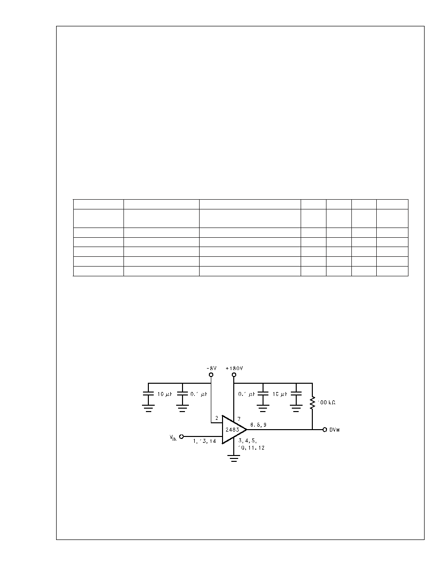
Test Circuit
Figure 2 shows the test circuit for evaluation of the LM2483 Clamp Amplifier. A high impedance Voltmeter (
>
100M
) is used for
DC measurements at the output.
20052934
FIGURE 2. Test Circuit
LM2483
www.national.com
2
Typical Performance Characteristics
(V
CC
= +180V, V
BB
= +8V, V
IN
= +2.5V, Test Circuit - Figure 2)
Theory of Operation
The simplified circuit diagram of the LM2483 is shown in
Figure 1. The DC clamp circuit amplifies the input signal by
-30 and the gain is set by the resistor ratio of 30R and R. The
output will require a pull-up resistor to 180V.
Figure 2 shows the test circuit for evaluation of the LM2483
Clamp Amplifier. A high impedance voltmeter (
>
100M
) is
used for DC measurements at the output.
Application Hints
INTRODUCTION
National Semiconductor (NSC) is committed to provide ap-
plication information that assists our customers in obtaining
the best performance possible from our products. The fol-
lowing information is provided in order to support this com-
mitment. The reader should be aware that the optimization of
performance was done using a specific printed circuit board
designed at NSC. Variations in performance can be realized
due to physical changes in the printed circuit board and the
application. Therefore, the designer should know that com-
ponent value changes may be required in order to optimize
performance in a given application. The values shown in this
document can be used as a starting point for evaluation
purposes.
POWER SUPPLY BYPASS
The LM2483 should have proper power supply bypassing for
optimum performance. A 0.1 µF capacitor should be con-
nected from the supply pins, V
CC
and V
BB
, to ground, as
close to the supply and ground pins as is practical. Addition-
ally, a 1 µF electrolytic capacitor should be connected from
the supply pins to ground. The electrolytic capacitor should
also be placed reasonably close to the LM2483's supply and
ground pins.
ARC PROTECTION
During normal CRT operation, internal arcing may occasion-
ally occur. To protect the LM2483 against arcing the follow-
ing steps should be done (See Figure 7):
∑
The traces connecting the LM126X preamp DACs and
the LM2483 input pins (pins 1, 13, and 14) should be run
around the top of the LM2426. They should not go
through the output circuit of the LM2426.
∑
C43, C44, and C45 should be located close to the
LM126X preamp.
∑
R44, R45, and R46 should be located close to the
LM2483.
∑
C21, C24, and C25 on the output pins of the LM2483
(pins 6, 8, and 9) should be located close to the LM2483.
The grounds of these capacitors should have a short
direct return to GND (pins 3, 4, 5, 10, 11, and 12) of the
LM2483.
∑
C9 and C36 on the supply lines (pins 2 and 7) should be
located close to the LM2483. The grounds of these ca-
pacitors should have a short direct return to GND (pins 3,
4, 5, 10, 11, and 12) of the LM2483.
∑
The ground of the LM2483 should have a short direct
connection to the ground of the LM2426.
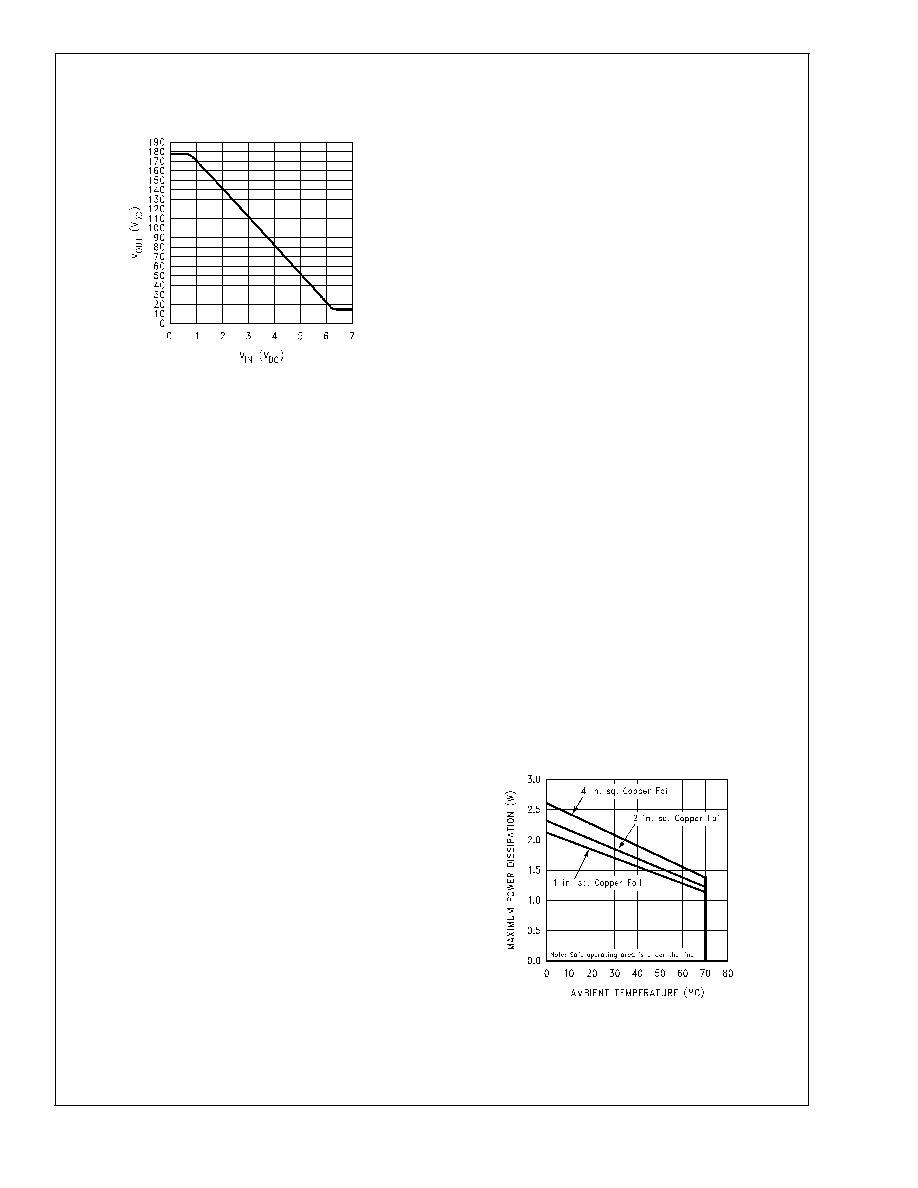
Thermal Considerations
The package the LM2483 is in uses the ground pins (3, 4, 5,
10, 11, and 12) to conduct heat from the LM2483. These pins
should be connected to a ground plane that acts as a heat
sink. See the example ground plane connected to these pins
in the National Semiconductor PCB shown in Figure 7.
Figure 4 is used to determine the size of ground plane heat
sink. The lines in Figure 4 represent a junction temperature
of 150∞C when the size of heat sink noted by the line is used.
The area under the line is the safe operating area. Using
Figure 4, the following example shows how to determine the
size of the ground plane.
The LM2483 uses about 0.45W of quiescent power. If V
CC
=
+180V, and each channel of the LM2483 needs to sink an
average of 1mA, the LM2483 will use:
0.45W + 3 x (180V x 1mA ) = 0.99W
Figure 4 shows that the LM2483 dissipating 0.99W with one
sq. in. of copper ground plane heat sink is in the safe
operating range for any ambient temperature up to 70∞C.
20052935
FIGURE 3. V
out
vs V
in
20052936
FIGURE 4. Maximum Power Dissipation vs. Ambient
Temperature
LM2483
www.national.com
3