LM25005
42V, 2.5A Step-Down Switching Regulator
General Description
The LM25005 switching regulator features all of the func-
tions necessary to implement an efficient, high voltage buck
regulator using a minimum of external components. This
easy to use regulator includes a 42V, 160m
, N-channel
MOSFET, with an output current capability of 2.5 Amps. The
regulator control method is based upon current mode control
utilizing an emulated current ramp. Current mode control
provides inherent line voltage feed-forward, cycle-by-cycle
current limiting and ease of loop compensation. The use of
an emulated control ramp reduces noise sensitivity of the
pulse-width modulation circuit, allowing reliable control of
very small duty cycles necessary in high input voltage appli-
cations. The operating frequency is programmable from
50kHz to 500kHz. An oscillator synchronization pin allows
multiple LM25005 regulators to self-synchronize or to be
synchronized to an external clock. Additional protection fea-
tures include: current limit, thermal shutdown and remote
shutdown capability. The device is available in a power
enhanced TSSOP-20 package featuring an exposed die
attach pad to aid thermal dissipation.
Features
n
Integrated 42V, 160m
N-channel MOSFET
n
Ultra-wide input voltage range from 7V to 42V
n
Internal bias regulator
n
Adjustable output voltage from 1.225V
n
1.5% feedback reference accuracy
n
Current mode control with emulated inductor current
ramp
n
Single resistor oscillator frequency setting
n
Oscillator synchronization input
n
Programmable soft-start
n
Shutdown / Standby input
n
Wide bandwidth error amplifier
n
Thermal Shutdown
Package
n
TSSOP-20EP (Exposed Pad)
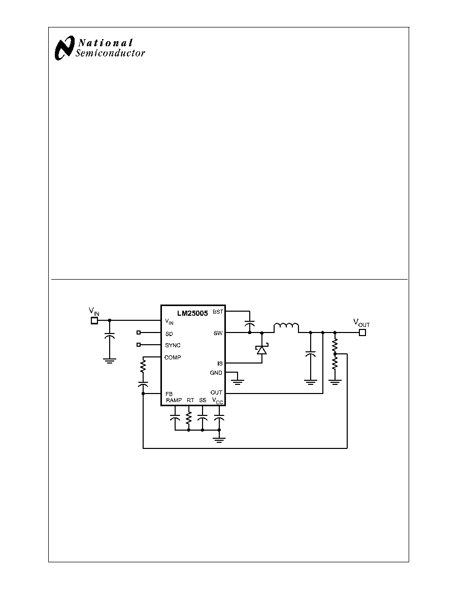
Simplified Application Schematic
20170001
February 2006
LM25005
42V
,
2.5A
Step-Down
Switching
Regulator
© 2006 National Semiconductor Corporation
DS201700
www.national.com
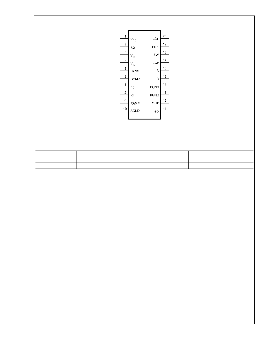
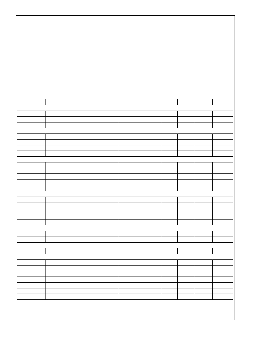
Pin Descriptions
Pin(S)
Name
Description
Application Information
1
VCC
Output of the bias regulator
Vcc tracks Vin up to 9V. Beyond 9V, Vcc is regulated to
7 Volts. A 0.1uF to 1uF ceramic decoupling capacitor is
required. An external voltage (7.5V ≠ 14V) can be
applied to this pin to reduce internal power dissipation.
2
SD
Shutdown or UVLO input
If the SD pin voltage is below 0.7V the regulator will be in
a low power state. If the SD pin voltage is between 0.7V
and 1.225V the regulator will be in standby mode. If the
SD pin voltage is above 1.225V the regulator will be
operational. An external voltage divider can be used to
set a line undervoltage shutdown threshold. If the SD pin
is left open circuit, a 5µA pull-up current source
configures the regulator fully operational.
3, 4
Vin
Input supply voltage
Nominal operating range: 7V to 42V
5
SYNC
Oscillator synchronization input or
output
The internal oscillator can be synchronized to an external
clock with an external pull-down device. Multiple
LM25005 devices can be synchronized together by
connection of their SYNC pins.
6
COMP
Output of the internal error amplifier
The loop compensation network should be connected
between this pin and the FB pin.
7
FB
Feedback signal from the regulated
output
This pin is connected to the inverting input of the internal
error amplifier. The regulation threshold is 1.225V.
8
RT
Internal oscillator frequency set input
The internal oscillator is set with a single resistor,
connected between this pin and the AGND pin. The
recommended frequency range is 50KHz to 500KHz.
9
RAMP
Ramp control signal
An external capacitor connected between this pin and the
AGND pin sets the ramp slope used for current mode
control. Recommended capacitor range 50pF to 2000pF.
10
AGND
Analog ground
Internal reference for the regulator control functions
11
SS
Soft-start
An external capacitor and an internal 10µA current
source set the time constant for the rise of the error amp
reference. The SS pin is held low during standby, Vcc
UVLO and thermal shutdown.
12
OUT
Output voltage connection
Connect directly to the regulated output voltage.
13, 14
PGND
Power ground
Low side reference for the PRE switch and the IS sense
resistor.
15, 16
IS
Current sense
Current measurement connection for the re-circulating
diode. An internal sense resistor and a sample/hold
circuit sense the diode current near the conclusion of the
off-time. This current measurement provides the DC level
of the emulated current ramp.
17, 18
SW
Switching node
The source terminal of the internal buck switch. The SW
pin should be connected to the external Schottky diode
and to the buck inductor.
19
PRE
Pre-charge assist for the bootstrap
capacitor
This open drain output can be connected to SW pin to
aid charging the bootstrap capacitor during very light load
conditions or in applications where the output may be
pre-charged before the LM25005 is enabled. An internal
pre-charge MOSFET is turned on for 250ns each cycle
just prior to the on-time interval of the buck switch.
LM25005
www.national.com
3
Absolute Maximum Ratings
(Note 1)
If Military/Aerospace specified devices are required,
please contact the National Semiconductor Sales Office/
Distributors for availability and specifications.
V
IN
to GND
45V
BST to GND
60V
PRE to GND
45V
SW to GND (Steady State)
-1.5V
BST to V
CC
45V
V
CC
to GND
14V
BST to SW
14V
OUT to GND
Limited to Vin
SD, SYNC, SS, FB to GND
7V
ESD Rating (Note 2)
Human Body Model
2kV
Storage Temperature Range
-65∞C to +150∞C
Operating Ratings
(Note 1)
V
IN
7V to 42V
Operation Junction Temperature
-40∞C to + 125∞C
Electrical Characteristics
Specifications with standard typeface are for T
J
= 25∞C, and those with boldface
type apply over full Operating Junction Temperature range. V
IN
= 24V, R
T
= 32.4k
unless otherwise stated. (Note 3)
Symbol
Parameter
Conditions
Min
Typ
Max
Units
STARTUP REGULATOR
VccReg
Vcc Regulator Output
6.85
7.15
7.45
V
Vcc LDO Mode turn-off
9
V
Vcc Current Limit
Vcc = 0V
20
mA
VCC SUPPLY
Vcc UVLO Threshold
(Vcc increasing)
5.95
6.35
6.75
V
Vcc Undervoltage Hysteresis
1
V
Bias Current (Iin)
FB = 1.3V
3
4.5
mA
Shutdown Current (Iin)
SD = 0V
50
85
µA
SHUTDOWN THRESHOLDS
Shutdown Threshold
(SD Increasing)
0.5
0.7
0.9
V
Shutdown Hysteresis
0.1
V
Standby Threshold
(Standby Increasing)
1.18
1.225
1.27
V
Standby Hysteresis
0.1
V
SD Pull-up Current Source
5
µA
SWITCH CHARACTERSICS
Buck Switch Rds(on)
160
320
m
BOOST UVLO
3.8
V
BOOST UVLO Hysteresis
0.56
V
Pre-charge Switch Rds(on)
75
Pre-charge Switch on-time
275
ns
CURRENT LIMIT
Cycle by Cycle Current Limit
RAMP = 0V
3
3.5
4.25
A
Cycle by Cycle Current Limit Delay
RAMP = 2.5V
100
ns
SOFT-START
SS Current Source
7
10
14
µA
OSCILLATOR
Frequency1
180
200
220
KHz
Frequency2
RT = 11k
425
485
525
KHz
SYNC Source Impedance
10
k
SYNC Sink Impedance
160
SYNC Threshold (falling)
1.4
V
Upper SYNC Frequency
550
KHz
SYNC Pulse Width Minimum
15
ns
LM25005
www.national.com
5