 | –≠–ª–µ–∫—Ç—Ä–æ–Ω–Ω—ã–π –∫–æ–º–ø–æ–Ω–µ–Ω—Ç: LM2501 | –°–∫–∞—á–∞—Ç—å:  PDF PDF  ZIP ZIP |
LM2501
Mobile Pixel Link (MPL) Camera Interface Serializer and
Deserializer
General Description
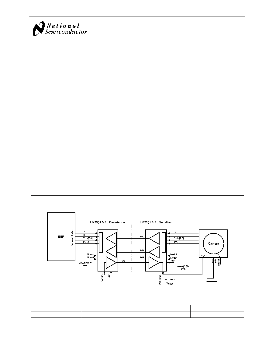
The LM2501 device is a Serializer/Deserializer that adapts
existing video busses to Mobile Pixel Link (MPL). MPL is
intended to replace wide LVCMOS video interfaces inside
portable electronics equipment benefiting their cost, size,
EMI and power consumption.
By using the LM2501 SERDES chipset, the interconnect is
reduced from 12 active signals to only 3 active signals
providing a 75% reduction. This eases interconect and flex
design, size and cost.
Contained in a 24 lead Ultra Thin CSP Package, the Serial-
izer resides beside the video source (camera) and translates
the parallel bus from LVCMOS levels to serial MPL levels for
transmission over a flex cable to the Deserializer located by
the respective destination Video Input Port.
An extra clock transport is provided to deliver a clock signal
to the target. For example, from the main board to the flip
board where the camera module is located. Transmission of
the clock also benefits from MPL's low power transmission
and low EMI.
The Power_Down (PD*) input controls the power state of the
MPL interface. When PD* is asserted, the MD, MC and WC
signals are powered down to save current and reduce power
dissipation.
Features
n
160 Mbps Raw Throughput
n
MPL-0 Meets MPL Physical Layer Specification
n
Configurable as a Serializer or Deserializer
n
Complete LVCMOS to MPL Translation
n
Serializes 8-bit Camera Interface
-- 8-bit color data
-- plus VSYNC and HSYNC bits
n
Link power down mode reduces quiescent power under
10 µA (actual TBD)
n
1.7V≠3.1V and 2.9-3.1V Supply Voltage
n
Interfaces to 1.8V≠3.0V Logic
n
Offered in a small 24L UCSP Package
-- 3.5 mm X 4.5 mm
-- 0.6 mm Max Height
System Benefits
n
Reduced Wire Interface
n
Low Power
n
Low EMI
n
Extra Clock Transport
n
Intrinsic Level Translation
Typical Application Diagram
20091601
Ordering Information
NSID
Package Type
Package ID
LM2501SL
24-Lead Ultra Thin CSP 3.5 X 4.5 X 0.6 mm
SLE24A
I2C
Æ
is a registered trademark of Phillips Corporation.
ADVANCE INFORMATION
June 2004
LM2501
Mobile
Pixel
Link
(MPL)
Camera
Interface
Serializer
and
Deserializer
© 2004 National Semiconductor Corporation
DS200916
www.national.com
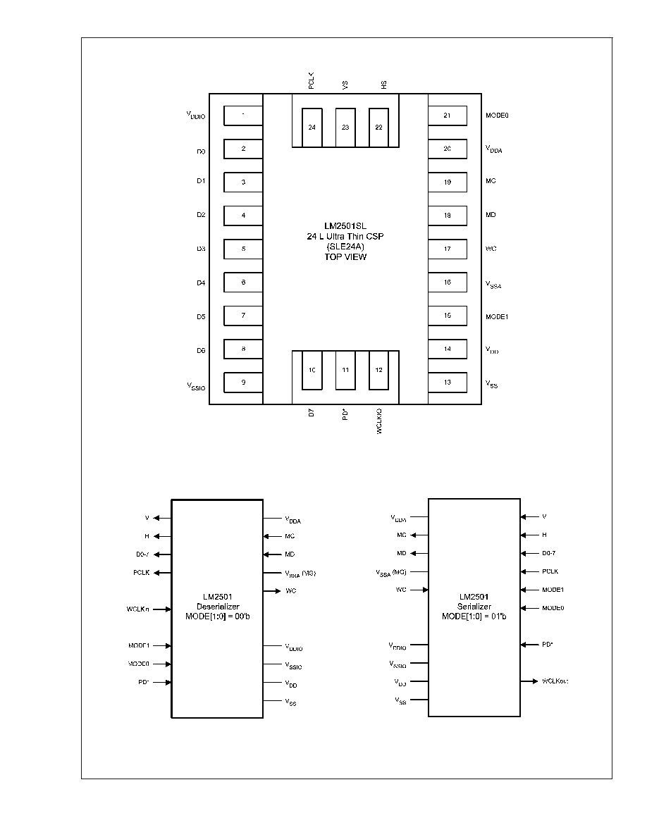
Connection Diagram
20091612
TOP VIEW
General Block Diagrams: Serializer and Deserializer
20091613
LM2501
www.national.com
2
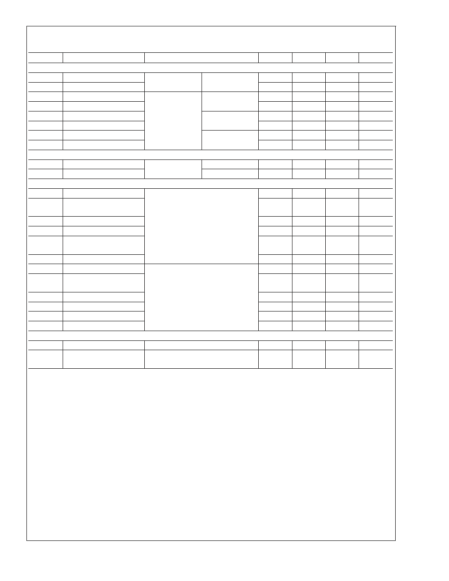
Pin Description
Pin Name
No.
of Pins
I/O, Type
Description
MPL SERIAL BUS PINS
MD
1
IO, MPL
MPL Data line. Serializer is a Line Driver. Deserializer is a Receiver. Configured by
the Mode[1:0] pins.
MC
1
IO, MPL
MPL Clock line. Serializer is a Line Driver. Deserializer is a Receiver. Configured by
the Mode[1:0] pins.
MG
1
Ground
See VSSA below.
CONFIGURATION/PARALLEL BUS PINS
Mode[1:0]
2
I, LVCMOS
Mode Configuration Input pins:
Mode[1:0], NOTE - Applies to REV F/G Samples only.
00
: Deserializer
01
: Serializer with PD* input
10
: Reserved
11
: Reserved
PD*
1
I, LVCMOS
Power_Down. Input pin. Active Low. When PD* is Low the device is in the sleep
state.
D0≠D7
8
IO, LVCMOS
8-bit Bi-directional Data Bus ≠ Serializer Input, Deserializer Output
VS
1
IO, LVCMOS
VSYNC ≠ Serializer Input, Deserializer Output
HS
1
IO, LVCMOS
HSYNC ≠ Serializer Input, Deserializer Output
PCLK
1
IO, LVCMOS
Pixel Clock. Serializer Input, Deserializer Output
WHISPER CLOCK
WCLKIO
1
IO, LVCMOS
Extra Clock Input for WhisperClock Link ≠ Deserializer Input. Serializer Output.
WC
1
IO, MPL
Extra WhisperClock MPL signal ≠ Serializer is an MPL input signal, Deserializer is
an MPL output signal.
POWER/GROUND PINS
V
DDA
1
Power
Power Supply Pin for the MPL Interface. 3.0V
±
3%
V
SSA
1
Ground
Ground Pin for the MPL Interface, also known as MG (MPL Ground)
V
DD
1
Power
Power Supply Pin for the digital core and Serializer PLL. 3.0V
±
3%
V
SS
1
Ground
Ground Pin for the digital core and Serializer PLL.
V
DDIO
1
Power
Power Supply Pin for the parallel interface. 1.7V to 3.1V
V
SSIO
1
Ground
Ground Pin for the parallel interface.
Notes:
I = Input, O = Output, IO = Input/Output
Do NOT float unused inputs.
ES Revision notes
Rev D/E
Sampled on MPL200EVK
Use prior datasheet edition
Rev F
S/D* and TM pins changed to Mode[1:0]
Use this datasheet edition
Rev G
MPL RX enhancements
LM2501
www.national.com
3
Absolute Maximum Ratings
(Note 1)
If Military/Aerospace specified devices are required,
please contact the National Semiconductor Sales Office/
Distributors for availability and specifications.
Supply Voltage (V
DDA
)
-0.3V to +TBDV
Supply Voltage (V
DD
)
-0.3V to +TBDV
Supply Voltage (V
DDIO
)
-0.3V to +TBDV
LVCMOS Input/Output Voltage
-0.3V to (V
DDIO
+0.3V)
MPL Input/Output Voltage
TBD
Junction Temperature
+150∞C
Storage Temperature
-65∞C to +150∞C
Lead Temperature Soldering,
4 Seconds
+260∞C
ESD Ratings:
HBM, 1.5 k
, 100pF
±
2 kV
EIAJ, 0
, 200 pF
±
200V
Maximum Package Power Dissipation Capacity at 25∞C
24L UCSP Package
TBD W
Derate TBD Package above 25∞C
TBD mW/∞C
Recommended Operating
Conditions
Min Typ
Max
Units
Supply Voltage
V
DDA
to V
SSA
and
V
DD
to V
SS
2.9
3.0
3.1
V
V
DDIO
to V
SSIO
1.7
3.1
V
PLK Clock Frequency
4
16
MHz
WC Clock Frequency
4
28
MHz
Ambient Temperature
0
25
70
∞C
Electrical Characteristics
Over recommended operating supply and temperature ranges unless otherwise specified. (Note 2)
Symbol
Parameter
Conditions
Min
Typ
Max
Units
MPL
I
OLL
Logic Low Current
4.8 I
B
5.0 I
B
5.3 I
B
µA
I
OMS
Mid Scale Current
3.0 I
B
µA
I
OHL
Logic High Current
0.8 I
B
1.0 I
B
1.2 I
B
µA
I
B
Current Bias
150
µA
LVCMOS (1.7V to 3.1V)
V
IH
Input Voltage High Level
0.7 V
DDIO
V
DDIO
+0.3
V
V
IL
Input Voltage Low Level
-0.3
0.3 V
DDIO
V
I
IN
Input Current (includes I
OZ
)
-5
0
+5
µA
I
IH
Input Current High Level
-1
0
+1
µA
I
IL
Input Current Low Level
-1
0
+1
µA
V
OH
Output Voltage High Level
I
OH
= -2 mA
0.8 V
DDIO
V
V
OL
Output Voltage Low Level
I
OL
= 2 mA
0.2 V
DDIO
V
I
OS
Output Short Circuit
Current
V
OUT
= 0V
TBD
mA
SUPPLY CURRENT
I
CC
Total Supply
Current -- Enabled
PCLK = 16MHz
WC = 28MHz
MD = 0101-1010
pattern
C
L
= 15 pF
Serializer
TBD
TBD
µA
Deserializer
TBD
TBD
µA
I
CCZ
Supply Current -- Disable
Power_Down Mode PD* = L
1
10
µA
PD* = L
1
10
µA
LM2501
www.national.com
4
Switching Characteristics
Over recommended operating supply and temperature ranges unless otherwise specified. (Note 2)
Symbol
Parameter
Conditions
Min
Typ
Max
Units
PARALLEL BUS TIMING
t
SET
Set Time - Data to Clock
Inputs
Figure 2
TBD
ns
t
HOLD
Hold Time - Clock to Data
TBD
ns
t
RISE
Rise Time
Outputs,
C
L
= 15 pF
ns
t
FALL
Fall Time
ns
PC
LOW
PCLK Low
50
%
PC
HIGH
PCLK High
50
%
t
DVBC
Data Valid before Clock
Figure 2
TBD
ns
t
DVAC
Data Valid after Clock
TBD
ns
SERIAL BUS TIMING
t
DVBC
Figure 1
t
DVAC
POWER UP TIMING (see Figures 5, 6)
t
1
WC Start Up Delay
Figure 5
Planned Rev G ES test Chip will
double WC cyc counts on T
1
to T
4
(SER) parameters to support higher
WC rates.
100
WC
CYC
t
2
WC Low Initialization Low
State
11
12
13
WC
CYC
t
3
WC Pulse Width High
11
12
13
WC
CYC
t
4
WC Low State
11
12
13
WC
CYC
t
5
WC
IN
to WC
OUT
Latency
(SER)
6
7
8
WC
CYC
t
6
TBD
9
WC
CYC
t
7
SER PLL Lock Time
Figure 6
4,096
MC
CYC
t
8
MC Low Initialization Low
State
11
12
13
MC
CYC
t
9
MC Pulse Width High
11
12
13
MC
CYC
t
10
MC Low State
11
12
13
MC
CYC
t
11
SER Latency
TBD
MC
CYC
t
12
DES Latency
TBD
MC
CYC
POWER OFF TIMING
t
PAZ
Disable Time to Power Off
µs
t
PZA
Enable Time from Power
Off
µs
LM2501
www.national.com
5