LM1577/LM2577 Series
SIMPLE SWITCHER
Æ
Step-Up Voltage Regulator
General Description
The LM1577/LM2577 are monolithic integrated circuits that
provide all of the power and control functions for step-up
(boost), flyback, and forward converter switching regulators.
The device is available in three different output voltage ver-
sions: 12V, 15V, and adjustable.
Requiring a minimum number of external components, these
regulators are cost effective, and simple to use. Listed in this
data sheet are a family of standard inductors and flyback
transformers designed to work with these switching regula-
tors.
Included on the chip is a 3.0A NPN switch and its associated
protection circuitry, consisting of current and thermal limiting,
and undervoltage lockout. Other features include a 52 kHz
fixed-frequency oscillator that requires no external compo-
nents, a soft start mode to reduce in-rush current during
start-up, and current mode control for improved rejection of
input voltage and output load transients.
Features
n
Requires few external components
n
NPN output switches 3.0A, can stand off 65V
n
Wide input voltage range: 3.5V to 40V
n
Current-mode operation for improved transient
response, line regulation, and current limit
n
52 kHz internal oscillator
n
Soft-start function reduces in-rush current during start-up
n
Output switch protected by current limit, under-voltage
lockout, and thermal shutdown
Typical Applications
n
Simple boost regulator
n
Flyback and forward regulators
n
Multiple-output regulator
Typical Application
Ordering Information
Temperature
Range
Package
Type
Output Voltage
NSC
12V
15V
ADJ
Package Package
Drawing
-40∞C
T
A
+125∞C
24-Pin Surface Mount
LM2577M-12
LM2577M-15
LM2577M-ADJ
M24B
SO
16-Pin Molded DIP
LM2577N-12
LM2577N-15
LM2577N-ADJ
N16A
N
5-Lead Surface Mount
LM2577S-12
LM2577S-15
LM2577S-ADJ
TS5B
TO-263
5-Straight Leads
LM2577T-12
LM2577T-15
LM2577T-ADJ
T05A
TO-220
5-Bent Staggered
LM2577T-12
LM2577T-15
LM2577T-ADJ
T05D
TO-220
Leads
Flow LB03
Flow LB03
Flow LB03
-55∞C
T
A
+150∞C
4-Pin TO-3
LM1577K-12/883 LM1577K-15/883
LM1577K-
ADJ/883
K04A
TO-3
SIMPLE SWITCHER
Æ
is a registered trademark of National Semiconductor Corporation.
DS011468-1
Note: Pin numbers shown are for TO-220 (T) package.
June 1999
LM1577/LM2577
Series
SIMPLE
SWITCHER
Step-Up
V
oltage
Regulator
© 1999 National Semiconductor Corporation
DS011468
www.national.com

Absolute Maximum Ratings
(Note 1)
If Military/Aerospace specified devices are required,
please contact the National Semiconductor Sales Office/
Distributors for availability and specifications.
Supply Voltage
45V
Output Switch Voltage
65V
Output Switch Current (Note 2)
6.0A
Power Dissipation
Internally Limited
Storage Temperature Range
-65∞C to +150∞C
Lead Temperature
(Soldering, 10 sec.)
260∞C
Maximum Junction Temperature
150∞C
Minimum ESD Rating
(C = 100 pF, R = 1.5 k
)
2 kV
Operating Ratings
Supply Voltage
3.5V
V
IN
40V
Output Switch Voltage
0V
V
SWITCH
60V
Output Switch Current
I
SWITCH
3.0A
Junction Temperature Range
LM1577
-55∞C
T
J
+150∞C
LM2577
-40∞C
T
J
+125∞C
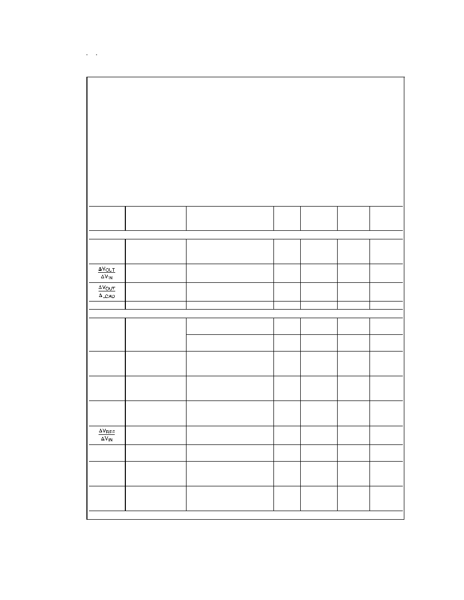
Electrical Characteristics -- LM1577-12, LM2577-12
Specifications with standard type face are for T
J
= 25∞C, and those in bold type face apply over full Operating Temperature
Range. Unless otherwise specified, V
IN
= 5V, and I
SWITCH
= 0.
LM1577-12
LM2577-12
Units
Symbol
Parameter
Conditions
Typical
Limit
Limit
(Limits)
(Notes 3, 4)
(Note 5)
SYSTEM PARAMETERS Circuit of
Figure 1 (Note 6)
V
OUT
Output Voltage
V
IN
= 5V to 10V
12.0
V
I
LOAD
= 100 mA to 800 mA
11.60/11.40
11.60/11.40
V(min)
(Note 3)
12.40/12.60
12.40/12.60
V(max)
Line Regulation
V
IN
= 3.5V to 10V
20
mV
I
LOAD
= 300 mA
50/100
50/100
mV(max)
Load Regulation
V
IN
= 5V
20
mV
I
LOAD
= 100 mA to 800 mA
50/100
50/100
mV(max)
Efficiency
V
IN
= 5V, I
LOAD
= 800 mA
80
%
DEVICE PARAMETERS
I
S
Input Supply Current
V
FEEDBACK
= 14V (Switch Off)
7.5
mA
10.0/14.0
10.0/14.0
mA(max)
I
SWITCH
= 2.0A
25
mA
V
COMP
= 2.0V (Max Duty Cycle)
50/85
50/85
mA(max)
V
UV
Input Supply
I
SWITCH
= 100 mA
2.90
V
Undervoltage Lockout
2.70/2.65
2.70/2.65
V(min)
3.10/3.15
3.10/3.15
V(max)
f
O
Oscillator Frequency
Measured at Switch Pin
52
kHz
I
SWITCH
= 100 mA
48/42
48/42
kHz(min)
56/62
56/62
kHz(max)
V
REF
Output Reference
Measured at Feedback Pin
V
Voltage
V
IN
= 3.5V to 40V
12
11.76/11.64
11.76/11.64
V(min)
V
COMP
= 1.0V
12.24/12.36
12.24/12.36
V(max)
Output Reference
V
IN
= 3.5V to 40V
7
mV
Voltage Line Regulator
R
FB
Feedback Pin Input
9.7
k
Resistance
G
M
Error Amp
I
COMP
= -30 µA to +30 µA
370
µmho
Transconductance
V
COMP
= 1.0V
225/145
225/145
µmho(min)
515/615
515/615
µmho(max)
A
VOL
Error Amp
V
COMP
= 1.1V to 1.9V
80
V/V
Voltage Gain
R
COMP
= 1.0 M
50/25
50/25
V/V(min)
(Note 7)
www.national.com
2

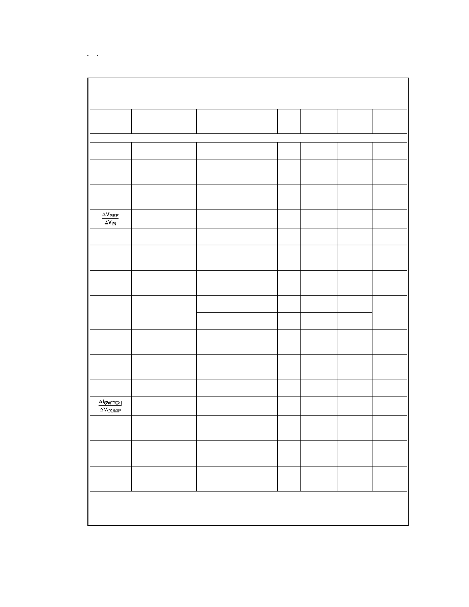
Electrical Characteristics -- LM1577-12, LM2577-12
(Continued)
Specifications with standard type face are for T
J
= 25∞C, and those in bold type face apply over full Operating Temperature
Range. Unless otherwise specified, V
IN
= 5V, and I
SWITCH
= 0.
LM1577-12
LM2577-12
Units
Symbol
Parameter
Conditions
Typical
Limit
Limit
(Limits)
(Notes 3, 4)
(Note 5)
DEVICE PARAMETERS
Error Amplifier
Upper Limit
2.4
V
Output Swing
V
FEEDBACK
= 10.0V
2.2/2.0
2.2/2.0
V(min)
Lower Limit
0.3
V
V
FEEDBACK
= 15.0V
0.40/0.55
0.40/0.55
V(max)
Error Amplifier
V
FEEDBACK
= 10.0V to 15.0V
±
200
µA
Output Current
V
COMP
= 1.0V
±
130/
±
90
±
130/
±
90
µA(min)
±
300/
±
400
±
300/
±
400
µA(max)
I
SS
Soft Start Current
V
FEEDBACK
= 10.0V
5.0
µA
V
COMP
= 0V
2.5/1.5
2.5/1.5
µA(min)
7.5/9.5
7.5/9.5
µA(max)
D
Maximum Duty Cycle
V
COMP
= 1.5V
95
%
I
SWITCH
= 100 mA
93/90
93/90
%(min)
Switch
Transconductance
12.5
A/V
I
L
Switch Leakage
V
SWITCH
= 65V
10
µA
Current
V
FEEDBACK
= 15V (Switch Off)
300/600
300/600
µA(max)
V
SAT
Switch Saturation
I
SWITCH
= 2.0A
0.5
V
Voltage
V
COMP
= 2.0V (Max Duty Cycle)
0.7/0.9
0.7/0.9
V(max)
NPN Switch
4.5
A
Current Limit
3.7/3.0
3.7/3.0
A(min)
5.3/6.0
5.3/6.0
A(max)
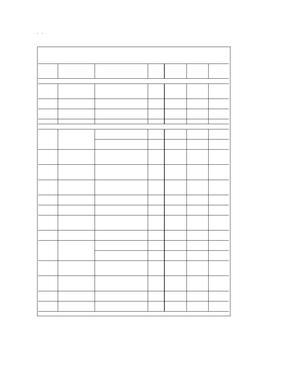
Electrical Characteristics -- LM1577-15, LM2577-15
Specifications with standard type face are for T
J
= 25∞C, and those in bold type face apply over full Operating Temperature
Range. Unless otherwise specified, V
IN
= 5V, and I
SWITCH
= 0.
LM1577-15
LM2577-15
Units
Symbol
Parameter
Conditions
Typical
Limit
Limit
(Limits)
(Notes 3, 4)
(Note 5)
SYSTEM PARAMETERS Circuit of
Figure 2 (Note 6)
V
OUT
Output Voltage
V
IN
= 5V to 12V
15.0
V
I
LOAD
= 100 mA to 600 mA
14.50/14.25
14.50/14.25
V(min)
(Note 3)
15.50/15.75
15.50/15.75
V(max)
Line Regulation
V
IN
= 3.5V to 12V
20
50/100
50/100
mV
I
LOAD
= 300 mA
mV(max)
Load Regulation
V
IN
= 5V
20
50/100
50/100
mV
I
LOAD
= 100 mA to 600 mA
mV(max)
Efficiency
V
IN
= 5V, I
LOAD
= 600 mA
80
%
DEVICE PARAMETERS
I
S
Input Supply Current
V
FEEDBACK
= 18.0V
7.5
mA
(Switch Off)
10.0/14.0
10.0/14.0
mA(max)
I
SWITCH
= 2.0A
25
mA
V
COMP
= 2.0V
50/85
50/85
mA(max)
(Max Duty Cycle)
V
UV
Input Supply
I
SWITCH
= 100 mA
2.90
V
www.national.com
3

Electrical Characteristics -- LM1577-15, LM2577-15
(Continued)
Specifications with standard type face are for T
J
= 25∞C, and those in bold type face apply over full Operating Temperature
Range. Unless otherwise specified, V
IN
= 5V, and I
SWITCH
= 0.
LM1577-15
LM2577-15
Units
Symbol
Parameter
Conditions
Typical
Limit
Limit
(Limits)
(Notes 3, 4)
(Note 5)
DEVICE PARAMETERS
Undervoltage
2.70/2.65
2.70/2.65
V(min)
Lockout
3.10/3.15
3.10/3.15
V(max)
f
O
Oscillator Frequency
Measured at Switch Pin
52
kHz
I
SWITCH
= 100 mA
48/42
48/42
kHz(min)
56/62
56/62
kHz(max)
V
REF
Output Reference
Measured at Feedback Pin
V
Voltage
V
IN
= 3.5V to 40V
15
14.70/14.55
14.70/14.55
V(min)
V
COMP
= 1.0V
15.30/15.45
15.30/15.45
V(max)
Output Reference
V
IN
= 3.5V to 40V
10
mV
Voltage Line Regulation
R
FB
Feedback Pin Input
12.2
k
Voltage Line Regulator
G
M
Error Amp
I
COMP
= -30 µA to +30 µA
300
µmho
Transconductance
V
COMP
= 1.0V
170/110
170/110
µmho(min)
420/500
420/500
µmho(max)
A
VOL
Error Amp
V
COMP
= 1.1V to 1.9V
65
V/V
Voltage Gain
R
COMP
= 1.0 M
40/20
40/20
V/V(min)
(Note 7)
Error Amplifier
Upper Limit
2.4
V
Output Swing
V
FEEDBACK
= 12.0V
2.2/2.0
2.2/2.0
V(min)
Lower Limit
0.3
V
V
FEEDBACK
= 18.0V
0.4/0.55
0.40/0.55
V(max)
Error Amp
V
FEEDBACK
= 12.0V to 18.0V
±
200
µA
Output Current
V
COMP
= 1.0V
±
130/
±
90
±
130/
±
90
µA(min)
±
300/
±
400
±
300/
±
400
µA(max)
I
SS
Soft Start Current
V
FEEDBACK
= 12.0V
5.0
µA
V
COMP
= 0V
2.5/1.5
2.5/1.5
µA(min)
7.5/9.5
7.5/9.5
µA(max)
D
Maximum Duty
V
COMP
= 1.5V
95
%
Cycle
I
SWITCH
= 100 mA
93/90
93/90
%(min)
Switch
Transconductance
12.5
A/V
I
L
Switch Leakage
V
SWITCH
= 65V
10
µA
Current
V
FEEDBACK
= 18.0V
300/600
300/600
µA(max)
(Switch Off)
V
SAT
Switch Saturation
I
SWITCH
= 2.0A
0.5
V
Voltage
V
COMP
= 2.0V
0.7/0.9
0.7/0.9
V(max)
(Max Duty Cycle)
NPN Switch
V
COMP
= 2.0V
4.3
A
Current Limit
3.7/3.0
3.7/3.0
A(min)
5.3/6.0
5.3/6.0
A(max)
www.national.com
4

Electrical Characteristics -- LM1577-ADJ, LM2577-ADJ
Specifications with standard type face are for T
J
= 25∞C, and those in bold type face apply over full Operating Temperature
Range. Unless otherwise specified, V
IN
= 5V, V
FEEDBACK
= V
REF
, and I
SWITCH
= 0.
LM1577-ADJ LM2577-ADJ
Units
Symbol
Parameter
Conditions
Typical
Limit
Limit
(Limits)
(Notes 3, 4)
(Note 5)
SYSTEM PARAMETERS Circuit of
Figure 3 (Note 6)
V
OUT
Output Voltage
V
IN
= 5V to 10V
12.0
V
I
LOAD
= 100 mA to 800 mA
11.60/11.40
11.60/11.40
V(min)
(Note 3)
12.40/12.60
12.40/12.60
V(max)
V
OUT
/
Line Regulation
V
IN
= 3.5V to 10V
20
mV
V
IN
I
LOAD
= 300 mA
50/100
50/100
mV(max)
V
OUT
/
Load Regulation
V
IN
= 5V
20
mV
I
LOAD
I
LOAD
= 100 mA to 800 mA
50/100
50/100
mV(max)
Efficiency
V
IN
= 5V, I
LOAD
= 800 mA
80
%
DEVICE PARAMETERS
I
S
Input Supply Current
V
FEEDBACK
= 1.5V (Switch Off)
7.5
mA
10.0/14.0
10.0/14.0
mA(max)
I
SWITCH
= 2.0A
25
mA
V
COMP
= 2.0V (Max Duty Cycle)
50/85
50/85
mA(max)
V
UV
Input Supply
I
SWITCH
= 100 mA
2.90
V
Undervoltage Lockout
2.70/2.65
2.70/2.65
V(min)
3.10/3.15
3.10/3.15
V(max)
f
O
Oscillator Frequency
Measured at Switch Pin
52
kHz
I
SWITCH
= 100 mA
48/42
48/42
kHz(min)
56/62
56/62
kHz(max)
V
REF
Reference
Measured at Feedback Pin
V
Voltage
V
IN
= 3.5V to 40V
1.230
1.214/1.206
1.214/1.206
V(min)
V
COMP
= 1.0V
1.246/1.254
1.246/1.254
V(max)
V
REF
/
Reference Voltage
V
IN
= 3.5V to 40V
0.5
mV
V
IN
Line Regulation
I
B
Error Amp
V
COMP
= 1.0V
100
nA
Input Bias Current
300/800
300/800
nA(max)
G
M
Error Amp
I
COMP
= -30 µA to +30 µA
3700
µmho
Transconductance
V
COMP
= 1.0V
2400/1600
2400/1600
µmho(min)
4800/5800
4800/5800
µmho(max)
A
VOL
Error Amp
V
COMP
= 1.1V to 1.9V
800
V/V
Voltage Gain
R
COMP
= 1.0 M
(Note 7)
500/250
500/250
V/V(min)
Error Amplifier
Upper Limit
2.4
V
Output Swing
V
FEEDBACK
= 1.0V
2.2/2.0
2.2/2.0
V(min)
Lower Limit
0.3
V
V
FEEDBACK
= 1.5V
0.40/0.55
0.40/0.55
V(max)
Error Amp
V
FEEDBACK
= 1.0V to 1.5V
±
200
µA
Output Current
V
COMP
= 1.0V
±
130/
±
90
±
130/
±
90
µA(min)
±
300/
±
400
±
300/
±
400
µA(max)
I
SS
Soft Start Current
V
FEEDBACK
= 1.0V
5.0
µA
V
COMP
= 0V
2.5/1.5
2.5/1.5
µA(min)
7.5/9.5
7.5/9.5
µA(max)
D
Maximum Duty Cycle
V
COMP
= 1.5V
95
%
I
SWITCH
= 100 mA
93/90
93/90
%(min)
I
SWITCH
/
Switch
12.5
A/V
V
COMP
Transconductance
www.national.com
5

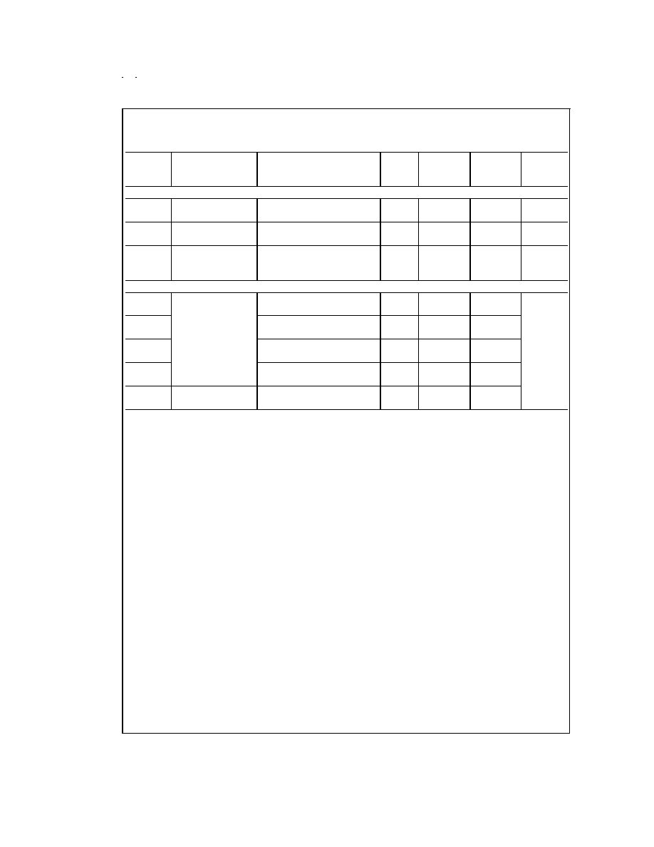
Electrical Characteristics -- LM1577-ADJ, LM2577-ADJ
(Continued)
Specifications with standard type face are for T
J
= 25∞C, and those in bold type face apply over full Operating Temperature
Range. Unless otherwise specified, V
IN
= 5V, V
FEEDBACK
= V
REF
, and I
SWITCH
= 0.
LM1577-ADJ LM2577-ADJ
Units
Symbol
Parameter
Conditions
Typical
Limit
Limit
(Limits)
(Notes 3, 4)
(Note 5)
DEVICE PARAMETERS
I
L
Switch Leakage
V
SWITCH
= 65V
10
µA
Current
V
FEEDBACK
= 1.5V (Switch Off)
300/600
300/600
µA(max)
V
SAT
Switch Saturation
I
SWITCH
= 2.0A
0.5
V
Voltage
V
COMP
= 2.0V (Max Duty Cycle)
0.7/0.9
0.7/0.9
V(max)
NPN Switch
V
COMP
= 2.0V
4.3
A
Current Limit
3.7/3.0
3.7/3.0
A(min)
5.3/6.0
5.3/6.0
A(max)
THERMAL PARAMETERS (All Versions)
JA
Thermal Resistance
K Package, Junction to Ambient
35
∞C/W
JC
K Package, Junction to Case
1.5
JA
T Package, Junction to Ambient
65
JC
T Package, Junction to Case
2
JA
N Package, Junction to
85
Ambient (Note 8)
JA
M Package, Junction
100
to Ambient (Note 8)
JA
S Package, Junction to
37
Ambient (Note 9)
Note 1: Absolute Maximum Ratings indicate limits beyond which damage to the device may occur. Operating ratings indicate conditions the device is intended to
be functional, but device parameter specifications may not be guaranteed under these conditions. For guaranteed specifications and test conditions, see the Electrical
Characteristics.
Note 2: Due to timing considerations of the LM1577/LM2577 current limit circuit, output current cannot be internally limited when the LM1577/LM2577 is used as a
step-up regulator. To prevent damage to the switch, its current must be externally limited to 6.0A. However, output current is internally limited when the LM1577/
LM2577 is used as a flyback or forward converter regulator in accordance to the Application Hints.
Note 3: All limits guaranteed at room temperature (standard type face) and at temperature extremes (boldface type). All limits are used to calculate Outgoing Quality
Level, and are 100% production tested.
Note 4: A military RETS electrical test specification is available on request. At the time of printing, the LM1577K-12/883, LM1577K-15/883, and LM1577K-ADJ/883
RETS specifications complied fully with the boldface limits in these columns. The LM1577K-12/883, LM1577K-15/883, and LM1577K-ADJ/883 may also be procured
to Standard Military Drawing specifications.
Note 5: All limits guaranteed at room temperature (standard type face) and at temperature extremes (boldface type). All room temperature limits are 100% produc-
tion tested. All limits at temperature extremes are guaranteed via correlation using standard Statistical Quality Control (SQC) methods.
Note 6: External components such as the diode, inductor, input and output capacitors can affect switching regulator performance. When the LM1577/LM2577 is used
as shown in the Test Circuit, system performance will be as specified by the system parameters.
Note 7: A 1.0 M
resistor is connected to the compensation pin (which is the error amplifier's output) to ensure accuracy in measuring A
VOL
. In actual applications,
this pin's load resistance should be
10 M
, resulting in A
VOL
that is typically twice the guaranteed minimum limit.
Note 8: Junction to ambient thermal resistance with approximately 1 square inch of pc board copper surrounding the leads. Additional copper area will lower thermal
resistance further. See thermal model in "Switchers Made Simple" software.
Note 9: If the TO-263 package is used, the thermal resistance can be reduced by increasing the PC board copper area thermally connected to the package. Using
0.5 square inches of copper area,
JA
is 50∞C/W; with 1 square inch of copper area,
JA
is 37∞C/W; and with 1.6 or more square inches of copper area,
JA
is 32∞C/W.
www.national.com
6

Typical Performance Characteristics
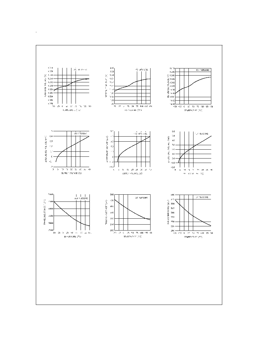
Reference Voltage
vs Temperature
DS011468-34
Reference Voltage
vs Temperature
DS011468-35
Reference Voltage
vs Temperature
DS011468-36
Reference Voltage
vs Supply Voltage
DS011468-37
Reference Voltage
vs Supply Voltage
DS011468-38
Reference Voltage
vs Supply Voltage
DS011468-39
Error Amp Transconductance
vs Temperature
DS011468-40
Error Amp Transconductance
vs Temperature
DS011468-41
Error Amp Transconductance
vs Temperature
DS011468-42
www.national.com
7

Typical Performance Characteristics
(Continued)
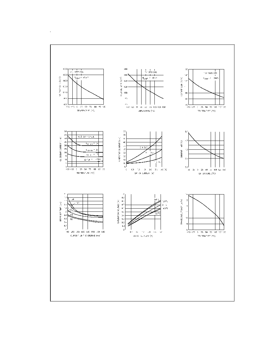
Error Amp Voltage
Gain vs Temperature
DS011468-43
Error Amp Voltage
Gain vs Temperature
DS011468-44
Error Amp Voltage
Gain vs Temperature
DS011468-45
Quiescent Current
vs Temperature
DS011468-46
Quiescent Current
vs Switch Current
DS011468-47
Current Limit
vs Temperature
DS011468-48
Current Limit Response
Time vs Overdrive
DS011468-49
Switch Saturation Voltage
vs Switch Current
DS011468-50
Switch Transconductance
vs Temperature
DS011468-51
www.national.com
8

Typical Performance Characteristics
(Continued)
Connection Diagrams
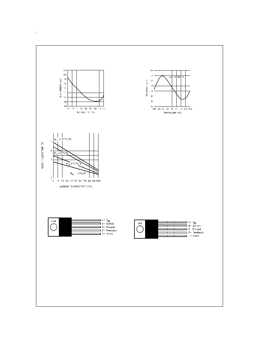
Feedback Pin Bias
Current vs Temperature
DS011468-52
Oscillator Frequency
vs Temperature
DS011468-53
Maximum Power Dissipation
(TO-263) (Note 9)
DS011468-31
Straight Leads
5-Lead TO-220 (T)
DS011468-4
Top View
Order Number LM2577T-12, LM2577T-15,
or LM2577T-ADJ
See NS Package Number T05A
Bent, Staggered Leads
5-Lead TO-220 (T)
DS011468-5
Top View
Order Number LM2577T-12 Flow LB03, LM2577T-15
Flow LB03, or LM2577T-ADJ Flow LB03
See NS Package Number T05D
www.national.com
9

Connection Diagrams
(Continued)
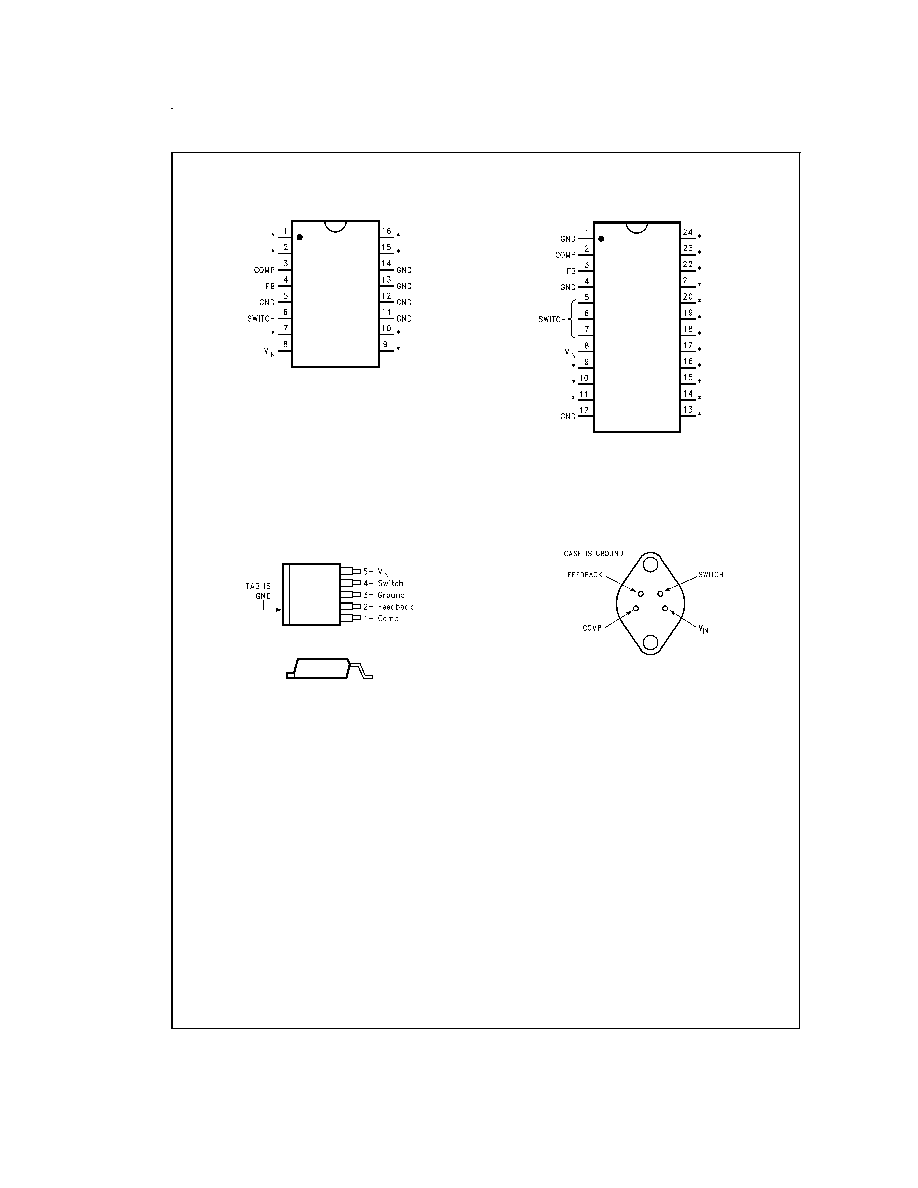
16-Lead DIP (N)
DS011468-6
*
No internal Connection
Top View
Order Number LM2577N-12, LM2577N-15,
or LM2577N-ADJ
See NS Package Number N16A
24-Lead Surface Mount (M)
DS011468-7
*
No internal Connection
Top View
Order Number LM2577M-12, LM2577M-15,
or LM2577M-ADJ
See NS Package Number M24B
TO-263 (S)
5-Lead Surface-Mount Package
DS011468-32
Top View
DS011468-33
Side View
Order Number LM2577S-12, LM2577S-15,
or LM2577S-ADJ
See NS Package Number TS5B
4-Lead TO-3 (K)
DS011468-8
Bottom View
Order Number LM1577K-12/883, LM1577K-15/883,
or LM1577K-ADJ/883
See NS Package Number K04A
www.national.com
10

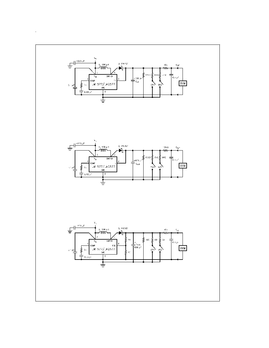
LM1577-12, LM2577-12 Test Circuit
LM1577-15, LM2577-15 Test Circuit
LM1577-ADJ, LM2577-ADJ Test Circuit
DS011468-30
L = 415-0930 (AIE)
D = any manufacturer
C
OUT
= Sprague Type 673D
Electrolytic 680 µF, 20V
Note: Pin numbers shown are for TO-220 (T) package
FIGURE 1. Circuit Used to Specify System Parameters for 12V Versions
DS011468-26
L = 415-0930 (AIE)
D = any manufacturer
C
OUT
= Sprague Type 673D
Electrolytic 680 µF, 20V
Note: Pin numbers shown are for TO-220 (T) package
FIGURE 2. Circuit Used to Specify System Parameters for 15V Versions
DS011468-9
L = 415-0930 (AIE)
D = any manufacturer
C
OUT
= Sprague Type 673D
Electrolytic 680 µF, 20V
R1 = 48.7k in series with 511
(1%)
R2 = 5.62k (1%)
Note: Pin numbers shown are for TO-220 (T) package
FIGURE 3. Circuit Used to Specify System Parameters for ADJ Versions
www.national.com
11

Application Hints
DS011468-10
Note: Pin numbers shown are for TO-220 (T) package
*
Resistors are internal to LM1577/LM2577 for 12V and 15V versions.
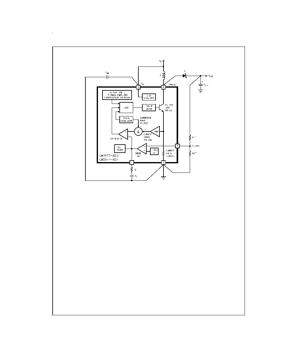
FIGURE 4. LM1577/LM2577 Block Diagram and Boost Regulator Application
www.national.com
12

Application Hints
(Continued)
STEP-UP (BOOST) REGULATOR
Figure 4 shows the LM1577-ADJ/LM2577-ADJ used as a
Step-Up Regulator. This is a switching regulator used for
producing an output voltage greater than the input supply
voltage.
The
LM1577-12/LM2577-12
and
LM1577-15/
LM2577-15 can also be used for step-up regulators with 12V
or 15V outputs (respectively), by tying the feedback pin di-
rectly to the regulator output.
A basic explanation of how it works is as follows. The
LM1577/LM2577 turns its output switch on and off at a fre-
quency of 52 kHz, and this creates energy in the inductor (L).
When the NPN switch turns on, the inductor current charges
up at a rate of V
IN
/L, storing current in the inductor. When the
switch turns off, the lower end of the inductor flies above V
IN
,
discharging its current through diode (D) into the output ca-
pacitor (C
OUT
) at a rate of (V
OUT
- V
IN
)/L. Thus, energy
stored in the inductor during the switch on time is transferred
to the output during the switch off time. The output voltage is
controlled by the amount of energy transferred which, in turn,
is controlled by modulating the peak inductor current. This is
done by feeding back a portion of the output voltage to the
error amp, which amplifies the difference between the feed-
back voltage and a 1.230V reference. The error amp output
voltage is compared to a voltage proportional to the switch
current (i.e., inductor current during the switch on time).
The comparator terminates the switch on time when the two
voltages are equal, thereby controlling the peak switch cur-
rent to maintain a constant output voltage.
Voltage and current waveforms for this circuit are shown in
Figure 5, and formulas for calculating them are given in Fig-
ure 6.
STEP-UP REGULATOR DESIGN PROCEDURE
The following design procedure can be used to select the ap-
propriate external components for the circuit in
Figure 4,
based on these system requirements.
Given:
V
IN (min)
= Minimum input supply voltage
V
OUT
= Regulated output voltage
I
LOAD(max)
= Maximum output load current
Before proceeding any further, determine if the LM1577/
LM2577 can provide these values of V
OUT
and I
LOAD(max)
when operating with the minimum value of V
IN
. The upper
limits for V
OUT
and I
LOAD(max)
are given by the following
equations.
V
OUT
60V
and
V
OUT
10 x V
IN(min)
These limits must be greater than or equal to the values
specified in this application.
1. Inductor Selection (L)
A.
Voltage Options:
1. For 12V or 15V output
DS011468-11
FIGURE 5. Step-Up Regulator Waveforms
Duty Cycle
D
Average
Inductor
Current
I
IND(AVE)
Inductor
Current
Ripple
I
IND
Peak
Inductor
Current
I
IND(PK)
Peak Switch
Current
I
SW(PK)
Switch
Voltage
When Off
V
SW(OFF)
V
OUT
+ V
F
Diode
Reverse
Voltage
V
R
V
OUT
- V
SAT
Average
Diode
Current
I
D(AVE)
I
LOAD
Peak Diode
Current
I
D(PK)
Power
Dissipation
of
LM1577/2577
P
D
V
F
= Forward Biased Diode Voltage
I
LOAD
= Output Load Current
FIGURE 6. Step-Up Regulator Formulas
www.national.com
13

Application Hints
(Continued)
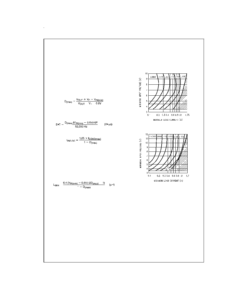
From
Figure 7 (for 12V output) or Figure 8 (for 15V
output), identify inductor code for region indicated by
V
IN (min)
and I
LOAD (max)
. The shaded region indicates
conditions for which the LM1577/LM2577 output switch
would be operating beyond its switch current rating. The
minimum operating voltage for the LM1577/LM2577 is
3.5V.
From here,
proceed to step C.
2. For Adjustable version
Preliminary calculations:
The inductor selection is based on the calculation of the
following three parameters:
D
(max)
, the maximum switch duty cycle (0
D
0.9):
where V
F
= 0.5V for Schottky diodes and 0.8V for fast recov-
ery diodes (typically);
E
∑T, the product of volts x time that charges the inductor:
I
IND,DC
, the average inductor current under full load;
B.
Identify Inductor Value:
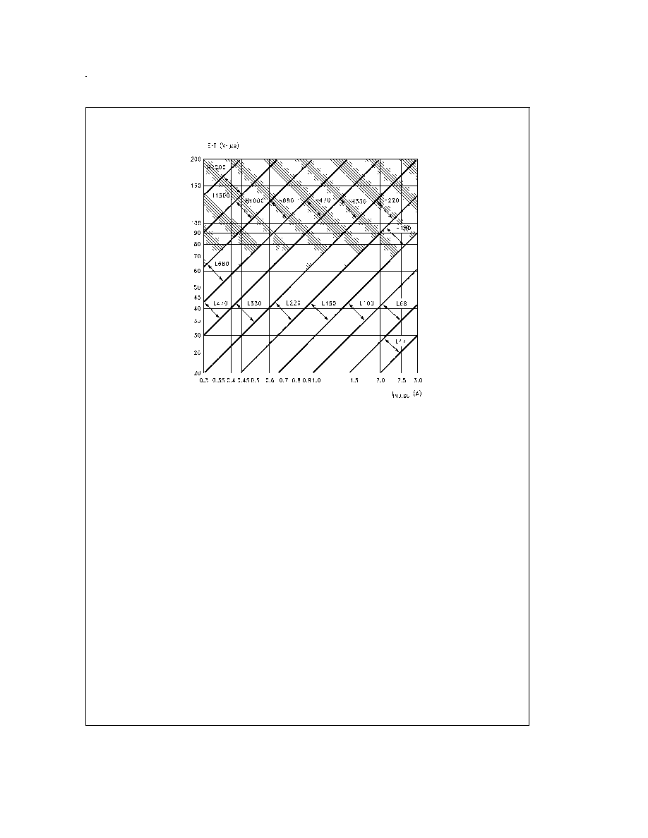
1. From
Figure 9, identify the inductor code for the re-
gion indicated by the intersection of E
∑T and I
IND,DC
.
This code gives the inductor value in microhenries. The
L or H prefix signifies whether the inductor is rated for a
maximum E
∑T of 90 V∑µs (L) or 250 V∑µs (H).
2. If D
<
0.85, go on to step C. If D
0.85, then calcu-
late the minimum inductance needed to ensure the
switching regulator's stability:
If L
MIN
is smaller than the inductor value found in step B1, go
on to step C. Otherwise, the inductor value found in step B1
is too low; an appropriate inductor code should be obtained
from the graph as follows:
1. Find the lowest value inductor that is greater than L
MIN
.
2. Find where E
∑T intersects this inductor value to determine
if it has an L or H prefix. If E
∑T intersects both the L and H re-
gions, select the inductor with an H prefix.
DS011468-27
FIGURE 7. LM2577-12 Inductor Selection Guide
DS011468-28
FIGURE 8. LM2577-15 Inductor Selection Guide
www.national.com
14

Application Hints
(Continued)
C.
Select an inductor from the table of Figure 10 which
cross-references the inductor codes to the part numbers
of three different manufacturers. Complete specifica-
tions for these inductors are available from the respec-
tive manufacturers. The inductors listed in this table
have the following characteristics:
AIE: ferrite, pot-core inductors; Benefits of this type are
low electro-magnetic interference (EMI), small physical
size, and very low power dissipation (core loss). Be
careful not to operate these inductors too far beyond
their maximum ratings for E
∑T and peak current, as this
will saturate the core.
Pulse: powdered iron, toroid core inductors; Benefits are
low EMI and ability to withstand E
∑T and peak current
above rated value better than ferrite cores.
Renco: ferrite, bobbin-core inductors; Benefits are low
cost and best ability to withstand E
∑T and peak current
above rated value. Be aware that these inductors gener-
ate more EMI than the other types, and this may inter-
fere with signals sensitive to noise.
DS011468-12
Note: These charts assume that the inductor ripple current inductor is approximately 20% to 30% of the average inductor current (when the regulator is under
full load). Greater ripple current causes higher peak switch currents and greater output ripple voltage; lower ripple current is achieved with larger-value
inductors. The factor of 20 to 30% is chosen as a convenient balance between the two extremes.
FIGURE 9. LM1577-ADJ/LM2577-ADJ Inductor Selection Graph
www.national.com
15

Application Hints
(Continued)
2. Compensation Network (R
C
, C
C
) and Output Capacitor
(C
OUT
) Selection
R
C
and C
C
form a pole-zero compensation network that sta-
bilizes the regulator. The values of R
C
and C
C
are mainly de-
pendant on the regulator voltage gain, I
LOAD(max)
, L and
C
OUT
. The following procedure calculates values for R
C
, C
C
,
and C
OUT
that ensure regulator stability. Be aware that this
procedure doesn't necessarily result in R
C
and C
C
that pro-
vide optimum compensation. In order to guarantee optimum
compensation, one of the standard procedures for testing
loop stability must be used, such as measuring V
OUT
tran-
sient response when pulsing I
LOAD
(see
Figure 15).
A.
First, calculate the maximum value for R
C
.
Select a resistor less than or equal to this value, and it
should also be no greater than 3 k
.
B.
Calculate the minimum value for C
OUT
using the following
two equations.
The larger of these two values is the minimum value that en-
sures stability.
C.
Calculate the minimum value of C
C
.
The compensation capacitor is also part of the soft start cir-
cuitry. When power to the regulator is turned on, the switch
duty cycle is allowed to rise at a rate controlled by this ca-
pacitor (with no control on the duty cycle, it would immedi-
ately rise to 90%, drawing huge currents from the input
power supply). In order to operate properly, the soft start cir-
cuit requires C
C
0.22 µF.
The value of the output filter capacitor is normally large
enough to require the use of aluminum electrolytic capaci-
tors.
Figure 11 lists several different types that are recom-
mended for switching regulators, and the following param-
eters are used to select the proper capacitor.
Working Voltage (WVDC): Choose a capacitor with a work-
ing voltage at least 20% higher than the regulator output volt-
age.
Ripple Current: This is the maximum RMS value of current
that charges the capacitor during each switching cycle. For
step-up and flyback regulators, the formula for ripple current
is
Choose a capacitor that is rated at least 50% higher than this
value at 52 kHz.
Equivalent Series Resistance (ESR) : This is the primary
cause of output ripple voltage, and it also affects the values
of R
C
and C
C
needed to stabilize the regulator. As a result,
the preceding calculations for C
C
and R
C
are only valid if
ESR doesn't exceed the maximum value specified by the fol-
lowing equations.
Select a capacitor with ESR, at 52 kHz, that is less than or
equal to the lower value calculated. Most electrolytic capaci-
tors specify ESR at 120 Hz which is 15% to 30% higher than
at 52 kHz. Also, be aware that ESR increases by a factor of
2 when operating at -20∞C.
In general, low values of ESR are achieved by using large
value capacitors (C
470 µF), and capacitors with high
WVDC, or by paralleling smaller-value capacitors.
Inductor
Manufacturer's Part Number
Code
Schott
Pulse
Renco
L47
67126980
PE - 53112
RL2442
L68
67126990
PE - 92114
RL2443
L100
67127000
PE - 92108
RL2444
L150
67127010
PE - 53113
RL1954
L220
67127020
PE - 52626
RL1953
L330
67127030
PE - 52627
RL1952
L470
67127040
PE - 53114
RL1951
L680
67127050
PE - 52629
RL1950
H150
67127060
PE - 53115
RL2445
H220
67127070
PE - 53116
RL2446
H330
67127080
PE - 53117
RL2447
H470
67127090
PE - 53118
RL1961
H680
67127100
PE - 53119
RL1960
H1000
67127110
PE - 53120
RL1959
H1500
67127120
PE - 53121
RL1958
H2200
67127130
PE - 53122
RL2448
Schott Corp., (612) 475-1173
1000 Parkers Lake Rd., Wayzata, MN 55391
Pulse Engineering, (619) 268-2400
P.O. Box 12235, San Diego, CA 92112
Renco Electronics Inc., (516) 586-5566
60 Jeffryn Blvd. East, Deer Park, NY 11729
FIGURE 10. Table of Standardized Inductors and
Manufacturer's Part Numbers
www.national.com
16

Application Hints
(Continued)
3. Output Voltage Selection (R1 and R2)
This section is for applications using the LM1577-ADJ/
LM2577-ADJ. Skip this section if the LM1577-12/LM2577-12
or LM1577-15/LM2577-15 is being used.
With the LM1577-ADJ/LM2577-ADJ, the output voltage is
given by
V
OUT
= 1.23V (1 + R1/R2)
Resistors R1 and R2 divide the output down so it can be
compared
with
the
LM1577-ADJ/LM2577-ADJ
internal
1.23V reference. For a given desired output voltage V
OUT
,
select R1 and R2 so that
4. Input Capacitor Selection (C
IN
)
The switching action in the step-up regulator causes a trian-
gular ripple current to be drawn from the supply source. This
in turn causes noise to appear on the supply voltage. For
proper operation of the LM1577, the input voltage should be
decoupled. Bypassing the Input Voltage pin directly to
ground with a good quality, low ESR, 0.1 µF capacitor (leads
as short as possible) is normally sufficient.
If the LM1577 is located far from the supply source filter ca-
pacitors, an additional large electrolytic capacitor (e.g.
47 µF) is often required.
5. Diode Selection (D)
The switching diode used in the boost regulator must with-
stand a reverse voltage equal to the circuit output voltage,
and must conduct the peak output current of the LM2577. A
suitable diode must have a minimum reverse breakdown
voltage greater than the circuit output voltage, and should be
rated for average and peak current greater than I
LOAD(max)
and I
D(PK)
. Schottky barrier diodes are often favored for use
in switching regulators. Their low forward voltage drop allows
higher regulator efficiency than if a (less expensive) fast re-
covery diode was used. See
Figure 12 for recommended
part numbers and voltage ratings of 1A and 3A diodes.
BOOST REGULATOR CIRCUIT EXAMPLE
By adding a few external components (as shown in
Figure
13), the LM2577 can be used to produce a regulated output
voltage that is greater than the applied input voltage. Typical
performance of this regulator is shown in
Figure 14 and Fig-
ure 15. The switching waveforms observed during the opera-
tion of this circuit are shown in
Figure 16.
Cornell Dublier -- Types 239, 250, 251, UFT,
300, or 350
P.O. Box 128, Pickens, SC 29671
(803) 878-6311
Nichicon -- Types PF, PX, or PZ
927 East Parkway,
Schaumburg, IL 60173
(708) 843-7500
Sprague -- Types 672D, 673D, or 674D
Box 1, Sprague Road,
Lansing, NC 28643
(919) 384-2551
United Chemi-Con -- Types LX, SXF, or SXJ
9801 West Higgins Road,
Rosemont, IL 60018
(708) 696-2000
FIGURE 11. Aluminum Electrolytic Capacitors
Recommended for Switching Regulators
V
OUT
Schottky
Fast Recovery
(max)
1A
3A
1A
3A
20V
1N5817
1N5820
MBR120P
MBR320P
1N5818
1N5821
30V
MBR130P
MBR330P
11DQ03
31DQ03
1N5819
1N5822
40V
MBR140P
MBR340P
11DQ04
31DQ04
MBR150
MBR350
1N4933
50V
11DQ05
31DQ05
MUR105
1N4934
MR851
100V
HER102
30DL1
MUR110
MR831
10DL1
HER302
FIGURE 12. Diode Selection Chart
www.national.com
17

Application Hints
(Continued)
DS011468-13
Note: Pin numbers shown are for TO-220 (T) package.
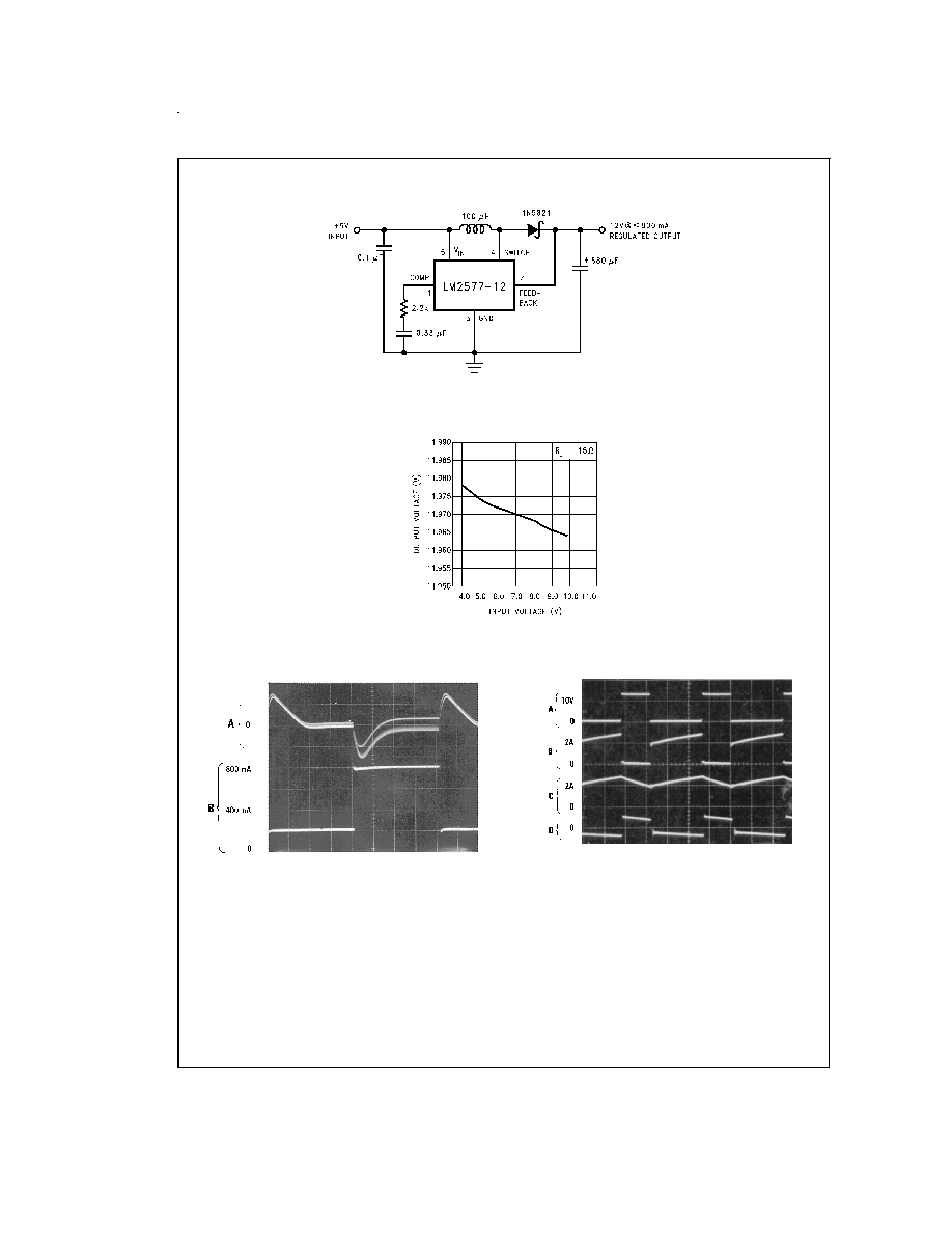
FIGURE 13. Step-up Regulator Delivers 12V from a 5V Input
DS011468-14
FIGURE 14. Line Regulation (Typical) of Step-Up Regulator of
Figure 13
DS011468-15
A: Output Voltage Change, 100 mV/div. (AC-coupled)
B: Load current, 0.2 A/div
Horizontal: 5 ms/div
FIGURE 15. Load Transient Response of Step-Up
Regulator of
Figure 13
DS011468-16
A: Switch pin voltage, 10 V/div
B: Switch pin current, 2 A/div
C: Inductor current, 2 A/div
D: Output ripple voltage, 100 mV/div (AC-coupled)
Horizontal: 5 µs/div
FIGURE 16. Switching Waveforms of Step-Up
Regulator of
Figure 13
www.national.com
18

Application Hints
(Continued)
FLYBACK REGULATOR
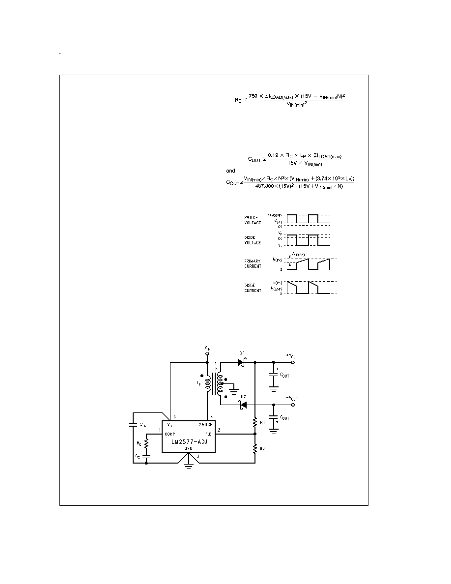
A Flyback regulator can produce single or multiple output
voltages that are lower or greater than the input supply volt-
age.
Figure 18 shows the LM1577/LM2577 used as a fly-
back regulator with positive and negative regulated outputs.
Its operation is similar to a step-up regulator, except the out-
put switch contols the primary current of a flyback trans-
former. Note that the primary and secondary windings are
out of phase, so no current flows through secondary when
current flows through the primary. This allows the primary to
charge up the transformer core when the switch is on. When
the switch turns off, the core discharges by sending current
through the secondary, and this produces voltage at the out-
puts. The output voltages are controlled by adjusting the
peak primary current, as described in the step-up regulator
section.
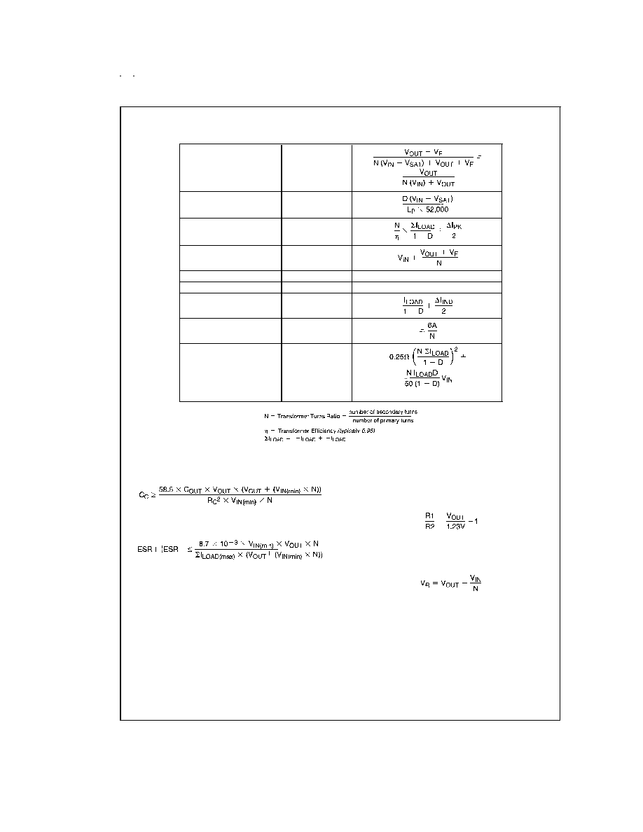
Voltage and current waveforms for this circuit are shown in
Figure 17, and formulas for calculating them are given in Fig-
ure 19.
FLYBACK REGULATOR DESIGN PROCEDURE
1. Transformer Selection
A family of standardized flyback transformers is available for
creating flyback regulators that produce dual output volt-
ages, from
±
10V to
±
15V, as shown in
Figure 18. Figure
20lists these transformers with the input voltage, output volt-
ages and maximum load current they are designed for.
2. Compensation Network (C
C
, R
C
) and
Output Capacitor (C
OUT
) Selection
As explained in the Step-Up Regulator Design Procedure,
C
C
, R
C
and C
OUT
must be selected as a group. The following
procedure is for a dual output flyback regulator with equal
turns ratios for each secondary (i.e., both output voltages
have the same magnitude). The equations can be used for a
single output regulator by changing
I
LOAD(max)
to I
LOAD(max)
in the following equations.
A. First, calculate the maximum value for R
C
.
Where
I
LOAD(max)
is the sum of the load current (magni-
tude) required from both outputs. Select a resistor less than
or equal to this value, and no greater than 3 k
.
B. Calculate the minimum value for
C
OUT
(sum of C
OUT
at both outputs) using the following two equations.
The larger of these two values must be used to ensure regu-
lator stability.
DS011468-17
FIGURE 17. Flyback Regulator Waveforms
DS011468-18
T1 = Pulse Engineering, PE-65300
D1, D2 = 1N5821
FIGURE 18. LM1577-ADJ/LM2577-ADJ Flyback Regulator with
±
Outputs
www.national.com
19

Application Hints
(Continued)
C.
Calculate the minimum value of C
C
D.
Calculate the maximum ESR of the +V
OUT
and -V
OUT
output capacitors in parallel.
This formula can also be used to calculate the maximum
ESR of a single output regulator.
At this point, refer to this same section in the Step-Up Regu-
lator Design Procedurefor more information regarding the
selection of C
OUT
.
3. Output Voltage Selection
This section is for applications using the LM1577-ADJ/
LM2577-ADJ. Skip this section if the LM1577-12/LM2577-12
or LM1577-15/LM2577-15 is being used.
With the LM1577-ADJ/LM2577-ADJ, the output voltage is
given by
V
OUT
= 1.23V (1 + R1/R2)
Resistors R1 and R2 divide the output voltage down so it can
be compared with the LM1577-ADJ/LM2577-ADJ internal
1.23V reference. For a desired output voltage V
OUT
, select
R1 and R2 so that
4. Diode Selection
The switching diode in a flyback converter must withstand
the reverse voltage specified by the following equation.
A suitable diode must have a reverse voltage rating greater
than this. In addition it must be rated for more than the aver-
age and peak diode currents listed in
Figure 19.
5. Input Capacitor Selection
The primary of a flyback transformer draws discontinuous
pulses of current from the input supply. As a result, a flyback
regulator generates more noise at the input supply than a
step-up regulator, and this requires a larger bypass capacitor
to decouple the LM1577/LM2577 V
IN
pin from this noise. For
most applications, a low ESR, 1.0 µF cap will be sufficient, if
it is connected very close to the V
IN
and Ground pins.
Duty Cycle
D
Primary Current Variation
I
P
Peak Primary Current
I
P(PK)
Switch Voltage when Off
V
SW(OFF)
Diode Reverse Voltage
V
R
V
OUT
+
N (V
IN
-
V
SAT
)
Average Diode Current
I
D(AVE)
I
LOAD
Peak Diode Current
I
D(PK)
Short Circuit Diode Current
Power Dissipation of
LM1577/LM2577
P
D
DS011468-78
FIGURE 19. Flyback Regulator Formulas
www.national.com
20

Application Hints
(Continued)
Transformer
Input
Dual
Maxi-
mum
Type
Voltage
Output
Output
Voltage
Current
L
P
= 100 µH
5V
±
10V
325 mA
1
N = 1
5V
±
12V
275 mA
5V
±
15V
225 mA
10V
±
10V
700 mA
10V
±
12V
575 mA
2
L
P
= 200 µH
10V
±
15V
500 mA
N = 0.5
12V
±
10V
800 mA
12V
±
12V
700 mA
12V
±
15V
575 mA
3
L
P
= 250 µH
15V
±
10V
900 mA
N = 0.5
15V
±
12V
825 mA
15V
±
15V
700 mA
In addition to this bypass cap, a larger capacitor (
47 µF)
should be used where the flyback transformer connects to
the input supply. This will attenuate noise which may inter-
fere with other circuits connected to the same input supply
voltage.
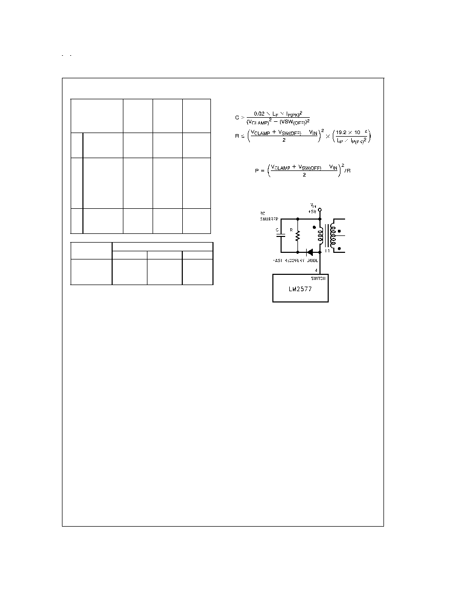
6. Snubber Circuit
A "snubber" circuit is required when operating from input
voltages greater than 10V, or when using a transformer with
L
P
200 µH. This circuit clamps a voltage spike from the
transformer primary that occurs immediately after the output
switch turns off. Without it, the switch voltage may exceed
the 65V maximum rating. As shown in
Figure 21, the snub-
ber consists of a fast recovery diode, and a parallel RC. The
RC values are selected for switch clamp voltage (V
CLAMP
)
that is 5V to 10V greater than V
SW(OFF)
. Use the following
equations to calculate R and C;
Power dissipation (and power rating) of the resistor is;
The fast recovery diode must have a reverse voltage rating
greater than V
CLAMP
.
FLYBACK REGULATOR CIRCUIT EXAMPLE
The circuit of
Figure 22 produces
±
15V (at 225 mA each)
from a single 5V input. The output regulation of this circuit is
shown in
Figure 23 and Figure 25, while the load transient
response is shown in
Figure 24 and Figure 26. Switching
waveforms seen in this circuit are shown in
Figure 27.
Transformer
Manufacturers' Part Numbers
Type
AIE
Pulse
Renco
1
326-0637
PE-65300
RL-2580
2
330-0202
PE-65301
RL-2581
3
330-0203
PE-65302
RL-2582
FIGURE 20. Flyback Transformer Selection Guide
DS011468-19
FIGURE 21. Snubber Circuit
www.national.com
21

Application Hints
(Continued)
DS011468-20
T1 = Pulse Engineering, PE-65300
D1, D2 = 1N5821
FIGURE 22. Flyback Regulator Easily Provides Dual Outputs
DS011468-21
FIGURE 23. Line Regulation (Typical) of Flyback
Regulator of
Figure 22, +15V Output
DS011468-23
A: Output Voltage Change, 100 mV/div
B: Output Current, 100 mA/div
Horizontal: 10 ms/div
FIGURE 24. Load Transient Response of Flyback
Regulator of
Figure 22, +15V Output
DS011468-22
FIGURE 25. Line Regulation (Typical) of Flyback
Regulator of
Figure 22, -15V Output
DS011468-24
A: Output Voltage Change, 100 mV/div
B: Output Current, 100 mA/div
Horizontal: 10 ms/div
FIGURE 26. Load Transient Response of Flyback
Regulator of
Figure 22, -15V Output
www.national.com
22

Application Hints
(Continued)
DS011468-25
A: Switch pin voltage, 20 V/div
B: Primary current, 2 A/div
C: +15V Secondary current, 1 A/div
D: +15V Output ripple voltage, 100 mV/div
Horizontal: 5 µs/div
FIGURE 27. Switching Waveforms of Flyback Regulator of
Figure 22, Each Output Loaded with 60
www.national.com
23

Physical Dimensions
inches (millimeters) unless otherwise noted
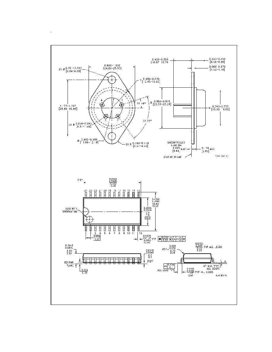
TO-3 Metal Can Package (K)
Order Number LM1577K-12/883, LM1577K-15/883, or LM1577K-ADJ/883
NS Package Number K04A
0.300 Wide SO Package (M)
Order Number LM2577M-12, LM2577M-15 or LM2577M-ADJ
NS Package Number M24B
www.national.com
24

Physical Dimensions
inches (millimeters) unless otherwise noted (Continued)
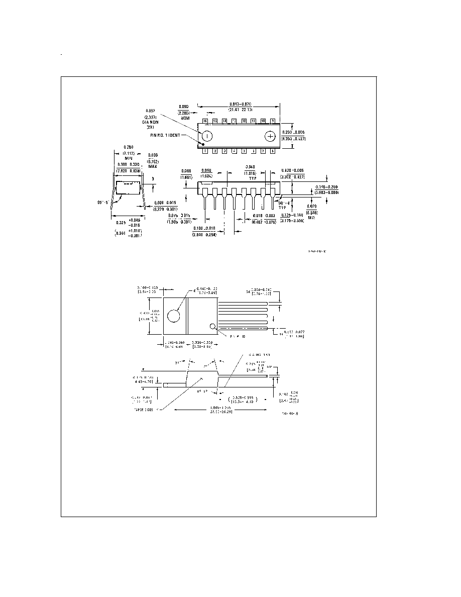
Molded Dual-In-Line Package (N)
Order Number LM2577N-12, LM2577N-15, or LM2577N-ADJ
NS Package Number N16A
TO-220, Straight Leads (T)
Order Number LM2577T-12, LM2577T-15, or LM2577T-ADJ
NS Package Number TO5A
www.national.com
25

Physical Dimensions
inches (millimeters) unless otherwise noted (Continued)
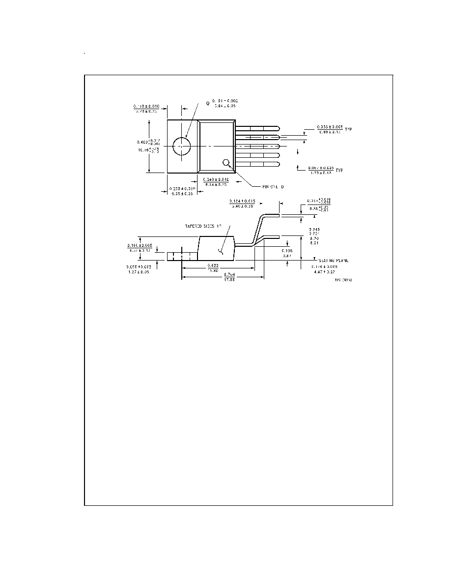
TO-220, Bent Staggered Leads (T)
Order Number LM2577T-12 Flow LB03, LM2577T-15 Flow LB03, or LM2577T-ADJ Flow LB03
NS Package Number T05D
www.national.com
26

Physical Dimensions
inches (millimeters) unless otherwise noted (Continued)
LIFE SUPPORT POLICY
NATIONAL'S PRODUCTS ARE NOT AUTHORIZED FOR USE AS CRITICAL COMPONENTS IN LIFE SUPPORT
DEVICES OR SYSTEMS WITHOUT THE EXPRESS WRITTEN APPROVAL OF THE PRESIDENT AND GENERAL
COUNSEL OF NATIONAL SEMICONDUCTOR CORPORATION. As used herein:
1. Life support devices or systems are devices or
systems which, (a) are intended for surgical implant
into the body, or (b) support or sustain life, and
whose failure to perform when properly used in
accordance with instructions for use provided in the
labeling, can be reasonably expected to result in a
significant injury to the user.
2. A critical component is any component of a life
support device or system whose failure to perform
can be reasonably expected to cause the failure of
the life support device or system, or to affect its
safety or effectiveness.
National Semiconductor
Corporation
Americas
Tel: 1-800-272-9959
Fax: 1-800-737-7018
Email: support@nsc.com
National Semiconductor
Europe
Fax: +49 (0) 1 80-530 85 86
Email: europe.support@nsc.com
Deutsch Tel: +49 (0) 1 80-530 85 85
English
Tel: +49 (0) 1 80-532 78 32
FranÁais Tel: +49 (0) 1 80-532 93 58
Italiano
Tel: +49 (0) 1 80-534 16 80
National Semiconductor
Asia Pacific Customer
Response Group
Tel: 65-2544466
Fax: 65-2504466
Email: sea.support@nsc.com
National Semiconductor
Japan Ltd.
Tel: 81-3-5639-7560
Fax: 81-3-5639-7507
www.national.com
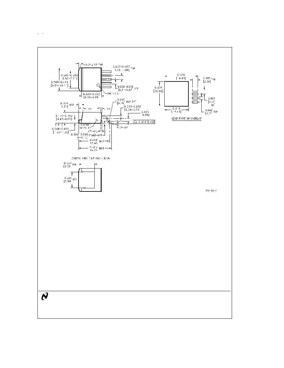
5-Lead TO-263 (S)
Order Number LM2577S-12, LM2577S-15 or LM2577S-ADJ
NS Package Number TS5B
LM1577/LM2577
Series
SIMPLE
SWITCHER
Step-Up
V
oltage
Regulator
National does not assume any responsibility for use of any circuitry described, no circuit patent licenses are implied and National reserves the right at any time without notice to change said circuitry and specifications.

