LM2587
SIMPLE SWITCHER
ģ
5A Flyback Regulator
General Description
The LM2587 series of regulators are monolithic integrated
circuits specifically designed for flyback, step-up (boost), and
forward converter applications. The device is available in 4
different output voltage versions: 3.3V, 5.0V, 12V, and adjust-
able.
Requiring a minimum number of external components, these
regulators are cost effective, and simple to use. Included in
the datasheet are typical circuits of boost and flyback regula-
tors. Also listed are selector guides for diodes and capacitors
and a family of standard inductors and flyback transformers
designed to work with these switching regulators.
The power switch is a 5.0A NPN device that can stand-off
65V. Protecting the power switch are current and thermal
limiting circuits, and an undervoltage lockout circuit. This IC
contains a 100 kHz fixed-frequency internal oscillator that
permits the use of small magnetics. Other features include
soft start mode to reduce in-rush current during start up, cur-
rent mode control for improved rejection of input voltage and
output load transients and cycle-by-cycle current limiting. An
output voltage tolerance of
Ī
4%, within specified input volt-
ages and output load conditions, is guaranteed for the power
supply system.
Features
n
Requires few external components
n
Family of standard inductors and transformers
n
NPN output switches 5.0A, can stand off 65V
n
Wide input voltage range: 4V to 40V
n
Current-mode operation for improved transient
response, line regulation, and current limit
n
100 kHz switching frequency
n
Internal soft-start function reduces in-rush current during
start-up
n
Output transistor protected by current limit, under
voltage lockout, and thermal shutdown
n
System Output Voltage Tolerance of
Ī
4% max over line
and load conditions
Typical Applications
n
Flyback regulator
n
Multiple-output regulator
n
Simple boost regulator
n
Forward converter
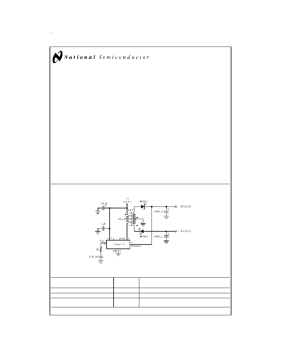
Flyback Regulator
Ordering Information
Package Type
NSC Package
Order Number
Drawing
5-Lead TO-220 Bent, Staggered Leads
T05D
LM2587T-3.3, LM2587T-5.0, LM2587T-12, LM2587T-ADJ
5-Lead TO-263
TS5B
LM2587S-3.3, LM2587S-5.0, LM2587S-12, LM2587S-ADJ
5-Lead TO-263 Tape and Reel
TS5B
LM2587SX-3.3, LM2587SX-5.0, LM2587SX-12,
LM2587SX-ADJ
SIMPLE SWITCHER
ģ
and
Switchers Made Simple
ģ
are registered trademarks of National Semiconductor Corporation.
DS012316-1
April 1998
LM2587
SIMPLE
SWITCHER
5A
Flyback
Regulator
© 1999 National Semiconductor Corporation
DS012316
www.national.com
Absolute Maximum Ratings
(Note 1)
If Military/Aerospace specified devices are required,
please contact the National Semiconductor Sales Office/
Distributors for availability and specifications.
Input Voltage
-0.4V
V
IN
45V
Switch Voltage
-0.4V
V
SW
65V
Switch Current (Note 2)
Internally Limited
Compensation Pin Voltage
-0.4V
V
COMP
2.4V
Feedback Pin Voltage
-0.4V
V
FB
2 V
OUT
Storage Temperature Range
-65įC to +150įC
Lead Temperature
(Soldering, 10 sec.)
260įC
Maximum Junction
Temperature (Note 3)
150įC
Power Dissipation (Note 3)
Internally Limited
Minimum ESD Rating
(C = 100 pF, R = 1.5 k
2 kV
Operating Ratings
Supply Voltage
4V
V
IN
40V
Output Switch Voltage
0V
V
SW
60V
Output Switch Current
I
SW
5.0A
Junction Temperature Range
-40įC
T
J
+125įC
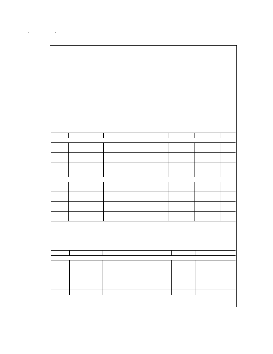
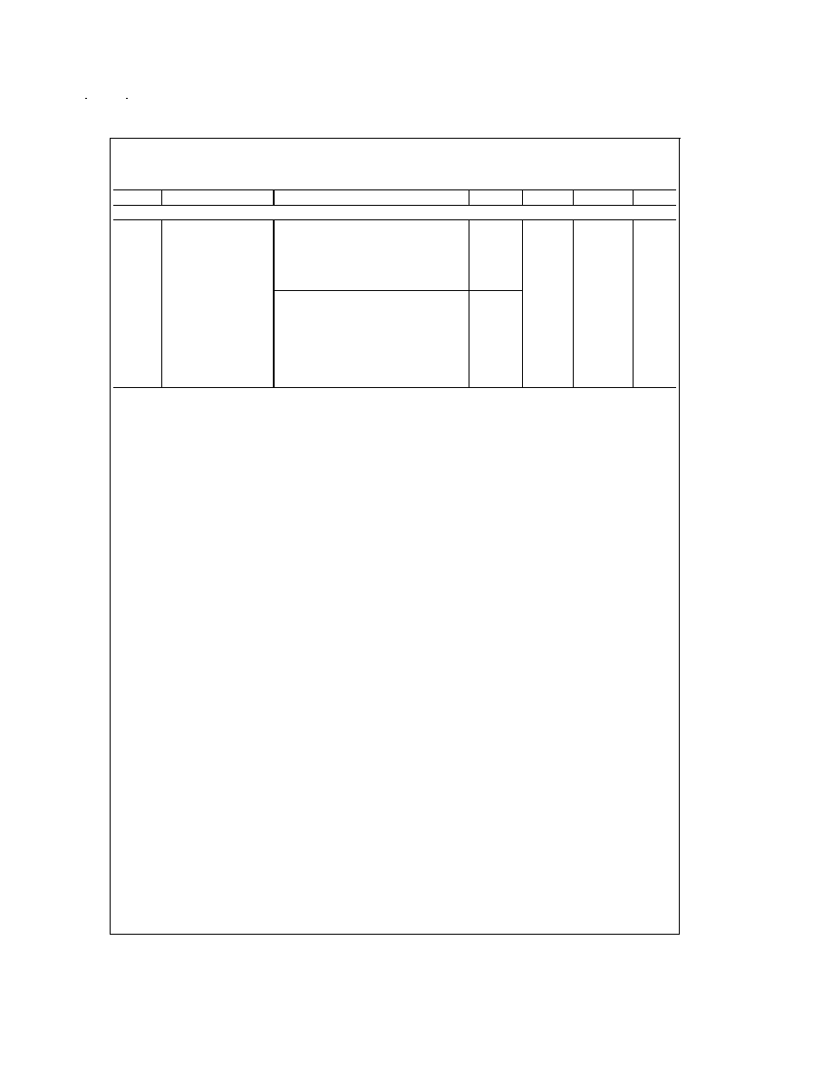
LM2587-3.3
Electrical Characteristics
Specifications with standard type face are for T
J
= 25įC, and those in bold type face apply over full Operating Temperature
Range. Unless otherwise specified, V
IN
= 5V.
Symbol
Parameters
Conditions
Typical
Min
Max
Units
SYSTEM PARAMETERS Test Circuit of
Figure 2 (Note 4)
V
OUT
Output Voltage
V
IN
= 4V to 12V
3.3
3.17/3.14
3.43/3.46
V
I
LOAD
= 400 mA to 1.75A
V
OUT
/
Line Regulation
V
IN
= 4V to 12V
20
50/100
mV
V
IN
I
LOAD
= 400 mA
V
OUT
/
Load Regulation
V
IN
= 12V
20
50/100
mV
I
LOAD
I
LOAD
= 400 mA to 1.75A
Efficiency
V
IN
= 12V, I
LOAD
= 1A
75
%
UNIQUE DEVICE PARAMETERS (Note 5)
V
REF
Output Reference
Measured at Feedback Pin
3.3
3.242/3.234
3.358/3.366
V
Voltage
V
COMP
= 1.0V
V
REF
Reference Voltage
V
IN
= 4V to 40V
2.0
mV
Line Regulation
G
M
Error Amp
I
COMP
= -30 ĶA to +30 ĶA
1.193
0.678
2.259
mmho
Transconductance
V
COMP
= 1.0V
A
VOL
Error Amp
V
COMP
= 0.5V to 1.6V
260
151/75
V/V
Voltage Gain
R
COMP
= 1.0 M
(Note 6)
LM2587-5.0
Electrical Characteristics
Specifications with standard type face are for T
J
= 25įC, and those in bold type face apply over full Operating Temperature
Range. Unless otherwise specified, V
IN
= 5V.
Symbol
Parameters
Conditions
Typical
Min
Max
Units
SYSTEM PARAMETERS Test Circuit of
Figure 2 (Note 4)
V
OUT
Output Voltage
V
IN
= 4V to 12V
5.0
4.80/4.75
5.20/5.25
V
I
LOAD
= 500 mA to 1.45A
V
OUT
/
Line Regulation
V
IN
= 4V to 12V
20
50/100
mV
V
IN
I
LOAD
= 500 mA
V
OUT
/
Load Regulation
V
IN
= 12V
20
50/100
mV
I
LOAD
I
LOAD
= 500 mA to 1.45A
Efficiency
V
IN
= 12V, I
LOAD
= 750 mA
80
%
www.national.com
2
LM2587-5.0
Electrical Characteristics
(Continued)
Symbol
Parameters
Conditions
Typical
Min
Max
Units
UNIQUE DEVICE PARAMETERS (Note 5)
V
REF
Output Reference
Measured at Feedback Pin
5.0
4.913/4.900
5.088/5.100
V
Voltage
V
COMP
= 1.0V
V
REF
Reference Voltage
V
IN
= 4V to 40V
3.3
mV
Line Regulation
G
M
Error Amp
I
COMP
= -30 ĶA to +30 ĶA
0.750
0.447
1.491
mmho
Transconductance
V
COMP
= 1.0V
A
VOL
Error Amp
V
COMP
= 0.5V to 1.6V
165
99/49
V/V
Voltage Gain
R
COMP
= 1.0 M
(Note 6)
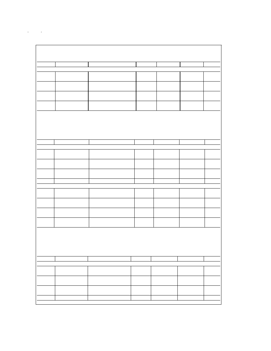
LM2587-12
Electrical Characteristics
Specifications with standard type face are for T
J
= 25įC, and those in bold type face apply over full Operating Temperature
Range. Unless otherwise specified, V
IN
= 5V.
Symbol
Parameters
Conditions
Typical
Min
Max
Units
SYSTEM PARAMETERS Test Circuit of
Figure 3 (Note 4)
V
OUT
Output Voltage
V
IN
= 4V to 10V
12.0
11.52/11.40
12.48/12.60
V
I
LOAD
= 300 mA to 1.2A
V
OUT
/
Line Regulation
V
IN
= 4V to 10V
20
100/200
mV
V
IN
I
LOAD
= 300 mA
V
OUT
/
Load Regulation
V
IN
= 10V
20
100/200
mV
I
LOAD
I
LOAD
= 300 mA to 1.2A
Efficiency
V
IN
= 10V, I
LOAD
= 1A
90
%
UNIQUE DEVICE PARAMETERS (Note 5)
V
REF
Output Reference
Measured at Feedback Pin
12.0
11.79/11.76
12.21/12.24
V
Voltage
V
COMP
= 1.0V
V
REF
Reference Voltage
V
IN
= 4V to 40V
7.8
mV
Line Regulation
G
M
Error Amp
I
COMP
= -30 ĶA to +30 ĶA
0.328
0.186
0.621
mmho
Transconductance
V
COMP
= 1.0V
A
VOL
Error Amp
V
COMP
= 0.5V to 1.6V
70
41/21
V/V
Voltage Gain
R
COMP
= 1.0 M
(Note 6)
LM2587-ADJ
Electrical Characteristics
Specifications with standard type face are for T
J
= 25įC, and those in bold type face apply over full Operating Temperature
Range. Unless otherwise specified, V
IN
= 5V.
Symbol
Parameters
Conditions
Typical
Min
Max
Units
SYSTEM PARAMETERS Test Circuit of
Figure 3 (Note 4)
V
OUT
Output Voltage
V
IN
= 4V to 10V
12.0
11.52/11.40
12.48/12.60
V
I
LOAD
= 300 mA to 1.2A
V
OUT
/
Line Regulation
V
IN
= 4V to 10V
20
100/200
mV
V
IN
I
LOAD
= 300 mA
V
OUT
/
Load Regulation
V
IN
= 10V
20
100/200
mV
I
LOAD
I
LOAD
= 300 mA to 1.2A
Efficiency
V
IN
= 10V, I
LOAD
= 1A
90
%
www.national.com
3
LM2587-ADJ
Electrical Characteristics
(Continued)
Symbol
Parameters
Conditions
Typical
Min
Max
Units
UNIQUE DEVICE PARAMETERS (Note 5)
V
REF
Output Reference
Measured at Feedback Pin
1.230
1.208/1.205
1.252/1.255
V
Voltage
V
COMP
= 1.0V
V
REF
Reference Voltage
V
IN
= 4V to 40V
1.5
mV
Line Regulation
G
M
Error Amp
I
COMP
= -30 ĶA to +30 ĶA
3.200
1.800
6.000
mmho
Transconductance
V
COMP
= 1.0V
A
VOL
Error Amp
V
COMP
= 0.5V to 1.6V
670
400/200
V/V
Voltage Gain
R
COMP
= 1.0 M
(Note 6)
I
B
Error Amp
V
COMP
= 1.0V
125
425/600
nA
Input Bias Current
All Output Voltage Versions
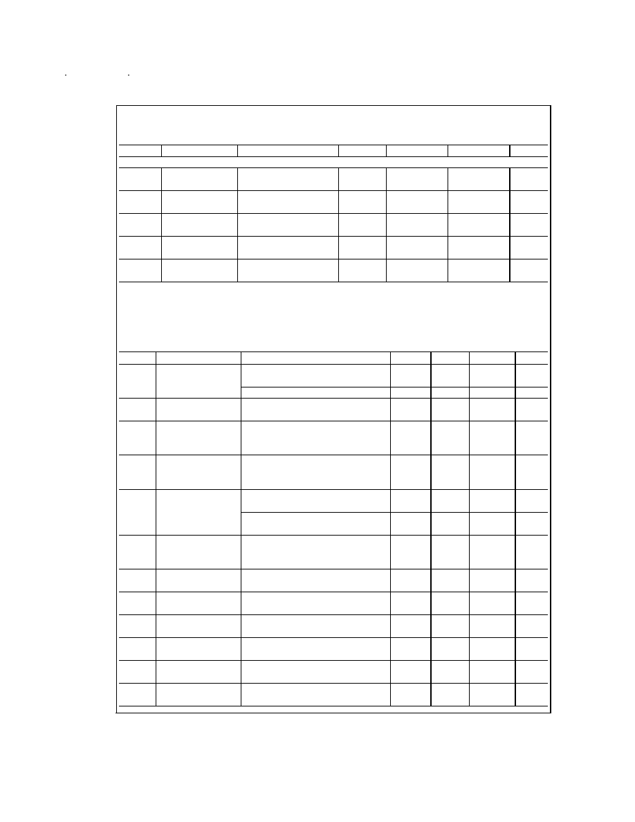
Electrical Characteristics
(Note 5)
Specifications with standard type face are for T
J
= 25įC, and those in bold type face apply over full Operating Temperature
Range. Unless otherwise specified, V
IN
= 5V.
Symbol
Parameters
Conditions
Typical
Min
Max
Units
I
S
Input Supply Current
(Switch Off)
11
15.5/16.5
mA
(Note 8)
I
SWITCH
= 3.0A
85
140
165
mA
V
UV
Input Supply
R
LOAD
= 100
3.30
3.05
3.75
V
Undervoltage Lockout
f
O
Oscillator Frequency
Measured at Switch Pin
R
LOAD
= 100
100
85/75
115/125
kHz
V
COMP
= 1.0V
f
SC
Short-Circuit
Measured at Switch Pin
Frequency
R
LOAD
= 100
25
kHz
V
FEEDBACK
= 1.15V
V
EAO
Error Amplifier
Upper Limit
2.8
2.6/2.4
V
Output Swing
(Note 7)
Lower Limit
0.25
0.40/0.55
V
(Note 8)
I
EAO
Error Amp
(Note 9)
Output Current
165
110/70
260/320
ĶA
(Source or Sink)
I
SS
Soft Start Current
V
FEEDBACK
= 0.92V
11.0
8.0/7.0
17.0/19.0
ĶA
V
COMP
= 1.0V
D
Maximum Duty Cycle
R
LOAD
= 100
98
93/90
%
(Note 7)
I
L
Switch Leakage
Switch Off
15
300/600
ĶA
Current
V
SWITCH
= 60V
V
SUS
Switch Sustaining
dV/dT = 1.5V/ns
65
V
Voltage
V
SAT
Switch Saturation
I
SWITCH
= 5.0A
0.7
1.1/1.4
V
Voltage
I
CL
NPN Switch
6.5
5.0
9.5
A
Current Limit
www.national.com
4
All Output Voltage Versions
Electrical Characteristics
(Note 5) (Continued)
Symbol
Parameters
Conditions
Typical
Min
Max
Units
COMMON DEVICE PARAMETERS (Note 4)
JA
Thermal Resistance
T Package, Junction to Ambient
(Note 10)
65
JA
T Package, Junction to Ambient
(Note 11)
45
JC
T Package, Junction to Case
2
JA
S Package, Junction to Ambient
(Note 12)
56
įC/W
JA
S Package, Junction to Ambient
(Note 13)
35
JA
S Package, Junction to Ambient
(Note 14)
26
JC
S Package, Junction to Case
2
Note 1: Absolute Maximum Ratings indicate limits beyond which damage to the device may occur. Operating ratings indicate conditions the device is intended to
be functional, but device parameter specifications may not be guaranteed under these conditions. For guaranteed specifications and test conditions, see the Electrical
Characteristics.
Note 2: Note that switch current and output current are not identical in a step-up regulator. Output current cannot be internally limited when the LM2587 is used as
a step-up regulator. To prevent damage to the switch, the output current must be externally limited to 5A. However, output current is internally limited when the
LM2587 is used as a flyback regulator (see the Application Hints section for more information).
Note 3: The junction temperature of the device (T
J
) is a function of the ambient temperature (T
A
), the junction-to-ambient thermal resistance (
JA
), and the power
dissipation of the device (P
D
). A thermal shutdown will occur if the temperature exceeds the maximum junction temperature of the device: P
D
x
JA
+ T
A(MAX)
T
J-
(MAX)
. For a safe thermal design, check that the maximum power dissipated by the device is less than: P
D
[T
J(MAX)
- T
A(MAX)
)]/
JA
. When calculating the maximum
allowable power dissipation, derate the maximum junction temperature -- this ensures a margin of safety in the thermal design.
Note 4: External components such as the diode, inductor, input and output capacitors can affect switching regulator performance. When the LM2587 is used as
shown in
Figure 2 and Figure 3, system performance will be as specified by the system parameters.
Note 5: All room temperature limits are 100% production tested, and all limits at temperature extremes are guaranteed via correlation using standard Statistical Qual-
ity Control (SQC) methods.
Note 6: A 1.0 M
resistor is connected to the compensation pin (which is the error amplifier output) to ensure accuracy in measuring A
VOL
.
Note 7: To measure this parameter, the feedback voltage is set to a low value, depending on the output version of the device, to force the error amplifier output high.
Adj: V
FB
= 1.05V; 3.3V: V
FB
= 2.81V; 5.0V: V
FB
= 4.25V; 12V: V
FB
= 10.20V.
Note 8: To measure this parameter, the feedback voltage is set to a high value, depending on the output version of the device, to force the error amplifier output low.
Adj: V
FB
= 1.41V; 3.3V: V
FB
= 3.80V; 5.0V: V
FB
= 5.75V; 12V: V
FB
= 13.80V.
Note 9: To measure the worst-case error amplifier output current, the LM2587 is tested with the feedback voltage set to its low value (specified in Note 7) and at its
high value (specified in Note 8).
Note 10: Junction to ambient thermal resistance (no external heat sink) for the 5 lead TO-220 package mounted vertically, with
1
/
2
inch leads in a socket, or on a PC
board with minimum copper area.
Note 11: Junction to ambient thermal resistance (no external heat sink) for the 5 lead TO-220 package mounted vertically, with
1
/
2
inch leads soldered to a PC board
containing approximately 4 square inches of (1oz.) copper area surrounding the leads.
Note 12: Junction to ambient thermal resistance for the 5 lead TO-263 mounted horizontally against a PC board area of 0.136 square inches (the same size as the
TO-263 package) of 1 oz. (0.0014 in. thick) copper.
Note 13: Junction to ambient thermal resistance for the 5 lead TO-263 mounted horizontally against a PC board area of 0.4896 square inches (3.6 times the area
of the TO-263 package) of 1 oz. (0.0014 in. thick) copper.
Note 14: Junction to ambient thermal resistance for the 5 lead TO-263 mounted horizontally against a PC board copper area of 1.0064 square inches (7.4 times the
area of the TO-263 package) of 1 oz. (0.0014 in. thick) copper. Additional copper area will reduce thermal resistance further. See the thermal model in Switchers Made
Simple
ģ
software.
www.national.com
5
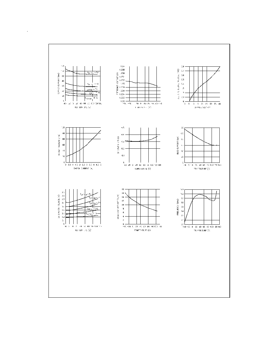
Typical Performance Characteristics
Supply Current
vs Temperature
DS012316-48
Reference Voltage
vs Temperature
DS012316-49
Reference Voltage
vs Supply Voltage
DS012316-50
Supply Current
vs Switch Current
DS012316-51
Current Limit
vs Temperature
DS012316-52
Feedback Pin Bias
Current vs Temperature
DS012316-53
Switch Saturation
Voltage vs Temperature
DS012316-54
Switch Transconductance
vs Temperature
DS012316-55
Oscillator Frequency
vs Temperature
DS012316-56
www.national.com
6
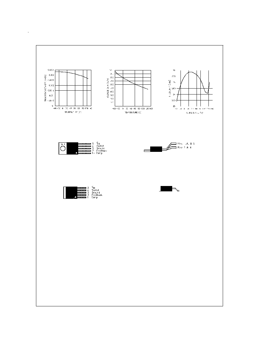
Typical Performance Characteristics
(Continued)
Connection Diagrams
Error Amp Transconductance
vs Temperature
DS012316-57
Error Amp Voltage
Gain vs Temperature
DS012316-58
Short Circuit Frequency
vs Temperature
DS012316-59
Bent, Staggered Leads
5-Lead TO-220 (T)
Top View
DS012316-3
Bent, Staggered Leads
5-Lead TO-220 (T)
Side View
DS012316-4
Order Number LM2587T-3.3, LM2587T-5.0,
LM2587T-12 or LM2587T-ADJ
See NS Package Number T05D
5-Lead TO-263 (S)
Top View
DS012316-5
5-Lead TO-263 (S)
Side View
DS012316-6
Order Number LM2587S-3.3, LM2587S-5.0,
LM2587S-12 or LM2587S-ADJ
See NS Package Number TS5B
www.national.com
7

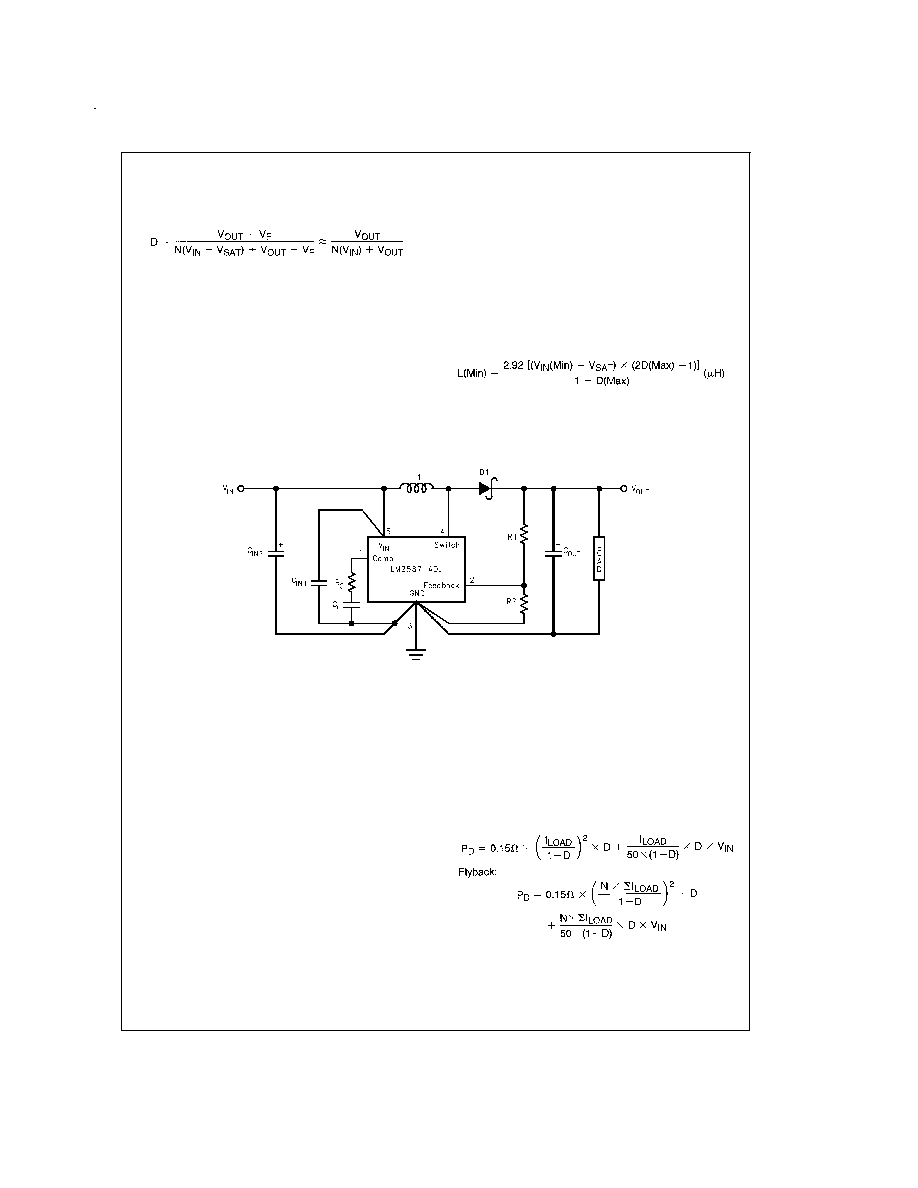
Block Diagram
DS012316-7
For Fixed Versions
3.3V, R1 = 3.4k, R2 = 2k
5V, R1 = 6.15k, R2 = 2k
12V, R1 = 8.73k, R2 = 1k
For Adj. Version
R1 = Short (0
), R2 = Open
FIGURE 1.
www.national.com
8

Test Circuits
DS012316-8
C
IN1
-- 100 ĶF, 25V Aluminum Electrolytic
C
IN2
-- 0.1 ĶF Ceramic
T -- 22 ĶH, 1:1 Schott #67141450
D -- 1N5820
C
OUT
-- 680 ĶF, 16V Aluminum Electrolytic
C
C
-- 0.47 ĶF Ceramic
R
C
-- 2k
FIGURE 2. LM2587-3.3 and LM2587-5.0
DS012316-9
C
IN1
-- 100 ĶF, 25V Aluminum Electrolytic
C
IN2
-- 0.1 ĶF Ceramic
L -- 15 ĶH, Renco #RL-5472-5
D -- 1N5820
C
OUT
-- 680 ĶF, 16V Aluminum Electrolytic
C
C
-- 0.47 ĶF Ceramic
R
C
-- 2k
For 12V Devices: R
1
= Short (0
) and R
2
= Open
For ADJ Devices: R
1
= 48.75k,
Ī
0.1% and R2 = 5.62k,
Ī
1%
FIGURE 3. LM2587-12 and LM2587-ADJ
www.national.com
9
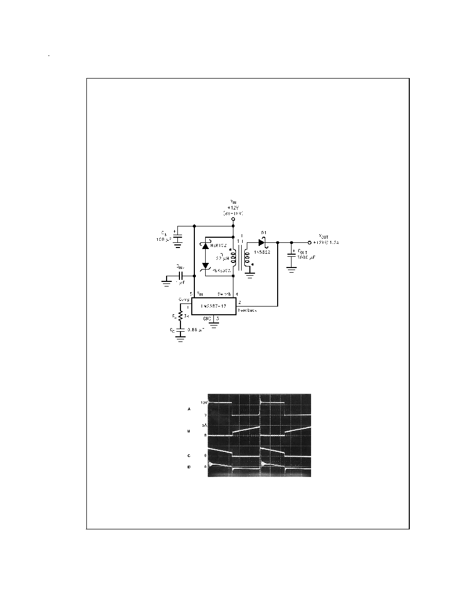
Flyback Regulator Operation
The LM2587 is ideally suited for use in the flyback regulator
topology. The flyback regulator can produce a single output
voltage, such as the one shown in
Figure 4, or multiple out-
put voltages. In
Figure 4, the flyback regulator generates an
output voltage that is inside the range of the input voltage.
This feature is unique to flyback regulators and cannot be
duplicated with buck or boost regulators.
The operation of a flyback regulator is as follows (refer to
Figure 4): when the switch is on, current flows through the
primary winding of the transformer, T1, storing energy in the
magnetic field of the transformer. Note that the primary and
secondary windings are out of phase, so no current flows
through the secondary when current flows through the pri-
mary. When the switch turns off, the magnetic field col-
lapses, reversing the voltage polarity of the primary and sec-
ondary windings. Now rectifier D1 is forward biased and
current flows through it, releasing the energy stored in the
transformer. This produces voltage at the output.
The output voltage is controlled by modulating the peak
switch current. This is done by feeding back a portion of the
output voltage to the error amp, which amplifies the differ-
ence between the feedback voltage and a 1.230V reference.
The error amp output voltage is compared to a ramp voltage
proportional to the switch current (i.e., inductor current dur-
ing the switch on time). The comparator terminates the
switch on time when the two voltages are equal, thereby
controlling the peak switch current to maintain a constant
output voltage.
Typical Performance Characteristics
DS012316-10
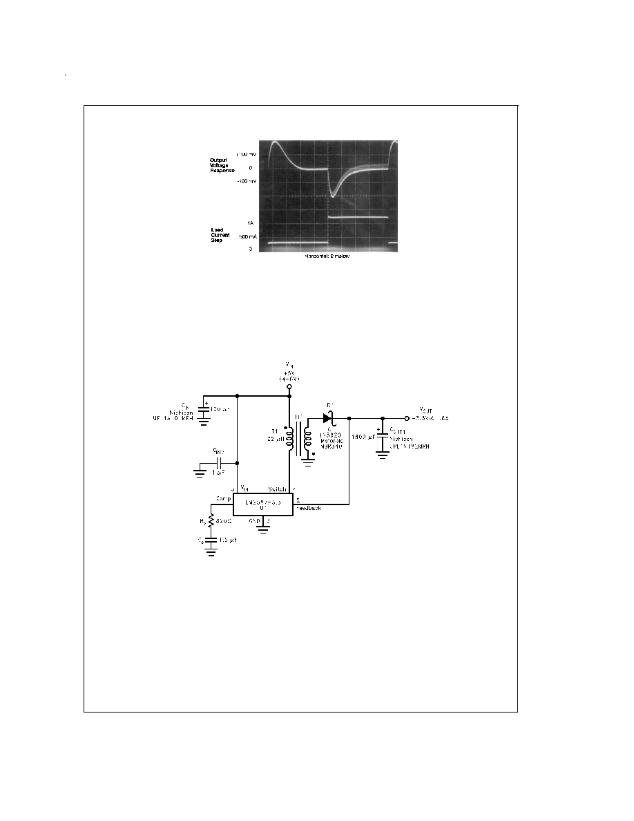
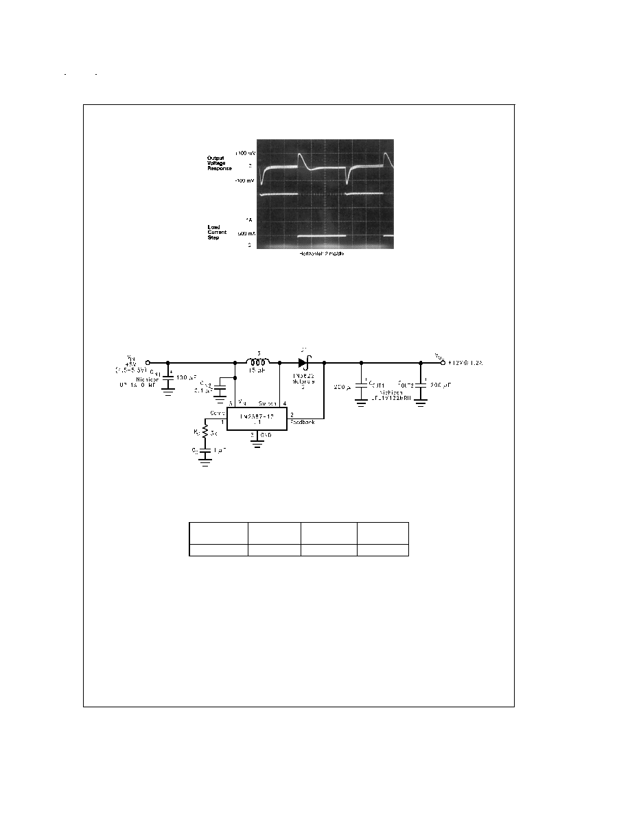
As shown in
Figure 4, the LM2587 can be used as a flyback regulator by using a minimum number of external components. The switching waveforms of this
regulator are shown in
Figure 5. Typical Performance Characteristics observed during the operation of this circuit are shown in Figure 6.
FIGURE 4. 12V Flyback Regulator Design Example
DS012316-11
A: Switch Voltage, 10 V/div
B: Switch Current, 5 A/div
C: Output Rectifier Current, 5 A/div
D: Output Ripple Voltage, 100 mV/div
AC-Coupled
Horizontal: 2 Ķs/div
FIGURE 5. Switching Waveforms
www.national.com
10
Typical Performance Characteristics
(Continued)
Typical Flyback Regulator Applications
Figures 7, 8, 9, 11, 12 show six typical flyback applications,
varying from single output to triple output. Each drawing con-
tains the part number(s) and manufacturer(s) for every com-
ponent except the transformer. For the transformer part
numbers and manufacturers names, see the table in
Figure
13.
For
applications
with
different
output
voltages -- requiring the LM2587-ADJ -- or different output
configurations that do not match the standard configurations,
refer to the
Switchers Made Simple software.
DS012316-12
FIGURE 6. V
OUT
Load Current Step Response
DS012316-13
FIGURE 7. Single-Output Flyback Regulator
www.national.com
11
Typical Flyback Regulator Applications
(Continued)
DS012316-14
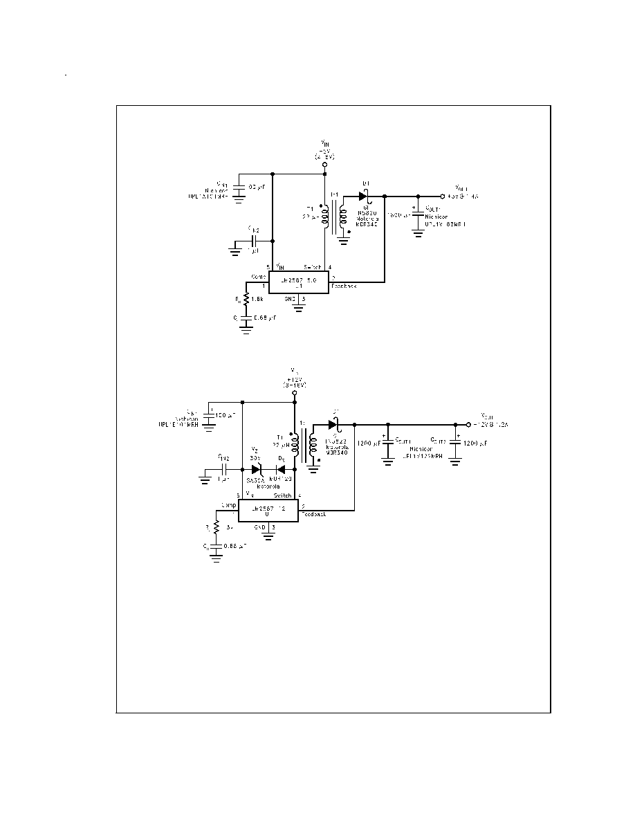
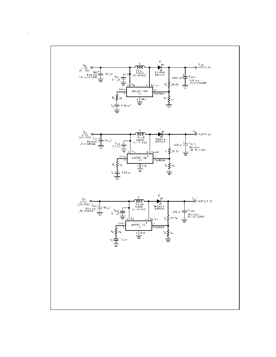
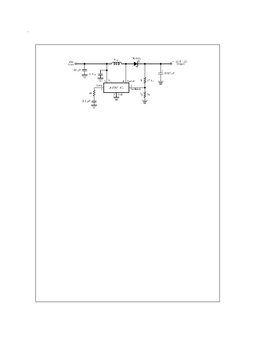
FIGURE 8. Single-Output Flyback Regulator
DS012316-15
FIGURE 9. Single-Output Flyback Regulator
www.national.com
12
Typical Flyback Regulator Applications
(Continued)
DS012316-16
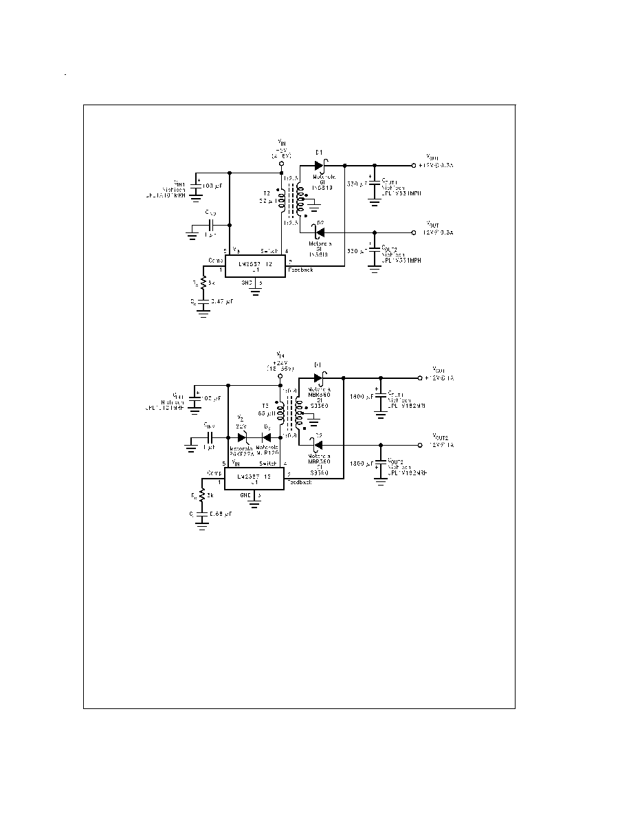
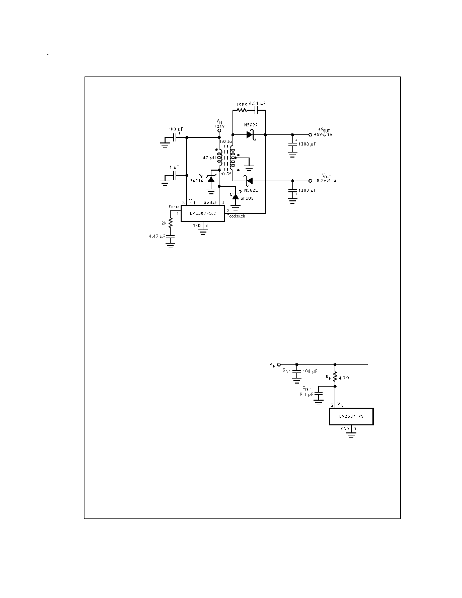
FIGURE 10. Dual-Output Flyback Regulator
DS012316-17
FIGURE 11. Dual-Output Flyback Regulator
www.national.com
13
Typical Flyback Regulator Applications
(Continued)
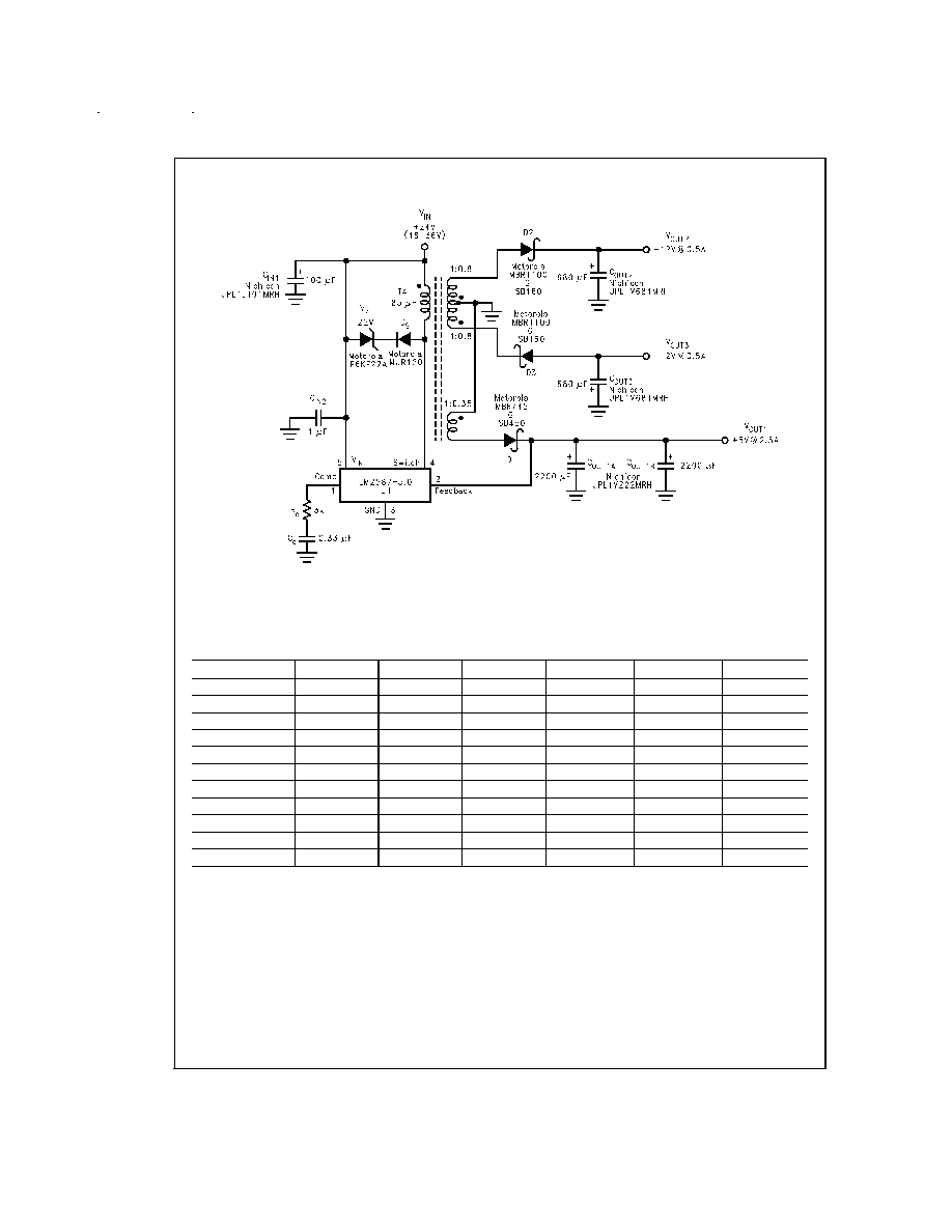
Transformer Selection (T)
Figure 13 lists the standard transformers available for flyback regulator applications. Included in the table are the turns ratio(s) for
each transformer, as well as the output voltages, input voltage ranges, and the maximum load currents for each circuit.
DS012316-18
FIGURE 12. Triple-Output Flyback Regulator
Applications
Figure 7
Figure 8
Figure 9
Figure 10
Figure 11
Figure 12
Transformers
T1
T1
T1
T2
T3
T4
V
IN
4V≠6V
4V≠6V
8V≠16V
4V≠6V
18V≠36V
18V≠36V
V
OUT1
3.3V
5V
12V
12V
12V
5V
I
OUT1
(Max)
1.8A
1.4A
1.2A
0.3A
1A
2.5A
N
1
1
1
1
2.5
0.8
0.35
V
OUT2
-12V
-12V
12V
I
OUT2
(Max)
0.3A
1A
0.5A
N
2
2.5
0.8
0.8
V
OUT3
-12V
I
OUT3
(Max)
0.5A
N
3
0.8
FIGURE 13. Transformer Selection Table
www.national.com
14
Typical Flyback Regulator Applications
(Continued)
Transformer Footprints
Figures 15, 16, 17, 18, 19, 20, 21, 22, 23, 24, 25, 26, 27, 28, 29, 30, 31 and Figure 32 show the footprints of each transformer,
listed in
Figure 14.
Transformer
Type
Manufacturers' Part Numbers
Coilcraft
Coilcraft (Note 15)
Pulse (Note 16)
Renco
Schott
(Note 15)
Surface Mount
Surface Mount
(Note 17)
(Note 18)
T1
Q4434-B
Q4435-B
PE-68411
RL-5530
67141450
T2
Q4337-B
Q4436-B
PE-68412
RL-5531
67140860
T3
Q4343-B
--
PE-68421
RL-5534
67140920
T4
Q4344-B
--
PE-68422
RL-5535
67140930
Note 15: Coilcraft Inc.,:
Phone: (800) 322-2645
1102 Silver Lake Road, Cary, IL 60013:
Fax: (708) 639-1469
Note 16: Pulse Engineering Inc.,:
Phone: (619) 674-8100
12220 World Trade Drive, San Diego, CA 92128:
Fax: (619) 674-8262
Note 17: Renco Electronics Inc.,:
Phone: (800) 645-5828
60 Jeffryn Blvd. East, Deer Park, NY 11729:
Fax: (516) 586-5562
Note 18: Schott Corp.,:
Phone: (612) 475-1173
1000 Parkers Lane Road, Wayzata, MN 55391:
Fax: (612) 475-1786
FIGURE 14. Transformer Manufacturer Guide
T1
DS012316-30
Top View
FIGURE 15. Coilcraft Q4434-B
T2
DS012316-31
Top View
FIGURE 16. Coilcraft Q4337-B
T3
DS012316-32
Top View
FIGURE 17. Coilcraft Q4343-B
T4
DS012316-33
Top View
FIGURE 18. Coilcraft Q4344-B
T1
DS012316-34
Top View
FIGURE 19. Coilcraft Q4435-B
(Surface Mount)
www.national.com
15
Typical Flyback Regulator
Applications
(Continued)
T2
DS012316-35
Top View
FIGURE 20. Coilcraft Q4436-B
(Surface Mount)
T1
DS012316-36
Top View
FIGURE 21. Pulse PE-68411
(Surface Mount)
T2
DS012316-37
Top View
FIGURE 22. Pulse PE-68412
(Surface Mount)
T3
DS012316-38
Top View
FIGURE 23. Pulse PE-68421
(Surface Mount)
T4
DS012316-39
Top View
FIGURE 24. Pulse PE-68422
(Surface Mount)
T1
DS012316-40
Top View
FIGURE 25. Renco RL-5530
T2
DS012316-41
Top View
FIGURE 26. Renco RL-5531
T3
DS012316-46
Top View
FIGURE 27. Renco RL-5534
www.national.com
16
Typical Flyback Regulator
Applications
(Continued)
T4
DS012316-42
Top View
FIGURE 28. Renco RL-5535
T1
DS012316-43
Top View
FIGURE 29. Schott 67141450
T2
DS012316-44
Top View
FIGURE 30. Schott 67140860
T3
DS012316-45
Top View
FIGURE 31. Schott 67140920
T4
DS012316-47
Top View
FIGURE 32. Schott 67140930
www.national.com
17
Step-Up (Boost) Regulator Operation
Figure 33 shows the LM2587 used as a step-up (boost)
regulator. This is a switching regulator that produces an out-
put voltage greater than the input supply voltage.
A brief explanation of how the LM2587 Boost Regulator
works is as follows (refer to
Figure 33). When the NPN
switch turns on, the inductor current ramps up at the rate of
V
IN
/L, storing energy in the inductor. When the switch turns
off, the lower end of the inductor flies above V
IN
, discharging
its current through diode (D) into the output capacitor (C
OUT
)
at a rate of (V
OUT
- V
IN
)/L. Thus, energy stored in the induc-
tor during the switch on time is transferred to the output dur-
ing the switch off time. The output voltage is controlled by
adjusting the peak switch current, as described in the flyback
regulator section.
Typical Performance Characteristics
DS012316-19
By adding a small number of external components (as shown in
Figure 33), the LM2587 can be used to produce a regulated output voltage that is greater than
the applied input voltage. The switching waveforms observed during the operation of this circuit are shown in
Figure 34. Typical performance of this regulator is
shown in
Figure 35.
FIGURE 33. 12V Boost Regulator
DS012316-20
A: Switch Voltage, 10 V/div
B: Switch Current, 5 A/div
C: Inductor Current, 5 A/div
D: Output Ripple Voltage,
100 mV/div, AC-Coupled
Horizontal: 2 Ķs/div
FIGURE 34. Switching Waveforms
www.national.com
18
Typical Performance Characteristics
(Continued)
Typical Boost Regulator Applications
Figure 36 and Figures 38, 39 and Figure 40 show four typical
boost applications) -- one fixed and three using the adjust-
able version of the LM2587. Each drawing contains the part
number(s) and manufacturer(s) for every component. For
the fixed 12V output application, the part numbers and
manufacturers' names for the inductor are listed in a table in
Figure 40. For applications with different output voltages, re-
fer to the
Switchers Made Simple software.
Figure 37 contains a table of standard inductors, by part number and corresponding manufacturer, for the fixed output regulator
of
Figure 36.
DS012316-21
FIGURE 35. V
OUT
Response to Load Current Step
DS012316-22
FIGURE 36. +5V to +12V Boost Regulator
Coilcraft
(Note 19)
Pulse
(Note 20)
Renco
(Note 21)
Schott
(Note 22)
R4793-A
PE-53900
RL-5472-5
67146520
Note 19: Coilcraft Inc.,:
Phone: (800) 322-2645
1102 Silver Lake Road, Cary, IL 60013:
Fax: (708) 639-1469
Note 20: Pulse Engineering Inc.,:
Phone: (619) 674-8100
12220 World Trade Drive, San Diego, CA 92128:
Fax: (619) 674-8262
Note 21: Renco Electronics Inc.,:
Phone: (800) 645-5828
60 Jeffryn Blvd. East, Deer Park, NY 11729:
Fax: (516) 586-5562
Note 22: Schott Corp.,:
Phone: (612) 475-1173
1000 Parkers Lane Road, Wayzata, MN 55391:
Fax: (612) 475-1786
FIGURE 37. Inductor Selection Table
www.national.com
19
Typical Boost Regulator Applications
(Continued)
DS012316-23
FIGURE 38. +12V to +24V Boost Regulator
DS012316-24
FIGURE 39. +24V to +36V Boost Regulator
DS012316-25
*
The LM2587 will require a heat sink in these applications. The size of the heat sink will depend on the maximum ambient temperature. To calculate the thermal
resistance of the IC and the size of the heat sink needed, see the "Heat Sink/Thermal Considerations" section in the Application Hints.
FIGURE 40. +24V to +48V Boost Regulator
www.national.com
20
Application Hints
PROGRAMMING OUTPUT VOLTAGE
(SELECTING R
1
AND R
2
)
Referring to the adjustable regulator in
Figure 41, the output
voltage is programmed by the resistors R
1
and R
2
by the fol-
lowing formula:
V
OUT
= V
REF
(1 + R
1
/R
2
)
where V
REF
= 1.23V
Resistors R
1
and R
2
divide the output voltage down so that
it can be compared with the 1.23V internal reference. With
R
2
between 1k and 5k, R
1
is:
R
1
= R
2
(V
OUT
/V
REF
- 1)
where V
REF
= 1.23V
For best temperature coefficient and stability with time, use
1% metal film resistors.
SHORT CIRCUIT CONDITION
Due to the inherent nature of boost regulators, when the out-
put is shorted (see
Figure 41), current flows directly from the
input, through the inductor and the diode, to the output, by-
passing the switch. The current limit of the switch
does not
limit the output current for the entire circuit. To protect the
load and prevent damage to the switch, the current must be
externally limited, either by the input supply or at the output
with an external current limit circuit. The external limit should
be set to the maximum switch current of the device, which is
5A.
In a flyback regulator application (
Figure 42), using the stan-
dard transformers, the LM2587 will survive a short circuit to
the main output. When the output voltage drops to 80% of its
nominal value, the frequency will drop to 25 kHz. With a
lower frequency, off times are larger. With the longer off
times, the transformer can release all of its stored energy be-
fore the switch turns back on. Hence, the switch turns on ini-
tially with zero current at its collector. In this condition, the
switch current limit will limit the peak current, saving the de-
vice.
FLYBACK REGULATOR INPUT CAPACITORS
A flyback regulator draws discontinuous pulses of current
from the input supply. Therefore, there are two input capaci-
tors needed in a flyback regulator; one for energy storage
and one for filtering (see
Figure 42). Both are required due to
the inherent operation of a flyback regulator. To keep a
stable or constant voltage supply to the LM2587, a storage
capacitor (
100 ĶF) is required. If the input source is a reciti-
fied DC supply and/or the application has a wide tempera-
ture range, the required rms current rating of the capacitor
might be very large. This means a larger value of capaci-
tance or a higher voltage rating will be needed of the input
capacitor. The storage capacitor will also attenuate noise
which may interfere with other circuits connected to the
same input supply voltage.
DS012316-26
FIGURE 41. Boost Regulator
www.national.com
21
Application Hints
(Continued)
In addition, a small bypass capacitor is required due to the
noise generated by the input current pulses. To eliminate the
noise, insert a 1.0 ĶF ceramic capacitor between V
IN
and
ground as close as possible to the device.
SWITCH VOLTAGE LIMITS
In a flyback regulator, the maximum steady-state voltage ap-
pearing at the switch, when it is off, is set by the transformer
turns ratio, N, the output voltage, V
OUT
, and the maximum in-
put voltage, V
IN
(Max):
V
SW(OFF)
= V
IN
(Max) + (V
OUT
+V
F
)/N
where V
F
is the forward biased voltage of the output diode,
and is 0.5V for Schottky diodes and 0.8V for ultra-fast recov-
ery diodes (typically). In certain circuits, there exists a volt-
age spike, V
LL
, superimposed on top of the steady-state volt-
age (see
Figure 5, waveform A). Usually, this voltage spike is
caused by the transformer leakage inductance and/or the
output rectifier recovery time. To "clamp" the voltage at the
switch from exceeding its maximum value, a transient sup-
pressor in series with a diode is inserted across the trans-
former primary (as shown in the circuit on the front page and
other flyback regulator circuits throughout the datasheet).
The schematic in
Figure 42 shows another method of clamp-
ing the switch voltage. A single voltage transient suppressor
(the SA51A) is inserted at the switch pin. This method
clamps the total voltage across the switch, not just the volt-
age across the primary.
If poor circuit layout techniques are used (see the "Circuit
Layout Guideline" section), negative voltage transients may
appear on the Switch pin (pin 4). Applying a negative voltage
(with respect to the IC's ground) to any monolithic IC pin
causes erratic and unpredictable operation of that IC. This
holds true for the LM2587 IC as well. When used in a flyback
regulator, the voltage at the Switch pin (pin 4) can go nega-
tive when the switch turns on. The "ringing" voltage at the
switch pin is caused by the output diode capacitance and the
transformer leakage inductance forming a resonant circuit at
the secondary(ies). The resonant circuit generates the "ring-
ing" voltage, which gets reflected back through the trans-
former to the switch pin. There are two common methods to
avoid this problem. One is to add an RC snubber around the
output rectifier(s), as in
Figure 42. The values of the resistor
and the capacitor must be chosen so that the voltage at the
Switch pin does not drop below -0.4V. The resistor may
range in value between 10
and 1 k
, and the capacitor will
vary from 0.001 ĶF to 0.1 ĶF. Adding a snubber will (slightly)
reduce the efficiency of the overall circuit.
The other method to reduce or eliminate the "ringing" is to in-
sert a Schottky diode clamp between pins 4 and 3 (ground),
also shown in
Figure 42. This prevents the voltage at pin 4
from dropping below -0.4V. The reverse voltage rating of the
diode must be greater than the switch off voltage.
OUTPUT VOLTAGE LIMITATIONS
The maximum output voltage of a boost regulator is the
maximum switch voltage minus a diode drop. In a flyback
regulator, the maximum output voltage is determined by the
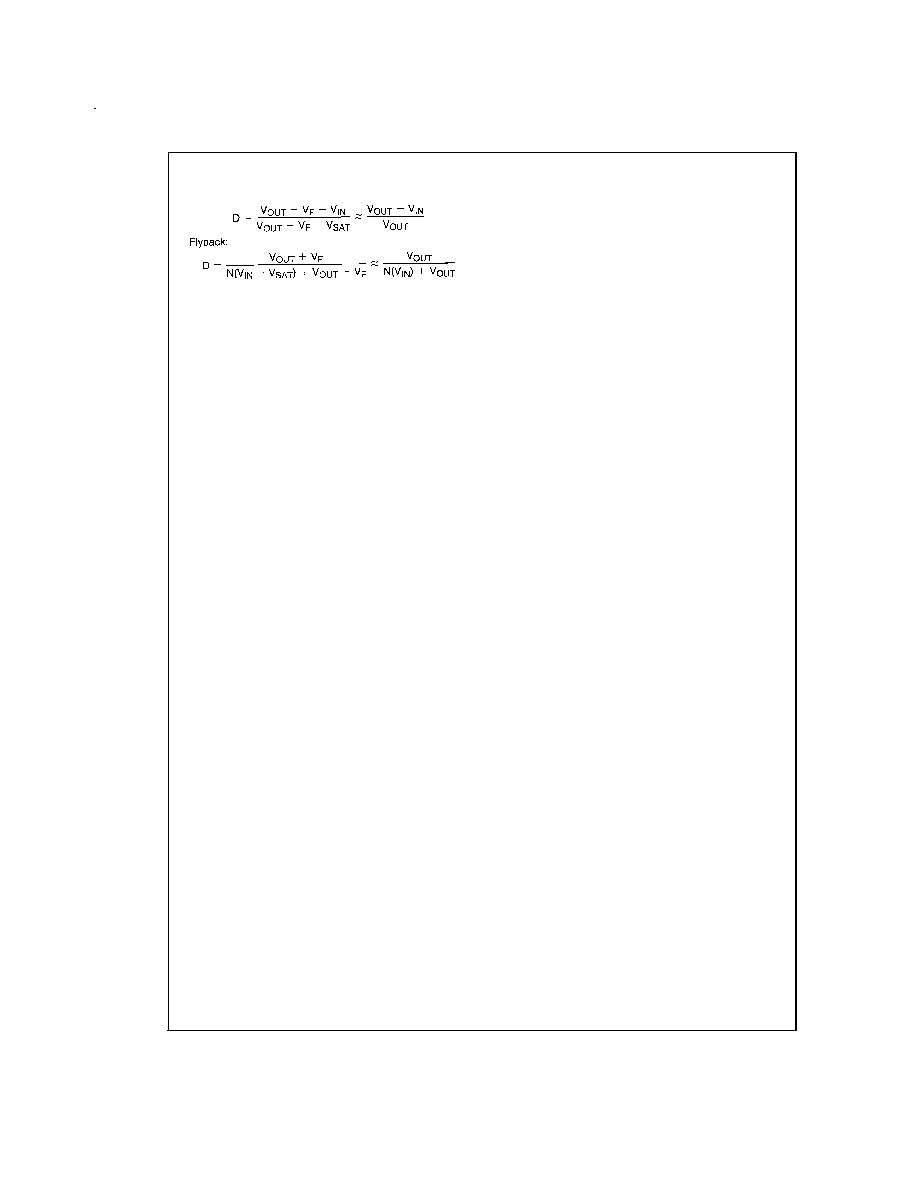
turns ratio, N, and the duty cycle, D, by the equation:
V
OUT
N x V
IN
x D/(1 - D)
DS012316-27
FIGURE 42. Flyback Regulator
DS012316-28
FIGURE 43. Input Line Filter
www.national.com
22
Application Hints
(Continued)
The duty cycle of a flyback regulator is determined by the fol-
lowing equation:
Theoretically, the maximum output voltage can be as large
as desired -- just keep increasing the turns ratio of the trans-
former. However, there exists some physical limitations that
prevent the turns ratio, and thus the output voltage, from in-
creasing to infinity. The physical limitations are capacitances
and inductances in the LM2587 switch, the output diode(s),
and the transformer -- such as reverse recovery time of the
output diode (mentioned above).
NOISY INPUT LINE CONDITION)
A small, low-pass RC filter should be used at the input pin of
the LM2587 if the input voltage has an unusual large amount
of transient noise, such as with an input switch that bounces.
The circuit in
Figure 43 demonstrates the layout of the filter,
with the capacitor placed from the input pin to ground and
the resistor placed between the input supply and the input
pin. Note that the values of R
IN
and C
IN
shown in the sche-
matic are good enough for most applications, but some read-
justing might be required for a particular application. If effi-
ciency is a major concern, replace the resistor with a small
inductor (say 10 ĶH and rated at 100 mA).
STABILITY
All current-mode controlled regulators can suffer from an in-
stability, known as subharmonic oscillation, if they operate
with a duty cycle above 50%. To eliminate subharmonic os-
cillations, a minimum value of inductance is required to en-
sure stability for all boost and flyback regulators. The mini-
mum inductance is given by:
where V
SAT
is the switch saturation voltage and can be
found in the Characteristic Curves.
CIRCUIT LAYOUT GUIDELINES
As in any switching regulator, layout is very important. Rap-
idly switching currents associated with wiring inductance
generate voltage transients which can cause problems. For
minimal inductance and ground loops, keep the length of the
leads and traces as short as possible. Use single point
grounding or ground plane construction for best results.
Separate the signal grounds from the power grounds (as in-
dicated in
Figure 44). When using the Adjustable version,
physically locate the programming resistors as near the
regulator IC as possible, to keep the sensitive feedback wir-
ing short.
HEAT SINK/THERMAL CONSIDERATIONS
In many cases, no heat sink is required to keep the LM2587
junction temperature within the allowed operating range. For
each application, to determine whether or not a heat sink will
be required, the following must be identified:
1) Maximum ambient temperature (in the application).
2) Maximum regulator power dissipation (in the application).
3) Maximum allowed junction temperature (125įC for the
LM2587). For a safe, conservative design, a temperature ap-
proximately 15įC cooler than the maximum junction tem-
perature should be selected (110įC).
4) LM2587 package thermal resistances
JA
and
JC
(given
in the Electrical Characteristics).
Total power dissipated (P
D
) by the LM2587 can be estimated
as follows:
Boost:
V
IN
is the minimum input voltage, V
OUT
is the output voltage,
N is the transformer turns ratio, D is the duty cycle, and I
LOAD
is the maximum load current (and
I
LOAD
is the sum of the
maximum load currents for multiple-output flyback regula-
tors). The duty cycle is given by:
DS012316-29
FIGURE 44. Circuit Board Layout
www.national.com
23
Application Hints
(Continued)
Boost:
where V
F
is the forward biased voltage of the diode and is
typically 0.5V for Schottky diodes and 0.8V for fast recovery
diodes. V
SAT
is the switch saturation voltage and can be
found in the Characteristic Curves.
When no heat sink is used, the junction temperature rise is:
T
J
= P
D
x
JA
.
Adding the junction temperature rise to the maximum ambi-
ent temperature gives the actual operating junction tempera-
ture:
T
J
=
T
J
+ T
A
.
If the operating junction temperature exceeds the maximum
junction temperatue in item 3 above, then a heat sink is re-
quired. When using a heat sink, the junction temperature rise
can be determined by the following:
T
J
= P
D
x (
JC
+
Interface
+
Heat Sink
)
Again, the operating junction temperature will be:
T
J
=
T
J
+ T
A
As before, if the maximum junction temperature is exceeded,
a larger heat sink is required (one that has a lower thermal
resistance).
Included in the
Switchers Made Simple design software is
a more precise (non-linear) thermal model that can be used
to determine junction temperature with different input-output
parameters or different component values. It can also calcu-
late the heat sink thermal resistance required to maintain the
regulator junction temperature below the maximum operat-
ing temperature.
To further simplify the flyback regulator design procedure,
National Semiconductor is making available computer de-
sign software. Switchers Made Simple software is available
on a (3
1
/
2
") diskette for IBM compatable computers from a
National Semiconductor sales office in your area or the Na-
tional
Semiconductor
Customer
Response
Center
(1-800-272-9959).
European Magnetic Vendor
Contacts
Please contact the following addresses for details of local
distributors or representatives:
Coilcraft
21 Napier Place
Wardpark North
Cumbernauld, Scotland G68 0LL
Phone: +44 1236 730 595
Fax: +44 1236 730 627
Pulse Engineering
Dunmore Road
Tuam
Co. Galway, Ireland
Phone: +353 93 24 107
Fax: +353 93 24 459
www.national.com
24
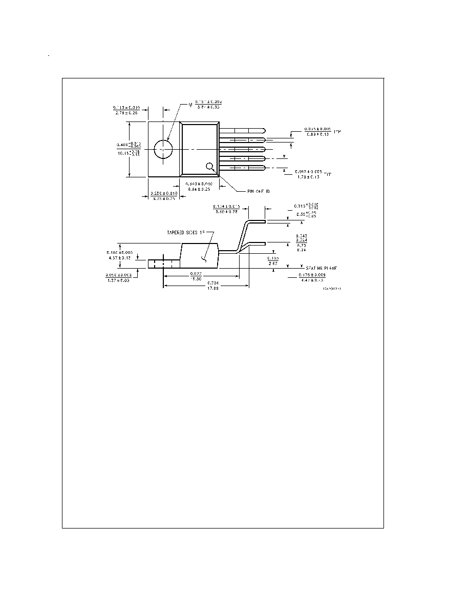
Physical Dimensions
inches (millimeters) unless otherwise noted
Order Number LM2587T-3.3, LM2587T-5.0,
LM2587T-12 or LM2587T-ADJ
NS Package Number T05D
www.national.com
25
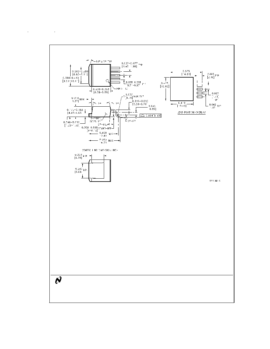
Physical Dimensions
inches (millimeters) unless otherwise noted (Continued)
LIFE SUPPORT POLICY
NATIONAL'S PRODUCTS ARE NOT AUTHORIZED FOR USE AS CRITICAL COMPONENTS IN LIFE SUPPORT DE-
VICES OR SYSTEMS WITHOUT THE EXPRESS WRITTEN APPROVAL OF THE PRESIDENT OF NATIONAL SEMI-
CONDUCTOR CORPORATION. As used herein:
1. Life support devices or systems are devices or sys-
tems which, (a) are intended for surgical implant into
the body, or (b) support or sustain life, and whose fail-
ure to perform when properly used in accordance
with instructions for use provided in the labeling, can
be reasonably expected to result in a significant injury
to the user.
2. A critical component is any component of a life support
device or system whose failure to perform can be rea-
sonably expected to cause the failure of the life support
device or system, or to affect its safety or effectiveness.
National Semiconductor
Corporation
Americas
Tel: 1-800-272-9959
Fax: 1-800-737-7018
Email: support@nsc.com
www.national.com
National Semiconductor
Europe
Fax: +49 (0) 1 80-530 85 86
Email: europe.support@nsc.com
Deutsch Tel: +49 (0) 1 80-530 85 85
English
Tel: +49 (0) 1 80-532 78 32
FranÁais Tel: +49 (0) 1 80-532 93 58
Italiano
Tel: +49 (0) 1 80-534 16 80
National Semiconductor
Asia Pacific Customer
Response Group
Tel: 65-2544466
Fax: 65-2504466
Email: sea.support@nsc.com
National Semiconductor
Japan Ltd.
Tel: 81-3-5639-7560
Fax: 81-3-5639-7507
Order Number LM2587S-3.3, LM2587S-5.0,
LM2587S-12 or LM2587S-ADJ
NS Package Number TS5B
LM2587
SIMPLE
SWITCHER
5A
Flyback
Regulator
National does not assume any responsibility for use of any circuitry described, no circuit patent licenses are implied and National reserves the right at any time without notice to change said circuitry and specifications.