LM2601
Adapter Interface Circuit
General Description
The Adapter Interface Circuit (AIC) is used to sense the
presence of an external power source for a portable com-
puter. It notifies the computer if a source is present and
indicates if the source is appropriate for charging battery
packs inside the computer. The AIC also senses an adapter
current and its direction. AIC isolates the adapter and signals
the computer when peak current threshold is exceeded.
LM2601 drives P-channel FETs. No high current rated
Schottky diode is required to implement an adapter switcho-
ver circuit. This significantly decreases additional heat dissi-
pation during simultaneous fast battery charging while run-
ning a computer, particularly in Maximum Performance
mode of operation
Features
n
Detects an AC-DC adapter suitable for battery charging
or an airplane or car power line adapter that should not
be used for battery charging
n
Allows the implementation of intelligent switchover
circuits for portable systems
n
LM2601 shuts down automatically when adapter is
removed
n
Low leakage current from battery when not powered
n
Drives P-channel FETs, no Schottky diodes are required
n
No reverse inrush current from battery into the adapter
output capacitance
n
Allows for battery capacity gas-gauge calibration under
system software/firmware control
n
Adapter over current threshold programmable with
external resistors
n
Wide input range: 5V - 24V
n
Available in TSSOP-14 package
Applications
n
Portable Computers
n
Portable IAs (Internet Appliances, Information
Appliances)
n
Other Battery Powered Devices
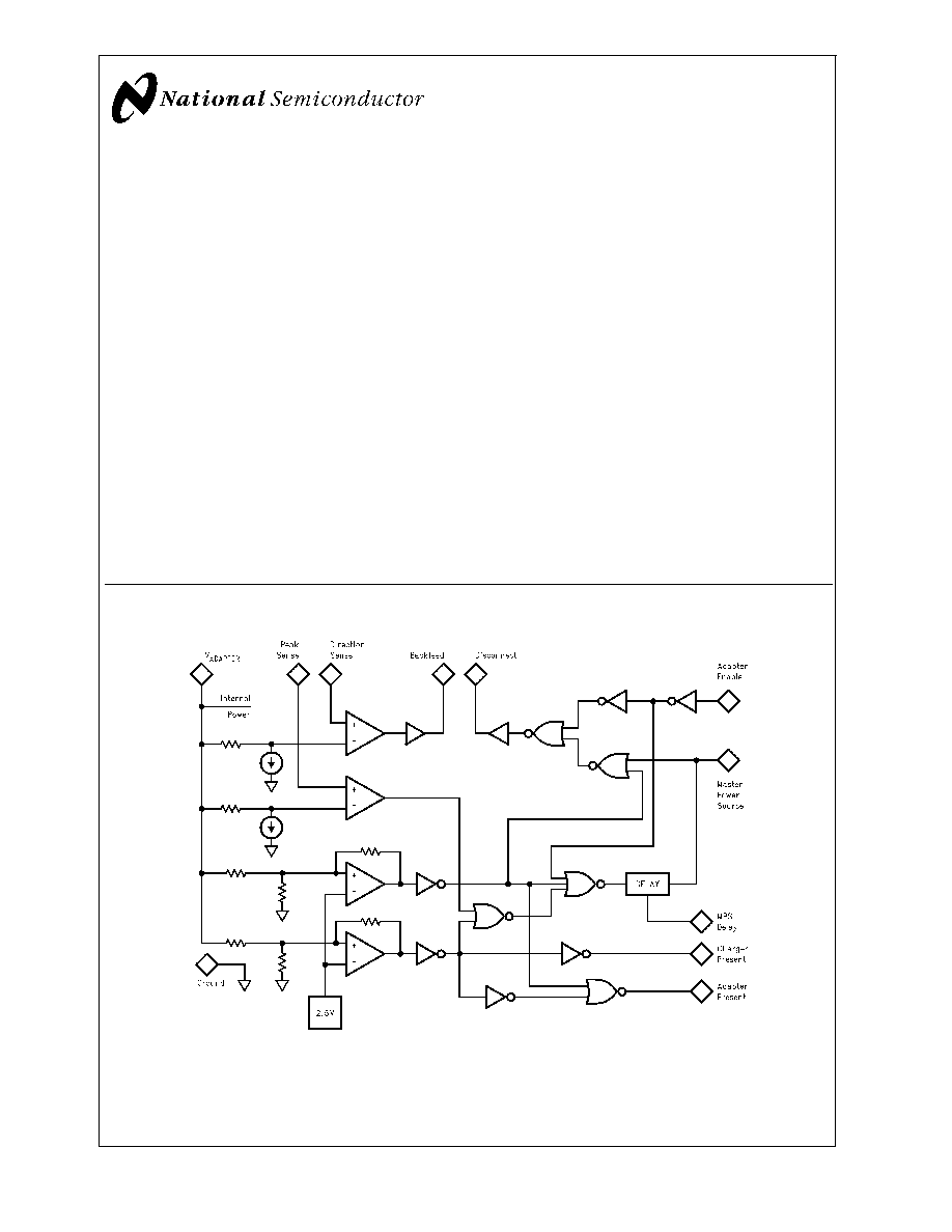
Block Diagram
10130901
April 2001
LM2601
Adapter
Interface
Circuit
� 2001 National Semiconductor Corporation
DS101309
www.national.com
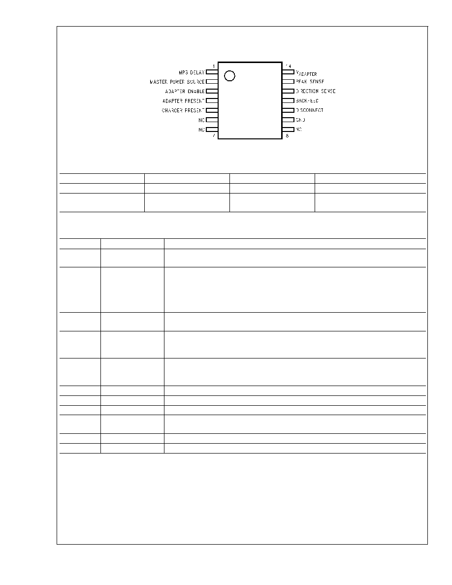
Pin Configuration
TSSOP-14
10130902
Ordering Information
Order Number
Package Number
Package Type
Supplied As
*
LM2601MTC
MTC14
TSSOP-14
Rail (94 Units/Rail)
LM2601MTCX
MTC14
TSSOP-14
Tape and Reel (2500
Units/Reel)
*
Partial Rails are available, there is no minimum order quantity. Tape and Reel is supplied as full reels only.
Pin Description
Pin No.
Name
Function
1
MPS DELAY
A capacitor between this pin and ground sets the delay of the MPS risetime. See MPS
DELAY description in Typical Application section.
2
MASTER POWER
SOURCE
Bi-directional logic pin. If driven high by an external source, indicates that a battery is
powering the power bus. If driven high by the AIC, indicates the adapter is powering the
bus. AIC cannot drive MPS low. If there is no valid adapter voltage present, the pin is not
an output but a high impedance logic input. The input is pulled-down via an internal 40k
resistor.
3
ADAPTER
ENABLE
Logic input pin. Active high. Grants permission to the adapter to drive both the power bus
and the MPS signal.
4
ADAPTER
PRESENT
Logic output pin. High when 12 volts
<
V
ADAPTER
<
17 volts. The output typically has 40k
pull-down resistor. The source current is not internally limited and the part can be
damaged if the output is shorted to ground when driven HIGH.
5
CHARGER
PRESENT
Logic output pin. High when V
ADAPTER
>
17 volts. The output typically has 40k pull-down
resistor. The source current is not internally limited and the part can be damaged if the
output is shorted to ground when driven HIGH.
9
GND
IC ground pin.
10
DISCONNECT
Drives the gate of the disconnect P-ch FET.
11
BACKFEED
Drives the gate of the backfeed P-ch FET.
12
DIRECTION
SENSE
Connection for current sense resistor to control BACKFEED.
13
PEAK SENSE
Connection for current sense resistor to control DISCONNECT.
14
V
ADAPTER
Power input pin. Output of AC adapter, auto adapter or airline adapter.
LM2601
www.national.com
2

Absolute Maximum Ratings
(Note 1)
If Military/Aerospace specified devices are required,
please contact the National Semiconductor Sales Office/
Distributors for availability and specifications.
V
ADAPTER
-0.3V to 28V
V
PEAK SENSE
, V
DIRECTION SENSE
,
V
BACKFEED
, V
DISCONNECT
-0.3V to V
ADAPTER
V
ADAPTER ENABLE
,
V
MASTER POWER SOURCE
-0.3V to 5.5V
V
MPS DELAY
-0.3V to 2V
Storage Temperature
-40�C to 125�C
ESD Ratings
Human Body Model (Note 2)
Machine Model (Note 3)
2kV
200V
Operating Ratings
(Note 1)
Supply Voltage (V
ADAPTER
)
5V to 24V
Ambient Temp. Range
-20�C to 70�C
Junction Temp. Range
-20�C to 85�C
Electrical Characteristics
Limits with standard typeface apply for T
J
= 25�C, and limits in boldface type apply over the full temperature range (Note 4)
Symbol
Parameter
Conditions
Min
Typ
Max
Units
V
AE
Adapter Enable -
3V- or 5V-CMOS or TTL Logic Input
High
Low
2.0
0.8
V
V
AP, CP
Logic Output Voltage
Adapter present, Charger present
High
Low, I
SINK
= 5�A
2.9
3.1
0.25
0.6
V
V
MPSI
Master Power Source
5V-CMOS Logic Input
High
Low
4.0
0.8
V
V
MPSO
Logic Output Voltage
Master Power Source
V
ADAPTER
>
5.8V
High
Low
4.5
4.75
0.05
0.5
V
V
ADAPTER
Adapter Voltage for V
AP
Low-to-High
Transition
11.7
12.0
12.3
V
Hysteresis
1.8
2.0
2.2
V
CHARGER
Adapter Voltage for V
CP
Low-to-High Transition
16.5
17.0
17.4
V
Hysteresis
0.08
0.10
0.12
V
BACKFEED
Current Sense Differential Voltage
Threshold for Driving Backfeed FET
Vadapter - Direction sense,
V
ADAPTER
= 5V
4
3
9
17
18
mV
V
DISCONNECT
Current Sense Differential Voltage
Threshold for Driving Disconnect FET
Vadapter - Peak sense,
V
ADAPTER
= 24V
127
125
135
143
145
mV
V
BACKFEED
,
FET Control Voltage
V
ADAPTER
>
11V
High
V
ADAPTER
-
0.5V
V
V
DISCONNECT
V
ADAPTER
>
11V
Low
V
ADAPTER
-
10V or
GND+0.5V,
whichever is
greater
t
DRIVE
Rise/Fall Time of FET Drive
(Note 5)
V
ADAPTER
= 10V
C
Load
= 3000pF
3
6
�S
I
Q
Quiescent Current
V
ADAPTER
= 24V
2
10
mA
I
L,B
,
I
L,D
Leakage Current into Backfeed or
Disconnect
V
ADAPTER
= 0V
V
BACKFEED
, V
DISCONNECT
= 18V
1
15
�A
I
L,AE
Input Current into Adapter Enable
Input
V
AE
= 3.3V,
Backfeed/Disconnect = 18V
50
�A
I
L, MPS
Input Current into MPS Input
V
MPS
= 5.5V
175
�A
TC
DELAY
Delay Time Temperature Coefficient
4000
ppm/�C
Note 1: Absolute Maximum Ratings indicate limits beyond which damage to the device may occur. Operating Ratings indicate conditions for which the device is
intended to be functional, but do not guarantee specific performance limits. For guaranteed specifications and test conditions, see the Electrical Characteristics.
Note 2: The human body model is a 100pF capacitor discharged through a 1.5k
resistor into each pin.
Note 3: The machine model is a 200pF capacitor discharged directly into each pin. All pins are rated for 200V except pins 4 and 5 which are rated for 100V.
Note 4: Datasheet min/max specification limits are guaranteed by design, test, or statistical analysis.
LM2601
www.national.com
3
Electrical Characteristics
(Continued)
Note 5: Adapter Enable input is used to change the state of Disconnect, Direction Sense input is used to change the state of Backfeed.
a.
Fall time is measured as the time it takes Backfeed or Disconnect voltage to go from a high level (approx. V
ADAPTER
- 0.5V) to (V
ADAPTER
- 4V) after the signal
is initiated at Adapter Enable or Direction Sense.
b.
Rise time is measured as the time it takes Backfeed or Disconnect voltage to go from a low level (approx. 0.5V) to (V
ADAPTER
- 2V) after the signal is initiated
at Adapter Enable or Direction Sense.
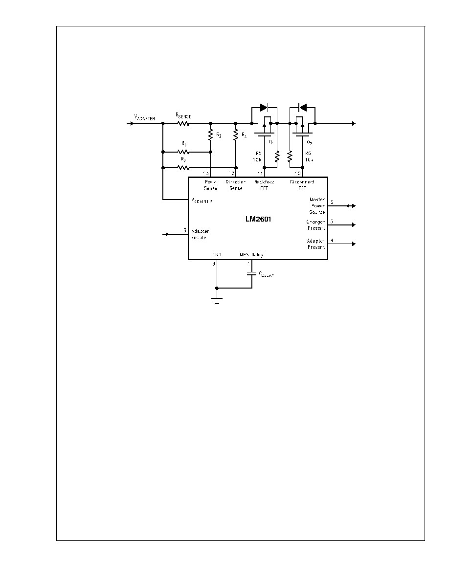
Typical Application
10130903
Notes
1.
R
SENSE
value should be selected to guarantee that a
programmed over current will cause a voltage drop
across R
SENSE
of approx. 135mV. If a higher value of
R
SENSE
has to be selected then R1/R3 resistor divider
should be used to scale the voltage drop down.
2.
Internal and external circuits associated with Direction
Sense and Backfeed FET pins allow to emulate a Schot-
tky diode functionality with much lower forward voltage
drop and, therefore, with much lower power dissipation.
R2/R4 resistor divider programs the backfeed current
protection threshold. The backfeed FET Q1 turns off
when the backfeed current pulse level causes more than
9 mV (typical value) voltage drop between V
adapter
pin
and Direction Sense pin.
3.
Voltage difference (V
DIRECTION SENSE
- V
ADAPTER
) must
be higher than 20mV to reliably isolate the adapter in
case of leakage.
4.
R5 and R6 prevent the FETs from turning on unless
driven by LM2601.
5.
C
DELAY
value can be calculated from the following for-
mula:
C
DELAY
(nF) = T
DELAY
(�s)/90 at 25�C
6.
T
DELAY
temperature coefficient equals 4000ppm/�C. See
also the Typical Delay Time vs. Temperature graph.
7.
Pin Master Power Source (MPS) should be connected to
System Management Controller's (SMC) and battery
packs' GPIOs. When SMC detects a powered AC
adapter via active signals at Charger Present or Adapter
Present outputs, it asserts Adapter Enable signal and
isolates the battery pack(s). Adapter Enable signal turns
the Disconnect FET on. When the AC adapter is un-
plugged or powered off, SMC enables one of the system
battery packs. The battery packs' embedded controller
starts driving the logic MPS signal high that turns the
Disconnect FET off.
LM2601
www.national.com
4
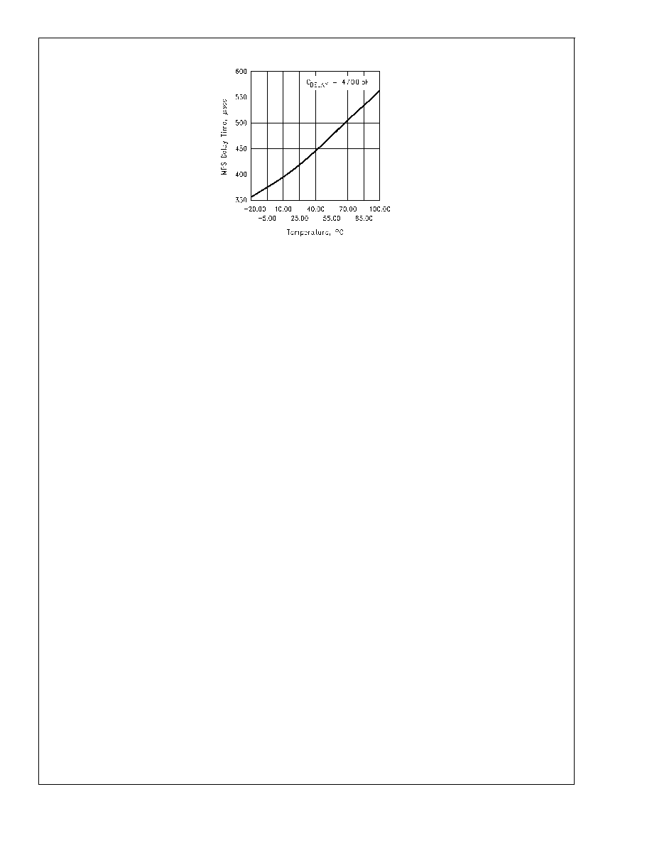
Typical Delay Time vs. Temperature
10130905
Application Information
The adapter interface circuit (AIC) IC provides the control
functions necessary for use in mating a constant voltage
output AC-DC adapter or airline adapter to a notebook com-
puter system or a portable device. It allows optimal battery
charging during computer operation, and allows battery dis-
charge for battery gas gauge calibration. It receives control
signals from the notebook computer, monitors input current
from the adapter, provides adapter voltage status to the
notebook system management microcontroller (or
embed-
ded controller
), and appropriately drives MOSFET switches
to electrically connect the adapter to the computer.
AIC will allow a system designer to solve various power
management tasks typical for an adapter powered systems
containing a rechargeable battery.
When a notebook computer is being powered from a battery
and the adapter is plugged in, the computer should start
drawing power from the adapter, not from the battery. The
most time efficient charging scenario is when a computer
draws the full rated current from a constant voltage adapter.
The computer uses what it needs to run, and passes all
remaining power on to the battery for charging. The com-
puter should be able to automatically refuse to charge a
battery when powered from an airplane power line. It may be
necessary sometimes to have a computer fully discharging
the battery and then fully recharging it (for battery gas gauge
calibration purposes) while being powered by an AC adapter.
AIC will also allow a computer to prevent backfeeding cur-
rent into an adapter if the adapter is not powered while being
plugged into the computer (some of existing adapters can
draw current from the computer under this conditions for
charging the AC adapter output bulk capacitance from the
computer battery).
While the lowest usable adapter voltage is about 9.5V, that is
V
ADAPTER
= 11.7V minus 2.2V hysteresis, AIC is operational
down to V
ADAPTER
= 5V. This means that AIC will not gen-
erate false readings down to V
ADAPTER
= 5V. Such false
readings would be MPS = HIGH, ADAPTER PRESENT =
HIGH, CHARGER PRESENT = HIGH.
AIC determines usable voltage ranges by comparing
V
ADAPTER
with an internal 2.5V voltage reference (see also
Electrical Characteristics). AIC detects operating current limit
and leakage current limit into the adapter jack by differential
sensing across current sense resistor R
SENSE
either directly
or scaled down by resistor dividers R1/R3 and R2/R4.
When designing the LM2601 into a system it may be neces-
sary to consider ESD protection requirements for the
adapter jack according to your system design spec.
LM2601
www.national.com
5