
LM2608
400mA Sub-miniature, High Efficiency, Programmable
DC-DC Converter with Linear Mode
General Description
The LM2608 step-down DC-DC converter is optimized for
powering ultra-low voltage circuits from a single Lithium-Ion
cell. It provides up to 400mA over an input voltage range of
2.8V to 5.5V. Operating from a 1.35V reference, this device
provides
pin-selectable
output
voltages
of
1.3V/1.5V
(300mA) for low voltage version or 1.5V/1.8V (400mA) for
high voltage version. This allows adjustment for DSP or CPU
voltage options, as well as dynamic output voltage switching
for reduced power consumption. Internal synchronous recti-
fication provides high efficiency.
The LM2608 offers superior features and performance for
mobile phones and similar portable applications with com-
plex power management systems. Pin-selectable PWM low-
noise and linear micropower modes offer improved system
control for maximizing battery life. During full power opera-
tion, fixed-frequency PWM mode reduces interference in RF
and data acquisition applications by minimizing noise har-
monics at sensitive IF and sampling frequencies. A SYNC
input allows synchronizing the switching frequency in a
range of 500kHz to 1MHz to avoid noise from intermodula-
tion with system frequencies. Linear operation reduces qui-
escent current to 20µA (typ) during system standby for ex-
tended battery life. It provides up to 3 mA in the linear mode.
Shutdown reduces battery consumption to 0.02µA (typ.).
The LM2608 is available in a 10 pin Micro SMD package.
This package uses National's wafer level chip-scale Micro
SMD technology and offers the smallest possible size. A high
switching frequency (600KHz) allows use of tiny surface-
mount components. Only four small external surface-mount
components, an inductor and three ceramic capacitors are
required. Pin selectable output voltage eliminates the need
for bulky external feedback resistors.
Key Specifications
n
Operates from a single LiION cell (2.8V to 5.5V)
n
Pin selectable output voltage (1.5V/1.8V or 1.3V/1.5V
versions), without external feedback resistors
n
400mA maximum load capability
n
±
1% PWM mode DC output voltage precision
(Excluding external reference tolerance)
n
5mV typ PWM mode output voltage ripple
n
20 µA typ quiescent current (Linear Mode)
n
0.02µA typ shutdown mode current
n
Internal synchronous rectification for high efficiency
(91% at 2.8V
IN
, 1.8V
OUT
)
n
600kHz PWM mode switching frequency
n
SYNC input for PWM mode frequency synchronization
from 500kHz to 1MHz
n
15% accuracy for F
OSC
and I
lim
Features
n
Sub-miniature 10-pin thin Micro SMD package
n
Only four tiny surface-mount external components
required
n
Uses small ceramic capacitors
n
Internal soft start
n
Current and Thermal shutdown protection
n
No external compensation required
Applications
n
Mobile Phones
n
Hand-Held Radios
n
Battery Powered Devices
Typical Application Circuit
20036602
December 2002
LM2608
400mA
Sub-miniature,
High
Efficiency
,
Programmable
DC-DC
Converter
with
Linear
Mode
© 2003 National Semiconductor Corporation
DS200366
www.national.com
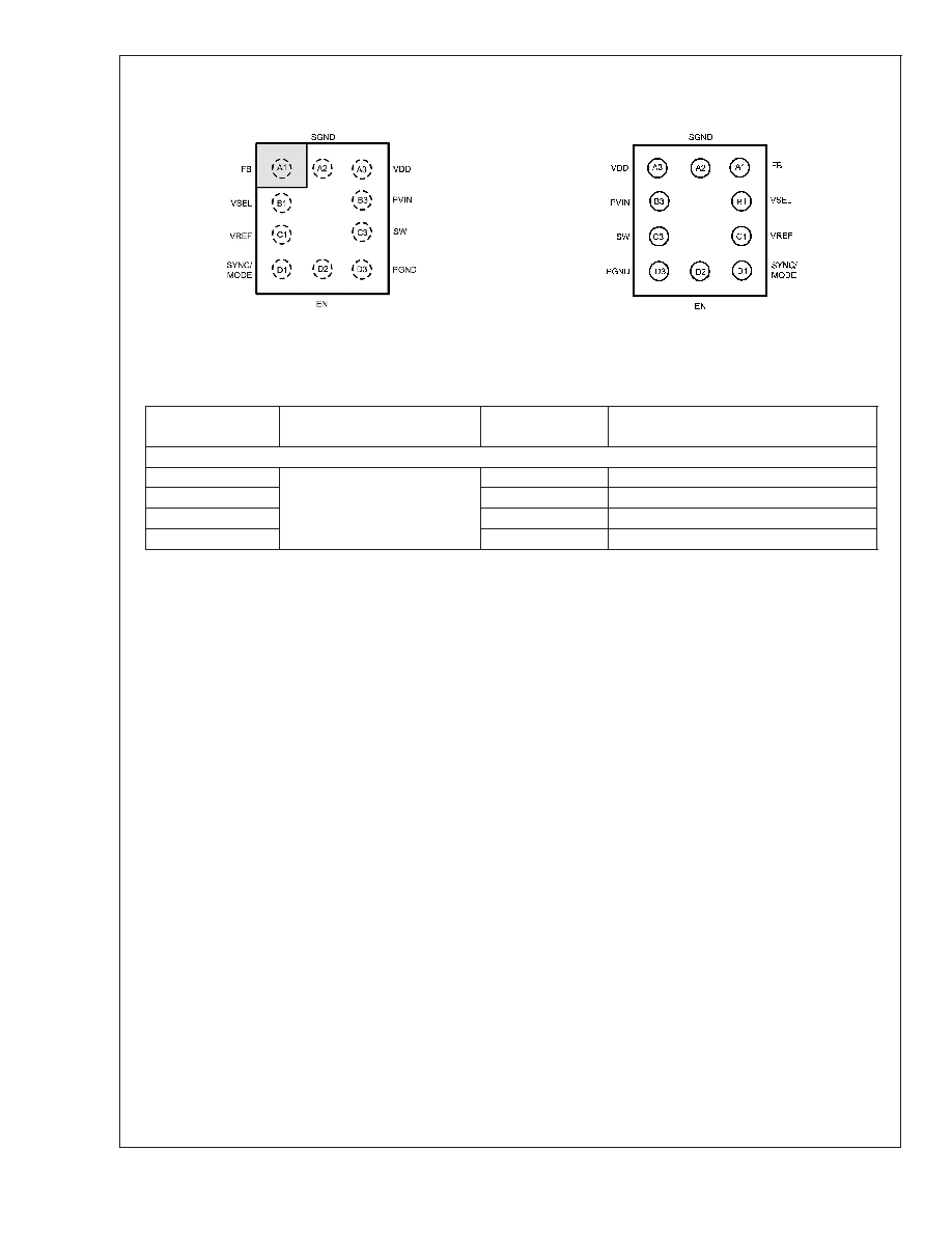
Connection Diagrams
Micro SMD package
20036604
TOP VIEW
20036605
BOTTOM VIEW
Ordering Information
Order Number
Package Type
NSC Package
Marking (*)
Supplied As
10-Pin Micro SMD
LM2608ATL-1.3
10-bump Wafer Level Chip Scale
(Micro SMD)
XYTT IS43A
250 Units, Tape and Reel
LM2608ATL-1.8
XYTT IS44A
250 Units, Tape and Reel
LM2608ATLX-1.3
XYTT IS43A
3000 Units, Tape and Reel
LM2608ATLX-1.8
XYTT IS44A
3000 Units, Tape and Reel
(*) XY - denotes the date code marking (2 digit) in production
(*) TT - refers to die run/lot traceability for production
(*) I - pin one indication
(*) S - product line designator
Note the Package Marking may change over the course of production
LM2608
www.national.com
2

Pin Description
Pin Number (*)
Pin Name
Function
A1
FB
Feedback Analog Input. Connect to the output at the output filter capacitor (Figure 1)
B1
VSEL
Output Voltage Selection Input. Set this digital input to:
VDD for 1.8V output voltage (1.5V for LM2608ATL-1.3)
SGND for 1.5V output voltage (1.3V for LM2608ATL-1.3)
C1
VREF
External Reference Input. Drive this analog input with a 1.35V reference to set the output
voltage. The LM2608 uses an internal reference while in LDO mode. (see Note 5 in the
Electrical Characteristics table for further information.)
D1
SYNC/MODE
Synchronization Input. Use this digital input for frequency synchronization or mode control.
Set:
SYNC/MODE = high for low-noise 600kHz PWM mode
SYNC/MODE = low for low-current LDO mode
SYNC/MODE = 500kHz - 1MHz external clock for synchronization to an external clock in
PWM mode. See Synchronization and Operating Modes in the Device Information section.
D2
EN
Enable Input. Set this Schmitt trigger digital input high for normal operation.
D3
PGND
Power Ground
C3
SW
Switching Node connection to the internal PFET switch and NFET synchronous rectifier.
Connect to an inductor with a saturation current rating that exceeds the max. Switch Peak
Current Limit specification of the LM2608 (Figure 1)
B3
PVIN
Power Supply Input to the internal PFET switch. Connect to the input filter capacitor
(Figure 1).
A3
VDD
Analog Supply Input. If board layout is not optimum, an optional 0.1µF ceramic capacitor
is suggested (Figure 1)
A2
SGND
Analog and Control Ground
(*) Note that the pin numbering scheme for the Micro SMD package was revised in April,2002 to conform to JEDEC standard. Only the pin numbers were revised.
No changes to the physical location of the inputs/outputs were made. For reference purpose, the obsolete numbering had FB as pin 1, VSEL as pin 2, VREF as pin
3, SYNC as pin 4, EN as pin 5, PGND as pin 6, SW as pin 7, PVIN as pin 8, VDD as pin 9 and SGND as pin 10.
LM2608
www.national.com
3

Absolute Maximum Ratings
(Note 1)
If Military/Aerospace specified devices are required,
please contact the National Semiconductor Sales Office/
Distributors for availability and specifications.
PVIN, VDD, to SGND
-0.2V to +6V
PGND to SGND
-0.2V to +0.2V
EN, SYNC/MODE, VSEL to SGND
-0.2V to +6V
FB, SW
(GND -0.2V) to
(VDD +0.2V)
Storage Temperature Range
-45∞C to +150∞C
Lead temperature
(Soldering, 10 sec.)
260∞C
Junction Temperature (Note 2)
-25∞C to 125∞C
Minimum ESD Rating
Human body model, C = 100pF, R =
1.5 k
±
2.0kV
Thermal Resistance (
JA
)
LM2608ATL(Note 3)
140∞C/W
Electrical Characteristics
Specifications with standard typeface are for T
A
= T
J
= 25∞C, and those in bold face type apply over the full Operating Tem-
perature Range (T
A
= T
J
= -25∞C to +85∞C). Unless otherwise specified, PVIN = VDD = EN = SYNC = 3.6V, VSEL = 0V,
VREF = 1.35V.
Symbol
Parameter
Conditions
Min
Typ
Max
Units
V
IN
Input Voltage Range (Note
4)
PVIN = VDD, VSEL = V
IN
2.8
5.5
V
V
FB
Feedback Voltage
PWM Mode
SYNC/MODE = V
IN
(Note 5)
LM2608ATL-1.3, VSEL = 0V
1.287
1.30
1.313
V
LM2608ATL-1.3, VSEL = V
IN
1.485
1.50
1.515
LM2608ATL-1.8, VSEL = 0V
1.485
1.50
1.515
LM2608ATL-1.8, VSEL = V
IN
1.782
1.80
1.818
V
FB, LIN
Feedback Voltage
LIN Mode
(SYNC/MODE =0V)
V
IN
= 3.6V
I
OUT
= 100µA
LM2608ATL-1.3, VSEL = 0V
1.261
1.30
1.339
V
LM2608ATL-1.3, VSEL = V
IN
1.455
1.50
1.545
LM2608ATL-1.8, VSEL = 0
1.455
1.50
1.545
LM2608ATL-1.8, VSEL = V
IN
1.746
1.80
1.854
V
OUT_LDO
Line Regulation
I
OUT
= 100µA
0.1
%/V
Load Regulation
V
IN
= 3.6V, I
OUT
= 10µA to
1.5mA
1.0
%/mA
V
HYST
OVP Comparator Hysteresis
Voltage
(Note 6)
PWM Mode
45
75
mV
I
SHDN
Shutdown Supply Current
EN = 0V
0.02
3
µA
I
Q, PWM
DC Bias Current into VDD
(PWM Mode)
FB = 2V
SYNC/MODE =V
IN
590
725
µA
I
Q, LIN
DC Bias Current into VDD
(LDO Mode)
SYNC/MODE = 0V,
I
OUT
= 0 mA
20
30
R
DSON (P)
Pin-Pin Resistance for P
FET
370
500
m
R
DSON (N)
Pin-Pin Resistance for N
FET
330
500
m
R
DSON , TC
FET Resistance
Temperature Coefficient
0.5
%/C
I
SC, LDO
Short Circuit (LDO)
V
OUT
= GND
SYNC/MODE = 0V
3
6
8
mA
I
lim
Switch Peak Current Limit
(Note 7)
LM2608ATL-1.3
383
460
518
mA
LM2608ATL-1.8
510
620
690
V
EN_H
EN Positive Going
Threshold Voltage
(Note 8)
0.80
1.3
V
V
EN_L
EN Negative Going
Threshold Voltage
(Note 8)
0.4
0.75
V
LM2608
www.national.com
4

Electrical Characteristics
(Continued)
Specifications with standard typeface are for T
A
= T
J
= 25∞C, and those in bold face type apply over the full Operating Tem-
perature Range (T
A
= T
J
= -25∞C to +85∞C). Unless otherwise specified, PVIN = VDD = EN = SYNC = 3.6V, VSEL = 0V,
VREF = 1.35V.
Symbol
Parameter
Conditions
Min
Typ
Max
Units
V
SYNC_H
SYNC/MODE Positive
Going Threshold Voltage
0.85
1.3
V
V
SYNC_L
SYNC/MODE Negative
Going Threshold Voltage
0.4
0.80
V
V
SEL_H
V
SEL
Positive Going
Threshold Voltage
0.80
1.3
V
V
SEL_L
V
SEL
Negative Going
Threshold Voltage
0.4
0.75
V
I
SEL
VSEL Pull Down Current
VSEL = 1.2V
0.70
2
µA
I
REF
Input current into VREF pin
15
150
nA
f
sync
SYNC/MODE Clock
Frequency Range
(Note 9)
500
1000
kHz
F
OSC
Internal Oscillator
Frequency
LM2608ATL-1.3/1.8, PWM
Mode
510
610
690
kHz
T
min
Minimum ON-Time of P FET
Switch in PWM Mode
200
ns
Note 1: Absolute Maximum Ratings indicate limits beyond which damage to the device may occur. Operating Ratings are conditions for which the device is intended
to be functional, but parameter specifications may not be guaranteed. For guaranteed specifications and associated test conditions, see the Min and Max limits and
Conditions in the Electrical Characteristics table. Electrical Characteristics table limits are guaranteed by production testing, design or correlation using standard
Statistical Quality Control methods. Typical (Typ) specifications are mean or average values from characterization at 25∞C and are not guaranteed.
Note 2: Thermal shutdown will occur if the junction temperature exceeds the 150∞C maximum junction temperature of the device.
Note 3: Thermal resistance specified with 2 layer PCB(0.5/0.5 oz. cu).
Note 4: The LM2608 is designed for cell phone applications where turn-on after system power-up is controlled by the system processor and internal UVLO (Under
Voltage LockOut) circuitry is unnecessary. The LM2608 has no UVLO circuitry and should be kept in shutdown by holding the EN pin low until the input voltage
exceeds 2.8V. Although the LM2608 exhibits safe behavior while enabled at low input voltages, this is not guaranteed.
Note 5: The LM2608 PWM mode output voltage precision is
±
1% when operating from an external 1.35V reference voltage.
Note 6: The hysteresis voltage is the minimum voltage swing on FB that causes the internal feedback and control circuitry to turn the internal PFET switch on and
then off, during test mode.
Note 7: Current limit is built-in, fixed, and not adjustable. If the current limit is reached while the output is pulled below about 0.7V, the internal PFET switch turns
off for 2.5 µs to allow the inductor current to diminish.
Note 8: EN is a Schmitt trigger digital input with logic thresholds that are independent of supply voltage at the VDD pin.
Note 9: SYNC driven with an external clock switching between VDD and GND. When an external clock is present at SYNC, the IC is forced into PWM mode at the
external clock frequency. The LM2608 synchronizes to the rising edge of the external clock.
LM2608
www.national.com
5