 | –≠–ª–µ–∫—Ç—Ä–æ–Ω–Ω—ã–π –∫–æ–º–ø–æ–Ω–µ–Ω—Ç: LM2623EV | –°–∫–∞—á–∞—Ç—å:  PDF PDF  ZIP ZIP |
LM2623
General Purpose, Gated Oscillator Based, DC/DC Boost
Converter
General Description
The LM2623 is a high efficiency, general purpose, step-up
DC-DC switching regulator for battery-powered and low in-
put voltage systems. It accepts an input voltage between .8
and 14 volts and converts it into a regulated output voltage
between 1.24 and 14 volts. Efficiencies up to 90% are
achievable with the LM2623.
In order to adapt to a number of applications, the LM2623
allows the designer to vary the output voltage, the operating
frequency (300kHz to 2 MHz) and duty cycle (17% to 90%)
to optimize the part's performance. The selected values can
be fixed or can vary with battery voltage or input to output
voltage ratio. The LM2623 uses a very simple, on/off regu-
lation mode to produce good efficiency and stable operation
over a wide operating range. It normally regulates by skip-
ping switching cycles when it reaches the regulation limit
(Pulse Frequency Modulation).
Note: Please read the "Non-Linear Effect" and "Choosing
The Correct C3 Capacitor" sub-sections of the Design Pro-
cedure section of this data sheet, so that any challenges with
designing with this part can be taken into account before a
board design/layout is finalized.
For Alternative Solutions, See Also: LM2700, LM2622,
LM2731, LM2733, and LM2621.
Features
n
Good Efficiency Over a Very Wide Load Range
n
Very Low Output Voltage Ripple
n
Small, Mini-SO-8 Package (Half the Footprint of
Standard 8 pin SO Package)
n
1.09 mm Package Height
n
Up to 2 MHz Switching Frequency
n
.8V to 14V Operating Voltage
n
1.1V Start-up Voltage
n
1.24V - 14V Adjustable Output Voltage
n
Up to 2A Load Current at low Output Voltages
n
0.17
Internal MOSFET
n
Up to 90% Regulator Efficiency
n
80 µA Typical Operating Current (into V
DD
pin of supply)
n
<
2.5µA Guaranteed Supply Current In Shutdown
n
4mm x 4mm Thermally Enhanced LLP Package Option
Applications
n
Cameras, Pagers and Cell Phones
n
PDAs,Palmtop Computers, GPS devices
n
White LED Drive, TFT or Scanned LCDs
n
Flash Memory Programming
n
Hand-Held Instruments
n
1, 2, 3 or 4 Cell Alkaline Systems
n
1, 2 or 3 Cell Lithium-ion Systems
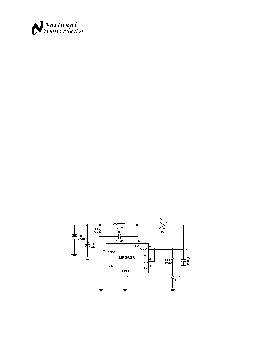
Typical Application Circuit
20038801
July 2003
LM2623
General
Purpose,
Gated
Oscillator
Based,
DC/DC
Boost
Converter
© 2003 National Semiconductor Corporation
DS200388
www.national.com
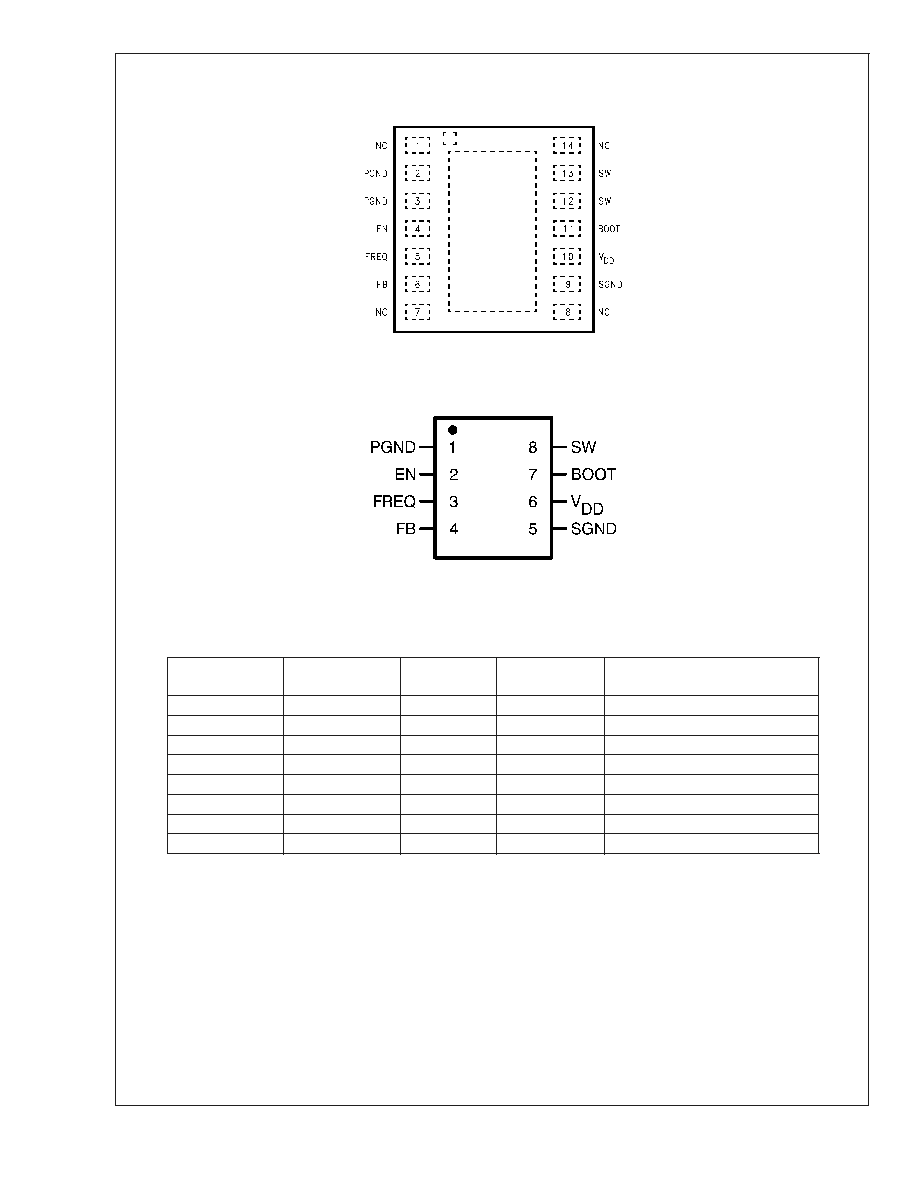
Connection Diagram
LLP Package
20038802
Top View
Mini SO-8 (MM) Package
20038818
Top View
Ordering Information
Order Number
Package Type
NSC Package
Drawing
Package
Marking
Supplied As
LM2623MMX
Mini SO-8
MUA08A
S46B
3000 Units on Tape and Reel
LM2623AMMX
Mini SO-8
MUA08A
S46A
3000 Units on Tape and Reel
LM2623AMM
Mini SO-8
MUA08A
S46A
1000 Units on Tape and Reel
LM2623MM
Mini SO-8
MUA08A
S46B
1000 Units on Tape and Reel
LM2623LDX
LLP-14
LDA14A
2623AB
4500 Units on Tape and Reel
LM2623ALDX
LLP-14
LDA14A
2623A
4500 Units on Tape and Reel
LM2623LD
LLP-14
LDA14A
2623AB
1000 Units on Tape and Reel
LM2623ALD
LLP-14
LDA14A
2623A
1000 Units on Tape and Reel
LM2623
www.national.com
2

Pin Description
LLP-14 Pin
MSOP-8 Pin
Name
Function
1
NC
No Connect
2, 3
1
PGND
Power Ground (LLP Pins 2 & 3 must be shorted
together).
4
2
EN
Active-Low Shutdown Input
5
3
FREQ
Frequency Adjust. An external resistor connected
between this pin and a voltage source sets the
switching frequency of the LM2623.
6
4
FB
Output Voltage Feedback
7
NC
No Connect
8
NC
No connect
9
5
SGND
Signal Ground
10
6
V
DD
Power Supply for Internal Circuitry
11
7
BOOT
Bootstrap Supply for the Gate Drive of Internal
MOSFET Power Switch
12, 13
8
SW
Drain of the Internal MOSFET Power Switch. (LLP Pins
12 & 13 must be shorted together).
14
NC
No Connect
DAP
DAP
To be soldered to board for enhanced thermal
dissipation. To be electrically isolated/floating.
LM2623
www.national.com
3
Absolute Maximum Ratings
(Note 1)
If Military/Aerospace specified devices are required,
please contact the National Semiconductor Sales Office/
Distributors for availability and specifications.
SW Pin Voltage
-0.5 V to 14.5V
BOOT, V
DD
, EN and FB Pins
-0.5V to 10V
FREQ Pin
100µA
T
Jmax
(Note 2)
150∞C
Storage Temperature Range
-65∞C to +150∞C
Lead Temp. (Soldering, 5 sec)
260∞C
Power Dissipation (T
A
=25∞C)
(Note 2)
500mW
ESD Rating (Note 3)
2kV
Operating Conditions
(Note 1)
V
DD
Pin
3V to 5V
FB, EN Pins
0 to V
DD
BOOT Pin
0 to 10V
Ambient Temperature (T
A
)
-40∞C to +85∞C
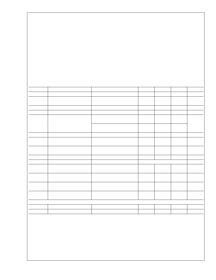
Electrical Characteristics
Limits in standard typeface are for T
J
= 25∞C, and limits in boldface type apply over the full operating temperature range of
-40∞C to +85∞C. Unless otherwise specified: V
DD
= V
OUT
= 3.3V.
Symbol
Parameter
Condition
Typ
Min
Max
Units
V
DD_ST
Start-Up Supply Voltage 25∞C
I
LOAD
= 0mA (Note 4)
1.1
V
V
IN_OP
Minimum Operating Supply
Voltage (once started)
I
LOAD
= 0mA
0.65
.8
V
V
FB
FB Pin Voltage
1.24
1.2028
1.2772
V
V
OUT_MAX
Maximum Output Voltage
14
V
Efficiency
V
IN
= 3.6V; V
OUT
= 5V; I
LOAD
=
500mA
87
%
V
IN
= 2.5V; V
OUT
= 3.3V; I
LOAD
= 200mA
87
D
Switch Duty Cycle
17
%
I
DD
Operating Quiescent Current
(Note 5)
FB Pin
>
1.3V; EN Pin at V
DD
80
110
µA
I
SD
Shutdown Quiescent Current
(Note 6)
V
DD
, BOOT and SW Pins at
5.0V; EN Pin
<
200mV
0.01
2.5
µA
I
CL
Switch Peak Current Limit
LM2623A
2. 85
2.2
A
I
C
Switch Peak Current Limit
LM2623
1.2
A
R
DS_ON
MOSFET Switch On
Resistance
0.17
0.26
JA
Thermal Resistance
MM Package, Junction to
Ambient(Note 2)
240
∞C/W
JA
Thermal Resistance
LLP Package, Junction to
Ambient(Notes 2, 8)
40
∞C/W
JA
Thermal Resistance
LLP Package, Junction to
Ambient(Notes 2, 9)
56
∞C/W
Enable Section
V
EN_LO
EN Pin Voltage Low (Note 7)
0.15V
DD
V
V
EN_HI
EN Pin Voltage High (Note 7)
0.7V
DD
V
Note 1: Absolute maximum ratings indicate limits beyond which damage to the device may occur. Electrical specifications do not apply when operating the device
outside of its rated operating conditions.
Note 2: The maximum power dissipation must be derated at elevated temperatures and is dictated by T
jmax
(maximum junction temperature),
JA
(junction to
ambient thermal resistance), and T
A
(ambient temperature). The maximum allowable power dissipation at any temperature is P
dmax
= (T
jmax
- T
A
)/
JA
or the number
given in the Absolute Maximum Ratings, whichever is lower.
Note 3: The human body model is a 100 pF capacitor discharged through a 1.5 k
resistor into each pin. For Pin 8 (SW) the ESD rating is 1.0 kV.
Note 4: V
DD
tied to Boot and EN pins. Frequency pin tied to V
DD
through 121K resistor. V
DD_ST
= V
DD
when startu-up occurs. V
IN
is V
DD
+ D1 voltage (usually
10-50 mv at start-up)
Note 5: This is the current into the V
DD
pin.
Note 6: This is the total current into pins V
DD
, BOOT, SW and FREQ.
Note 7: When the EN pin is below V
EN_LO
, the regulator is shut down; when it is above V
EN_HI
, the regulator is operating.
LM2623
www.national.com
4

Electrical Characteristics
(Continued)
Note 8: Junction to ambient thermal resistance (
JA
) is taken from a thermal modeling result, performed under the conditions and guidelines set forthe in the JEDEC
standard JESD51-17. The test board is a 4 layer FR-4 board measuring 102mm x 76mm x 1.6mm with a 3 x 2 array of thermal vias. The ground plane on the board
is 50mm x 50 mm. Thickness of copper layers are 36mm/18mm/18mm/36mm (1.5oz/10z/1oz/1.5ox). Ambient temperature in simulation is 22∞C, still air. Power
dissipation is 1W. (The DAP is soldered.) Fore more information on LLP thermal topics, as well as LLP mounting and soldering specifications please refer to
Application Note 1187: Leadless Leadframe Package (LLP).
Note 9: Exposed DAP soldered to an exposed 1sq. inch area of 1 oz. copper. Thermal resistance can be decreased by using more copper are to dissipate heat.
LM2623
www.national.com
5