 | –≠–ª–µ–∫—Ç—Ä–æ–Ω–Ω—ã–π –∫–æ–º–ø–æ–Ω–µ–Ω—Ç: LM2635M | –°–∫–∞—á–∞—Ç—å:  PDF PDF  ZIP ZIP |
LM2635 5-Bit Programmable
Synchronous Buck Regulator Controller
General Description
The LM2635 is a high speed controller designed specifically
for use in synchronous DC/DC buck converters for the
Pentium
TM
II or Deschutes microprocessor. A 5-bit DAC ac-
cepts the VID code directly from the CPU and adjusts the
output voltage from 1.8V to 3.5V. It provides the power good,
over-voltage protection, and output enable features as re-
quired by Intel VRM specifications. Current limiting is
achieved by monitoring the voltage drop across the r
DS_ON
of the high side MOSFET, which eliminates an expensive
current sense resistor.
The LM2635 employs a fixed-frequency voltage mode PWM
architecture. To provide a faster response to a large and fast
load transient, two ultra-fast comparators are built in to moni-
tor the output voltage and override the primary control loop
when necessary. The PWM frequency is adjustable from 50
kHz to 1 MHz through an external resistor. The wide range of
PWM frequency gives the power supply designer the flexibil-
ity to make trade-offs between load transient response per-
formance, MOSFET cost and the overall efficiency. The
adaptive non-overlapping MOSFET gate drivers help avoid
any potential shoot-through problem while maintaining high
efficiency. BiCMOS gate drivers with rail-to-rail swing ensure
that no spurious turn-on occur. When only 5V is available, a
bootstrap structure can be employed to accommodate an
NMOS high side switch. The precision reference trimmed to
2% over temperature is available externally for use by other
regulators. Dynamic positioning of load voltage, which helps
cut the number of output capacitors, can also be imple-
mented easily.
Features
n
1.8V to 3.5V 5-bit programmable output voltage
n
Synchronous rectification
n
Power Good flag and output enable
n
Over-voltage protection
n
Initial Output Accuracy: 2% over temperature
n
Current limit without external sense resistor
n
Adaptive non-overlapping MOSFET gate drives
n
Adjustable switching frequency: 50 kHz to 1 MHz
n
Dynamic output voltage positioning
n
1.256V reference voltage available externally
n
Plastic SO-20 package
Applications
n
Motherboard power supply/VRM for Cyrix Gxm, Cyrix
Gxi, Cyrix MII, Pentium II, Deschutes, Pentium Pro,
6x86 and K6 processors
n
5V to 1.8V≠3.5V high current power supplies
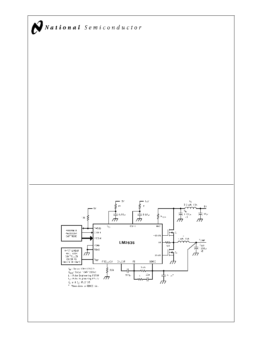
Typical Application
Pentium
TM
is a trademark of Intel Corporation.
DS100119-1
FIGURE 1. 5V to 1.8V≠3.5V, 14A Power Supply
May 2000
LM2635
5-Bit
Programmable
Synchronous
Buck
Regulator
Controller
© 2000 National Semiconductor Corporation
DS100119
www.national.com
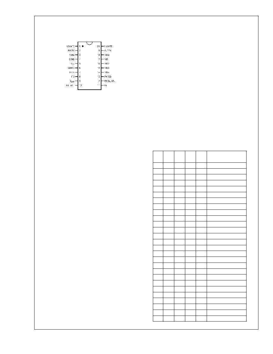
Connection Diagram
Pin Descriptions
LSGATE (Pin 1): Gate drive for the low-side N-channel
MOSFET. This signal is interlocked with HSGATE (Pin 20) to
avoid a shoot-through problem.
BOOTV (Pin 2): Power supply for high-side N-channel
MOSFET gate drive. The voltage should be at least one gate
threshold above the converter input voltage to properly oper-
ate the high-side N-FET.
PGND (Pin 3): Ground for high current circuitry. It should be
connected to system ground.
SGND (Pin 4): Ground for signal level circuitry. It should be
connected to system ground.
V
CC
(Pin 5): Power supply for the controller.
SENSE (Pin 6): Converter output voltage sensing. It pro-
vides input for power good, fast dual comparator control
loop, and over-voltage protection circuitry. It is recom-
mended that a 0.1 µF capacitor be connected between this
pin and ground to avoid potential noise problems.
IMAX (Pin 7): Current limit threshold setting. It sinks a fixed
180 µA current. By connecting a resistor between the high
side MOSFET drain and this pin, a fixed voltage drop can be
built across the resistor. This voltage drop is compared with
the V
DS
of the high-side N-MOSFET to determine if an over-
current condition has occurred.
IFB (Pin 8): High-side N-MOSFET source voltage sensing.
This pin is one V
DS
below drain voltage. When this voltage is
lower than that of IMAX pin during the time the high-side FET
is on, it means V
DS
is higher than the preset voltage across
the IMAX resistor, which can be interpreted as an over-
current condition.
V
REF
(Pin 9): Bandgap reference voltage. This voltage is
mainly for use by other power supplies on the motherboard
which need a reference.
EA_OUT (Pin 10): Output of the error amplifier. The voltage
level on this pin is compared with an internally generated
ramp signal to determine the duty cycle. This pin is neces-
sary for compensating the primary control loop.
FB (Pin 11): Inverting input of the error amplifier. A pin nec-
essary for compensating the control loop.
FREQ_ADJ (Pin 12): Switching frequency adjustment.
Switching frequency can be adjusted by changing the
grounding resistance on this pin.
PWRGD (Pin 13): Power Good. There are two windows
around the DAC output voltage that are associated with
PWRGD pin, the
±
10% window and the
±
8% window. If
PWRGD is initially high (open drain state) and output voltage
travels out of
±
10% window, PWRGD goes to low (low im-
pedance to ground). If PWRGD is initially low and output
voltage travels into the
±
8% window and has stayed within
the window for at least 10 ms, PWRGD goes to high. A
PWRGD high means the output voltage is at least within the
±
10% window whereas a PWRGD low indicates the output
voltage is definitely outside the
±
8% window.
VID4:0 (Pins 14, 15, 16, 17, 18): Voltage Identification
Code. The five pins accept an open-ground pattern 5-bit bi-
nary code from outside the chip (typically from the CPU) for
generating the desired output voltage. Each VID pin is inter-
nally pulled up to V
CC
via a 90 µA current source.
Table 1
shows the code table.
OUTEN (Pin 19): Output Enable. The output voltage is dis-
abled when this pin is pulled low. It is internally pulled up to
V
CC
via a 90 µA current source.
HSGATE (Pin 20): Gate drive for the high-side N-channel
MOSFET. This signal is interlocked with LSGATE (Pin 1) to
avoid a shoot-through problem.
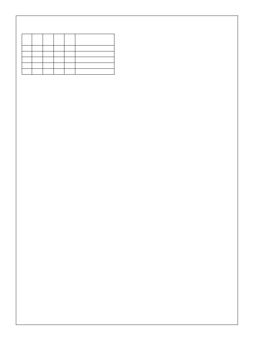
TABLE 1. VID Code and DAC Output
V
ID4
V
ID3
V
ID2
V
ID1
V
ID0
Rated Output
Voltage (V)
0
1
1
1
1
(#) (1.30)
0
1
1
1
0
(#) (1.35)
0
1
1
0
1
(#) (1.40)
0
1
1
0
0
(#) (1.45)
0
1
0
1
1
(#) (1.50)
0
1
0
1
0
(#) (1.55)
0
1
0
0
1
(#) (1.60)
0
1
0
0
0
(#) (1.65)
0
0
1
1
1
(#) (1.70)
0
0
1
1
0
(#) (1.75)
0
0
1
0
1
1.80
0
0
1
0
0
1.85
0
0
0
1
1
1.90
0
0
0
1
0
1.95
0
0
0
0
1
2.00
0
0
0
0
0
2.05
1
1
1
1
1
(shutdown)
1
1
1
1
0
2.1
1
1
1
0
1
2.2
1
1
1
0
0
2.3
1
1
0
1
1
2.4
1
1
0
1
0
2.5
1
1
0
0
1
2.6
1
1
0
0
0
2.7
1
0
1
1
1
2.8
1
0
1
1
0
2.9
1
0
1
0
1
3.0
TOP VIEW
DS100119-3
Plastic SO-20
Order Number LM2635M
See NS Package Number M20B
LM2635
www.national.com
2
Pin Descriptions
(Continued)
TABLE 1. VID Code and DAC Output (Continued)
V
ID4
V
ID3
V
ID2
V
ID1
V
ID0
Rated Output
Voltage (V)
1
0
1
0
0
3.1
1
0
0
1
1
3.2
1
0
0
1
0
3.3
1
0
0
0
1
3.4
1
0
0
0
0
3.5
#: These voltages are disabled, can be enabled upon request.
LM2635
www.national.com
3
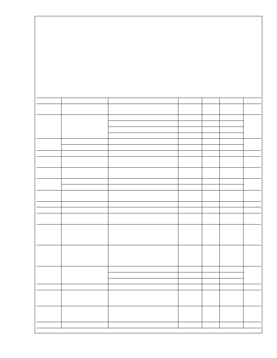
Absolute Maximum Ratings
(Note 1)
If Military/Aerospace specified devices are required,
please contact the National Semiconductor Sales Office/
Distributors for availability and specifications.
(All voltages are referenced to the PGND and SGND pins.)
V
CC
7V
BOOTV
15V
Junction Temperature
150∞C
DC Power Dissipation (Note 2)
1.42W
Storage Temperature
-65∞C to +150∞C
Soldering Time, Temperature
Wave (4 seconds)
Infrared (10 seconds)
Vapor Phase (75 seconds)
260∞C
240∞C
219∞C
ESD Susceptibility (Note 3)
2 kV
Recommended Operating
Conditions
(Note 1)
Supply Voltage Range (V
CC
)
4.5V to 5.5V
Junction Temperature Range
0∞C to +125∞C
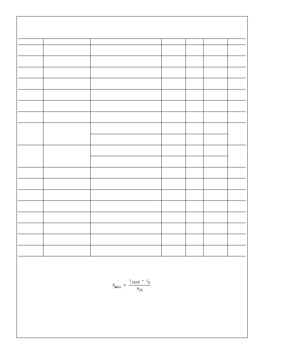
Electrical Characteristics
V
CC
= 5V unless otherwise indicated under the Conditions column. Typicals and limits appearing in plain type apply for T
A
=
T
J
= +25∞C. Limits appearing in boldface type apply over 0∞C to +70∞C.
Symbol
Parameter
Conditions
Min
Typ
Max
Units
V
BOOTV
FET Driver Supply
Voltage
15
V
V
DACOUT
5-Bit DAC Output
Voltage
VID4:0=00101
1.773
1.809
1.845
V
VID4:0=00001
1.969
2.009
2.049
VID4:0=11101
2.165
2.209
2.253
VID4:0=10111
2.753
2.809
2.865
V
OUT
DC Load Regulation
I
OUT
=0 to 14A
Figure 2
-5
mV
DC Line Regulation
V
IN
=4.75V to 5.25V
Figure 2
1
G
EA
Error Amplifier DC Gain
85
dB
SR
EA
Error Amplifier Slew
Rate
6
V/µs
BW
EA
Error Amplifier Unity
Gain Bandwidth
5
MHz
I
Q_VCC
Operating V
CC
Current
OUTEN=V
CC
=5V, VID=10111
1.5
2.5
4
mA
Shutdown V
CC
Current
OUTEN Floating, VID0:4 Floating
1
1.5
3
I
Q_BOOTV
BOOTV Pin Quiescent
Current
BOOTV=12V, OUTEN=0, VID0:4
Floating
4
µA
D
MAX
Maximum Duty Cycle
90
%
D
MIN
Minimum Duty Cycle
0
%
R
SENSE
SENSE Pin Resistance
to Ground
7
11.5
16
k
R
DS_SRC
FET Driver
Drain-Source ON
Resistance when
Sourcing Current
BOOTV=5V
7
R
DS_SINK
FET Driver
Drain-Source ON
Resistance when
Sinking Current
(Independent of BOOTV Voltage)
1.7
f
OSC
Oscillator Frequency
R
FA
= 84 k
250
300
350
kHz
R
FA
= 22 k
1000
R
FA
= 10.5 k
2000
I
MAX
IMAX Pin Sink Current
V
IMAX
= 5V, V
IFB
= 6V, V
CC
= 5V
130
180
230
µA
V
OUTEN_IH
OUTEN Pin Input Logic
Low to Logic High Trip
Point
OUTEN Voltage
3.5
3.0
V
V
OUTEN_IL
OUTEN Pin Input Logic
High to Logic Low Trip
Point
OUTEN Voltage
1.8
1.5
V
V
REF
Band Gap Reference
I
VREF
= 0 mA
1.231
1.256
1.281
V
LM2635
www.national.com
4
Electrical Characteristics
(Continued)
V
CC
= 5V unless otherwise indicated under the Conditions column. Typicals and limits appearing in plain type apply for T
A
=
T
J
= +25∞C. Limits appearing in boldface type apply over 0∞C to +70∞C.
Symbol
Parameter
Conditions
Min
Typ
Max
Units
V
REF_LOAD
Reference Voltage at
Full Load
I
VREF
= 0.5 mA, Sourcing
1.229
1.254
1.279
V
V
REF_525
Reference Voltage at
High Line
I
VREF
= 0 mA, V
CC
= 5.25V
1.232
1.257
1.282
V
V
REF_475
Reference Voltage at
Low Line
I
VREF
= 0 mA, V
CC
= 4.75V
1.230
1.258
1.280
V
V
REF_LOAD
Reference Voltage
Load Regulation
I
VREF
= 0.5 mA, Sourcing
-2
mV
V
REF_LINE
Reference Voltage Line
Regulation
I
VREF
= 0 mA, V
CC
Changes from
5.25V to 4.75V
-0.5
mV
V
SAWL
Ramp Signal Valley
Voltage
1.25
V
V
SAWH
Ramp Signal Peak
Voltage
3.25
V
V
PWRBAD_GD
PWRGD Pin
Trip
Points (see Pin
Description for Pin 13)
% above DAC Output Voltage, when
Output Voltage
10
%
% below DAC Output Voltage, when
Output Voltage
-10
V
PWRGD_BAD
PWRGD Pin
Trip
Points (see Pin
Description for Pin 13)
% above DAC Output Voltage, when
Output Voltage
8
%
% below DAC Output Voltage, when
Output Voltage
-8
V
OVP
Over-voltage Protection
Trip Point
% above DAC Output Voltage
15
%
t
PWRGD
Power Good Response
Time
V
SENSE
Rises from 0V to Rated
V
OUT
2
6
15
µs
t
PWRBAD
Power Not Good
Response Time
V
SENSE
Falls from Rated V
OUT
to 0V
2
6
15
µs
I
OUTEN
OUTEN Pin Internal
Pull-Up Current
60
90
130
µA
V
VID_IH
VID Pins Logic High
Trip Point
3.5
3.0
V
V
VID_IL
VID Pins Logic Low
Trip Point
1.8
1.3
V
I
VID
VID0:4 Internal Pull-Up
Current
60
90
130
µA
t
SS
Soft Start Duration
2048
clock
cycles
Note 1: Absolute Maximum Ratings are limits beyond which damage to the device may occur. Recommended Operating Conditions are conditions under which
the device operates correctly. Recommended Operating Conditions do not imply guaranteed performance limits.
Note 2: Maximum allowable DC power dissipation is a function of the maximum junction temperature, T
JMAX
, the junction-to-ambient thermal resistance,
JA
, and
the ambient temperature, T
A
. The maximum allowable power dissipation at any ambient temperature is calculated using:
The junction-to-ambient thermal resistance,
JA
, for LM2635 in the M20B package is 88∞C/W.
Note 3: All pins are rated for 2 kV, except for the I
MAX
pin (Pin 7) which is rated for 1.5 kV.
LM2635
www.national.com
5