 | ÐлекÑÑоннÑй компоненÑ: LM2645MTD | СкаÑаÑÑ:  PDF PDF  ZIP ZIP |
Äîêóìåíòàöèÿ è îïèñàíèÿ www.docs.chipfind.ru

LM2645
Advanced Two-Phase Switching Controller With Two
Linear Outputs
General Description
The LM2645 is a feature-rich IC that combines two current
mode synchronous buck regulator controllers, an adjustable
linear regulator controller and a fixed 3.3V standby output
rail.
The two switching regulator controllers operate 180° out of
phase. This feature reduces the input ripple RMS current,
thereby significantly reducing the required input capacitance.
The two switching regulator outputs can also be paralleled to
operate as a dual-phase regulator.
The use of synchronous rectification and pulse-skip opera-
tion at light load achieves high efficiency over a wide load
range. Fixed-frequency operation can be obtained by dis-
abling the pulse-skip mode. The switching frequency of the
LM2645 is user selectable between 200 kHz or 300 kHz.
The first switching controller (Channel 1) features a fixed 5V
output, and the second switching controller controller (Chan-
nel 2) features a fixed 3.3V output. Both channels can also
be independently adjusted from 1.3 to 5.5V. The adjustable
linear regulator can be adjusted from 3.3V to 15V. An internal
5V rail is also available externally for driving bootstrap cir-
cuitry. This rail also serves as the input for an internal LDO
that provides the fixed 3.3V/50mA output rail.
Current-mode feedback control assures excellent line and
load regulation and a wide loop bandwidth for excellent
response to fast load transients. Current is sensed across
either the Vds of the top FET or across an external sense
resistor connected in series with the drain of the top FET.
Current limit is independently adjustable for each channel.
The analog soft-start for the switching controllers uses an
innovative new approach. It is independent of the input
voltage which makes the soft-start behavior more predict-
able and controllable.
Independant PGOOD signals monitor each of the switching
regulator outputs. The switching outputs have under-voltage
and over-voltage latch protection, while the output of the
external linear regulator has undervoltage latch protection.
The undervoltage latch can be disabled or adjustably de-
layed.
Features
GENERAL
n
4.5V to 30V input range
n
Power good function
n
Input under-voltage lockout
n
10 µA Shutdown/Recycle for entire chip
n
Thermal shutdown
n
TSSOP package
SWITCHING SECTION
n
Two synchronous buck regulators for fixed 5V/3.3V or
adjustable outputs
n
Outputs adjustable from 1.3V to 5.5V
n
0.04% (typical) line and load regulation error
n
Selectable switching frequency 200/300 kHz
n
Two channels operating 180° out of phase
n
Separate on/off for each channel
n
Separate Power Good signals
n
Current mode control with or without sense resistor
n
Adjustable cycle-by-cycle current limit
n
Skip-mode operation available
n
Negative current limit
n
Separate soft start for each channel
n
Output UVP and OVP
n
Programmable output UVP delay
n
Self discharge of output capacitors when turned off
LINEAR SECTION
n
Adjustable (3.3V to 15V) linear regulator with external
PNP pass transistor
n
±
2% initial tolerance of set voltage
n
Output UVP for adjustable linear regulator
n
Fixed 3.3V/50mA output rail
n
Fixed 5V reference rail
Applications
n
Notebook and sub-notebook computers
n
Embedded computer systems
n
Battery-powered instruments
n
High end gaming systems
n
Set-top boxes
n
WebPAD
April 2001
LM2645
Advanced
T
wo-Phase
Switching
Controller
W
ith
T
w
o
Linear
Outputs
© 2001 National Semiconductor Corporation
DS200159
www.national.com
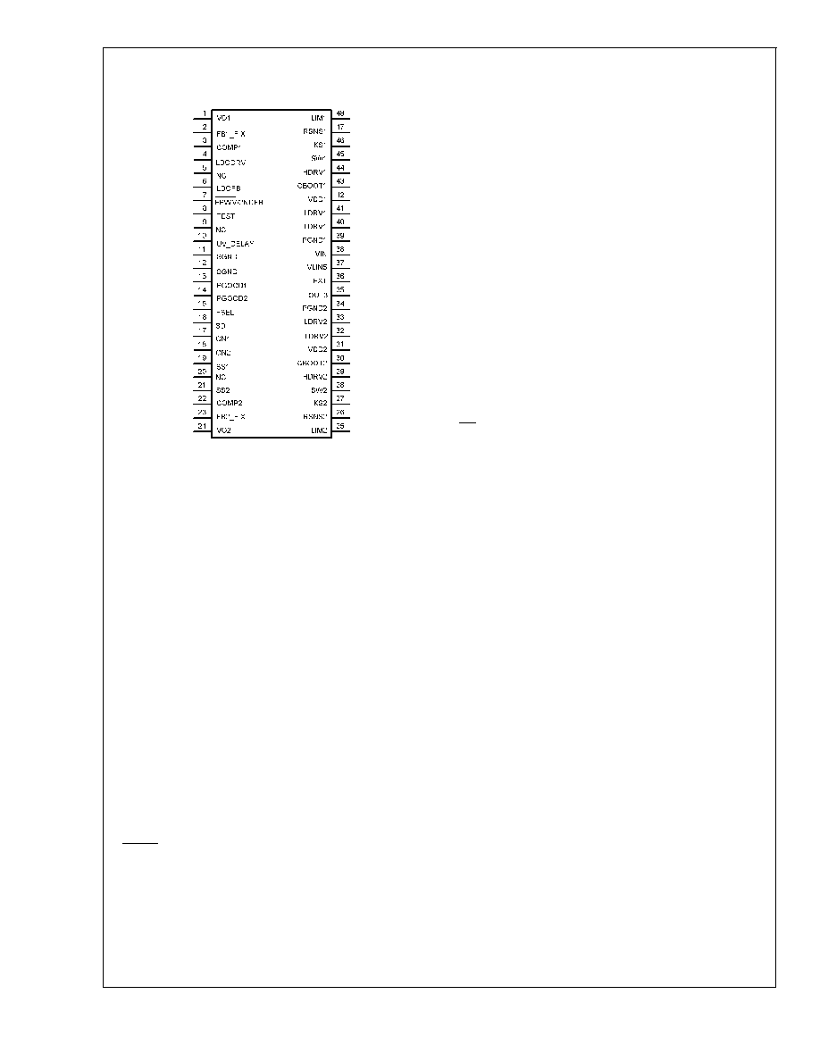
Connection Diagram
TOP VIEW
20015901
48-Lead TSSOP (MTD)
Order Number LM2645MTD
See NS Package Number MTD48
Pin Descriptions
VO1 (Pin 1):The feedback input for Channel 1. Always con-
nect directly to the output. Fixed or adjustable output voltage
is selected by FB1_FIX.
FB1_FIX (Pin 2): The feedback input for setting the output
voltage of Channel 1. Connecting this pin to VLIN5 sets the
output voltage to 5V, or to the center of a voltage divider for
an adjustable output.
COMP1 (Pin 3): Compensation pin for Channel 1. This is the
output of the internal transconductance amplifier. The com-
pensation network should be connected between this pin
and the signal ground, SGND.
LDODRV (Pin 4): The output of the adjustable linear regu-
lator controller. Connects to the base of a PNP Pass transis-
tor. This pin is activated when Channel 1 is enabled.
NC (Pins 5, 9, 20): No internal connection. Connect these
pins to ground.
LDOFB (Pin 6): Dual function input pin. When connected to
the center of a resistor divider, it serves as the 1.238V
feedback input for the LDODRV. Connecting this pin to
VLIN5 disables the LDODRV.
FPWM/2NDFB (Pin 7): Multi-function input pin. When held
HIGH (
>
2V), pulse-skipping mode is enabled for both
switching regulators. When held LOW (
<
0.8V), both regula-
tors will function in Fixed Frequency PWM mode. This pin
can also be connected to the center of a resistor divider for
feedback regulation of a secondary winding voltage. In this
case, Ch 1 will operate in pulse-skipping mode when the
output is lightly loaded. If the linear regulator controller out-
put
is
heavy
loaded,
the
operating
frequency
in
pulse-skipping will be increased accordingly to maintain the
voltage at this pin to 1.5V or higher. Thus, the secondary
winding voltage will always have the necessary overhead
voltage for the linear regulator to maintain regulation.
TEST (Pin 8): Special purpose input pin for factory use only.
This pin must be connected to ground.
UV_DELAY (Pin 10): : A capacitor from this pin to ground
adjusts the delay of the undervoltage protection for the two
switching outputs and the linear regulated output controlled
by the LDODRV. The delay time is set by charging a capaci-
tor to 2.3V from a 5µA current source. Pulling this pin to
ground disables undervoltage protection on these outputs.
SGND (Pin 11,12): Ground connection for the signal level
circuitry. It should be connected to the ground rail of the
system.
PGOOD1 (Pin 13): An open-drain power-good output for
Channel 1. It is 'LOW' (low impedance to ground) whenever
the output voltage travels out of the
±
10% window. It stays
latched in a 'LOW' state if the output travels beyond the
positive limit that trips the over-volatge protection.
PGOOD2 (Pin 14): An open drain power good output for
Channel 2. It serves the same function as the PGOOD1.
FSEL (Pin 15): Selects the Switching Frequency of the two
switching controllers. The frequency is 300kHz when this pin
is pulled HIGH (
>
2V), or 200kHz when this pin is pulled
LOW (
<
0.8V).
SD (Pin 16): Shutdown control input. Pulling this pin LOW
(
<
0.6V) turns OFF the entire chip which then draws less
than 10 µA of supply current. The chip is ON if this pin is held
HIGH (
>
2V). Toggling this pin from HIGH to LOW and then
HIGH again resets the chip causing it to recover from any
protection latch.
ON1 (Pin 17): Output enable for Channel 1 and LDODRV
(Pin 4). Channel 1 and LDODRV are disabled when this pin
is pulled LOW (
<
0.8V), and are enabled when this pin is
pulled HIGH (
>
2V).
ON2 (Pin 18): Output enable for Channel 2. Channel 2 is
enabled when this pin is pulled high (
>
2V) and disabled
when this is pulled low (
<
0.8V).
SS1 (Pin 19): Soft-start input pin for Channel 1. The rise
time of the output voltage of Channel 1 is programmed by
the charge rate of a capacitor connected from this pin to
ground by an internal 2 µA current source. If the output does
not reach regulation (to within -6% of nominal voltage) by
the time this pin exceeds 2V (typical), the UV_DELAY pin
begins charging the capacitor connected from it to ground. If
the output is not within regulation after the UVP delay, the
chip latches off.
SS2 (Pin 21): Soft-start input pin for Channel 2. Serves the
same function as the SS1, Pin 19.
COMP2 (Pin 22): Compensation pin for Channel 2. This is
the output of the internal transconductance amplifier. The
compensation network should be connected between this
pin and the signal ground SGND (Pins 11, 12).
FB2_FIX (Pin 23): The feedback input for setting the output
voltage of Channel 2. Connecting this pin to VLIN5 sets the
output voltage to 3.3V, or to the center of a voltage divider for
an adjustable output.
VO2 (Pin 24): The feedback input for Channel 2. Always
connect directly to the output. Fixed or adjustable output
voltage is selected by FB2_FIX.
ILIM2 (Pin 25): Current limit threshold setting for Channel 2.
It sinks a constant current of 10 µA that is converted to a
voltage through a resistor connected from this pin to Vin. The
voltage across this resistor is compared with either the Vds
LM2645
www.national.com
2

Pin Descriptions
(Continued)
of the top MOSFET or the voltage across an external current
sense resistor to determine if an over-current condition has
occurred in Channel 2.
RSNS2 (Pin 26): The negative (-) Kelvin sense for the
internal current limit comparator of Channel 2. Always use a
separate trace to connect this pin to the current sense point.
Connect this pin to the low side of the current sense resistor
that is placed between V
IN
and the drain of the top MOSFET.
When the Vds of the top MOSFET is used for current sens-
ing, then connect this pin to the source of the top MOSFET.
KS2 (Pin 27): The positive (+) Kelvin sense for the internal
current limit comparator of Channel 2. Use a separate trace
to connect this pin to the current sense point. Connect to Vin
as close to the node of the current sense resistor; when no
current-sense resistor is used, connect it as close to the
Drain node of the upper MOSFET.
SW2 (Pin 28): : Switch-node connection for Channel 2,
which is connected to the source of the top MOSFET. It
serves as the negative supply rail for the topside gate driver,
HDRV2.
HDRV2 (Pin 29): Top-side gate-drive output for Channel 2. A
floating drive output that rides on the switching-node voltage.
CBOOT2 (Pin 30): Bootstrap capacitor connection. It serves
as the positive supply rail for the Channel 2 top-side gate
drive.
VDD2 (Pin 31): The supply rail for the Channel 2 low-side
gate drive, usually ties together with VDD1. Connect to
VLIN5 through a 4.7
resistor and bypassed to ground with
a ceramic capacitor of at least 1µF.
LDRV2 (Pins 32, 33): Low-side gate-drive output for Chan-
nel 2. Tie these two pins together.
PGND2 (Pin 34): Power ground for Channel 2.
OUT3 (Pin 35): The fixed 3.3V linear regulated output. De-
rived from VLIN5 by an internal LDO, it is current limited at
100mA. The continuous output current is a function of the
ambient operating temperature and the total power dissipa-
tion in the chip and must be derated accordingly. See (Note
2) in Electrical Characteristics section.
EXT (Pin 36): External power input to an internal switch.
This pin is usually connected to the fixed 5V output of
Channel 1. When the voltage on this pin is higher than 4.7V,
the internal 5V LDO that provides VLIN5 from VIN is dis-
abled, and an internal switch connects VLIN5 to this pin to
minimize dissipation in the chip. Connect this pin to ground
and VLIN5 to VIN if VIN is operating in 4.5V to 5.5V range.
VLIN5 (Pin 37): This pin is the output of an internal 5V LDO
regulator derived from VIN when no external 5V supply is
available. It supplies the internal bias for the chip, supplies
the boostrap circuitry for gate drive and serves as the input
supply of an internal LDO to generate OUT3. Bypass this pin
to power ground with a minimum of 4.7µF ceramic capacitor.
Connect this pin to the VIN pin when Vin is operating in 4.5V
to 5.5V range.
VIN (Pin 38):The input power of the chip. Connects to the
upper (+) input rail of the system.
PGND1 (Pin 39):Power ground for Channel 1.
LDRV1 (Pins 40, 41): Low-side gate-drive output for Chan-
nel 1. Tie these two pins together.
VDD1 (Pin 42): The supply rail for the low-side gate drive of
Channel 1. Same function as VDD2 (Pin 31).
CBOOT1 (Pin 43): Bootstrap capacitor connection. It serves
as the positive supply rail for the Channel 1 top-side gate
drive.
HDRV1 (Pin 44): Top-side gate-drive output for Channel 1.
See HDRV2 (Pin 29).
SW1 (Pin 45): Switch-node connection for Channel 1, See
SW2 (Pin 28).
KS1 (Pin 46): The upper (+) Kelvin sense for the internal
current limit comparator of Channel 1 (see KS2, Pin 27).
RSNS1 (Pin 47): The lower (-) Kelvin sense for the internal
current limit comparator of Channel 1 (see RSNS2, Pin 26).
ILIM1 (Pin 48): Current limit threshold setting for Channel 1
(see ILIM2, Pin 25).
LM2645
www.national.com
3
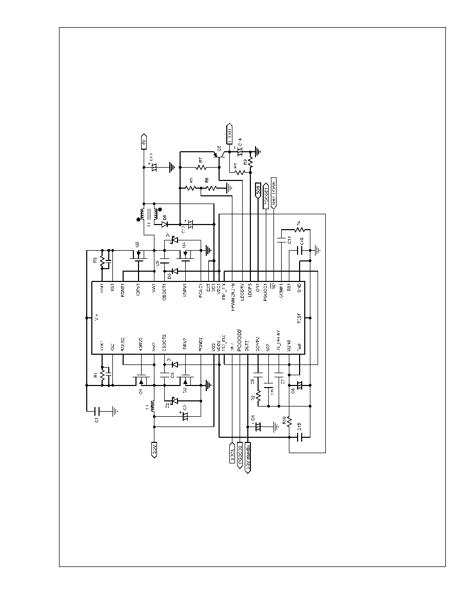
Typical
Application
Circuit
20015902
LM2645
www.national.com
4
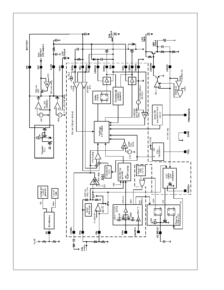
Simplified
Block
Diagram
20015905
LM2645
www.national.com
5
Document Outline