 | ÐлекÑÑоннÑй компоненÑ: LM2648MTD | СкаÑаÑÑ:  PDF PDF  ZIP ZIP |
Äîêóìåíòàöèÿ è îïèñàíèÿ www.docs.chipfind.ru
LM2648
Two-Phase, Synchronous Step-Down 3-Channel
Switching Regulator Controller
General Description
The LM2648 consists of two current mode and two voltage
mode synchronous buck regulator controllers providing 3
outputs at a switching frequency of 300kHz.
Each pair of switching regulator controllers operate 180° out
of phase. This feature reduces the input ripple RMS current,
thereby significantly reducing the required input capacitance.
The two current mode regulator outputs operate as a dual-
phase, single output regulator for high current applications.
Current-mode feedback control on Channel 3 assures supe-
rior line and load regulation and wide loop bandwidth as-
sures excellent response to fast load transients. Channels 1
and 2 employ voltage-mode feedback control.
The LM2648 features analog soft-start circuitry that is inde-
pendent of the output load and output capacitance. This
makes the soft-start behavior more predictable than tradi-
tional soft-start circuits. Sequential startup is built in and
requires a single capacitor to set the timing.
The LM2648 has over-voltage protection and under-voltage
protection for all outputs. Two additional comparator inputs
(analog and logic level) are provided to shut down the IC for
any user defined protection. The FAULT_DELAY pin allows
delayed shut off time for the IC during an under-voltage or
PROT-IN2 fault. The LM2648 also features an adjustable
UVLO feature.
Features
n
Four synchronous buck regulators
n
Channel 3: Two-phase, current mode controller
n
4.5V to 18V input range
n
Built in sequential startup
n
Channels 1 and 2: Independent, 180° out of phase
voltage mode controllers
n
Single soft start for channels 1 and 2
n
Adjustable cycle-by-cycle current limit for each channel
n
Adjustable reference current
n
Adjustable input under-voltage lockout
n
Output over-voltage latch protection
n
Output under-voltage protection with delay
n
Two comparator inputs for user defined protection - one
with delay
n
Thermal shutdown
n
Self-discharge of output capacitors when the regulator is
off
n
TSSOP package
Applications
n
Embedded Computer Systems
n
Interactive Games
n
Set-top Boxes/Home Gateways
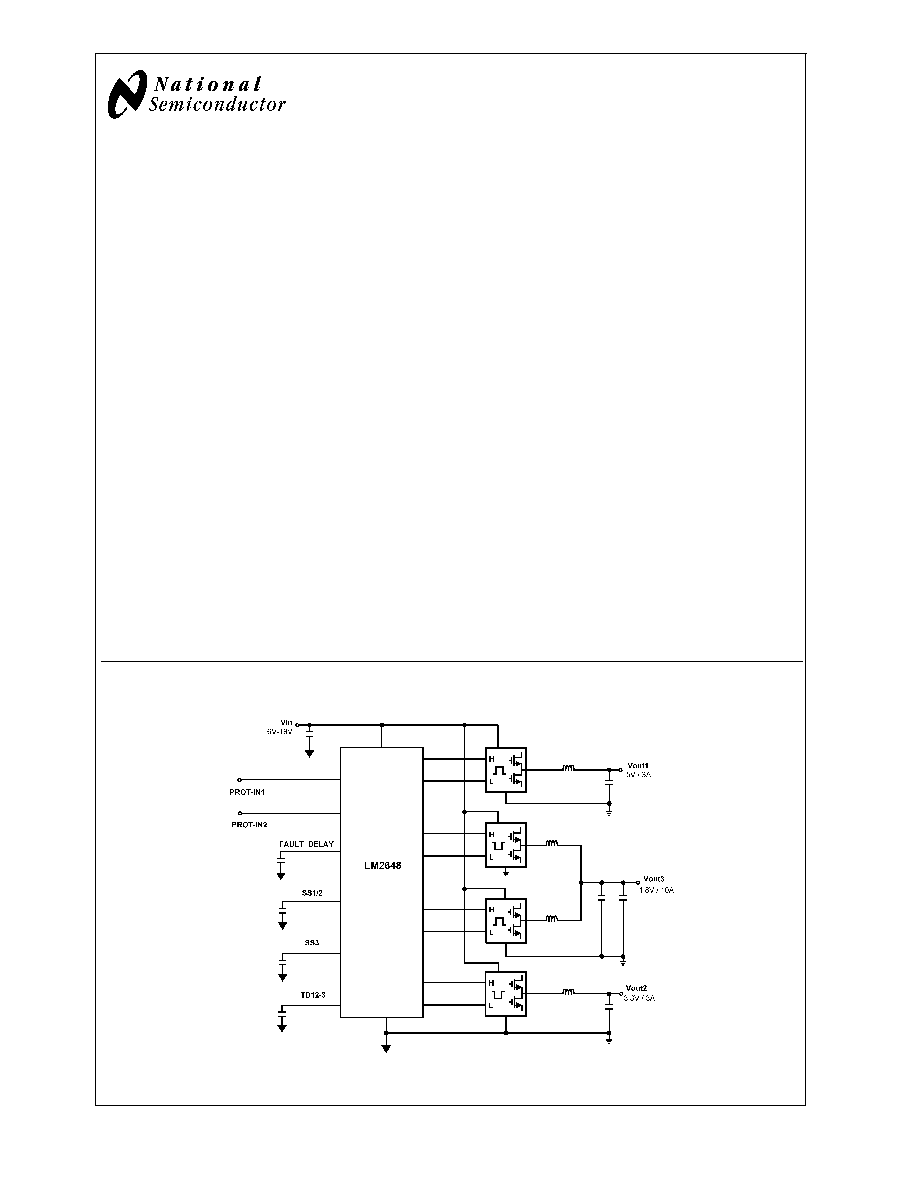
Block Diagram
20059690
December 2004
LM2648
T
wo-Phase,
Synchronous
Step-Down
3-Channel
Switching
Regulator
Controller
© 2004 National Semiconductor Corporation
DS200596
www.national.com
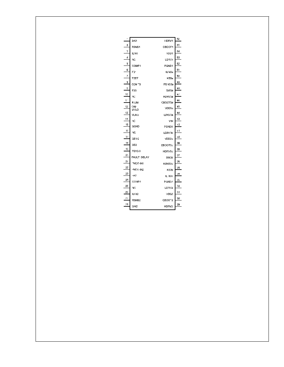
Connection Diagram
TOP VIEW
20059602
56-Lead TSSOP (MTD)
Order Number LM2648MTD
See NS Package Number MTD56
Pin Descriptions
SW1 (Pin 1): Switch-node connection for Channel 1, which
is connected to the source of the top MOSFET of Channel 1.
It serves as the negative supply rail for the top-side gate
drive, HDRV1.
RSNS1 (Pin 2): The negative (-) Kelvin sense for the internal
current limit comparator of Channel 1. Connect this pin to the
low side of the current sense resistor that is placed between
VIN and the drain of the top MOSFET. Always use a sepa-
rate trace to connect this pin.
ILIM1 (Pin 3): Current limit threshold setting for Channel 1. It
sinks a variable current adjusted by RILIM (Pin11), which is
converted to a voltage through a resistor connected from this
pin to the top of the current sense resistor. The voltage
across the resistor is compared with the voltage across the
external current sense resistor to determine if an over-
current condition has occurred on Channel 1.
NC (Pin 4): All NC pins should be connected to SGND.
COMP1 (Pin 5): Compensation pin for Channel 1. This is the
output of the internal error amplifier. The compensation net-
work should be connected between this pin and the feed-
back pin, FB1 (PIN 6).
FB1 (Pin 6): Feedback input for channel 1. Connect to Vout
through a voltage divider to set the channel 1 output voltage.
TEST (Pin 7): Connect to SGND.
COMP3 (Pin 8): Compensation pin for Channel 3. This is the
output of the internal transconductance amplifier. The com-
pensation network should be connected between this pin
and SGND.
FB3 (Pin 9): Feedback input for channel 3. Connect to Vout
through a voltage divider to set the Channel 3 output voltage.
NC (Pin 10): All NC pins should be connected to SGND.
RILIM (Pin 11): Connect a resistor from this pin to SGND to
set the internal ILIM reference current.
ON/UVLO (Pin 12): This is a dual function pin providing
thresholds for user adjustable UVLO and device shutdown.
LM2648
www.national.com
2

Pin Descriptions
(Continued)
Thresholds are 1.2V and 1.9V typical for shutdown and
UVLO respectively. Connect to Vin through a voltage divider
to set the external UVLO threshold.
VLIN5 (Pin 13): The output of the internal 5V LDO regulator
derived from VIN. It supplies the internal bias for the chip and
supplies the bootstrap circuitry for gate drive. Bypass this pin
to signal ground with a minimum of 4.7uF capacitor. VLIN5
should not be used as an external voltage supply.
NC (Pin 14): All NC pins should be connected to SGND.
SGND (Pin 15): The ground connection for the signal-level
circuitry. It should be connected to the ground rail of the
system.
NC (Pin 16): All NC pins should be connected to SGND.
SS1/2 (Pin 17): This pin is the soft start control for channels
1 and 2. Connect a capacitor from this pin to SGND to
control the ramp rate of the output voltage during startup.
SS3 (Pin 18): The soft start pin for channel 3. See Pin 17
(SS1/2).
TD12-3 (Pin 19): Sequential start timing pin. A capacitor
from this pin to ground sets the delay time between channel
1 and 2 and channel 3 entering softstart.
FAULT_DELAY (Pin 20): A capacitor from this pin to ground
sets the delay time for UVP and PROT-IN2 latch off. The
capacitor is charged from a 5uA current source. When the
FAULT_DELAY capacitor charges to 2V (typical), the system
immediately latches off. Connecting this pin to ground will
disable the UVP and PROT-IN2 functions.
PROT_IN1 (Pin 21): A comparator input that latches off all
channels simultaneously when the applied voltage is above
1.239V (typical) voltage level.
PROT_IN2 (Pin 22): A TTL/CMOS compatible input that
activates FAULT_DELAY when the applied voltage is above
a 1.45V typical threshold.
FB2 (Pin 23): Feedback input for channel 2. Connect to Vout
through a voltage divider to set the Channel 2 output voltage.
COMP2 (Pin 24): Compensation pin for Channel 2. This is
the output of the internal error amplifier. The compensation
network should be connected between this pin and the feed-
back pin FB2 (Pin 23).
NC (Pin 25): All NC pins should be connected to SGND.
ILIM2 (Pin 26): Current limit threshold setting for Channel 2.
See ILIM1 (Pin 3).
RSNS2 (Pin 27): The negative (-) Kelvin sense for the
internal current limit comparator of Channel 2. See RSNS1
(Pin 2).
SW2 (Pin 28): Switch-node connection for Channel 2. See
SW1 (Pin1).
HDRV2 (Pin 29): Top-side gate-drive output for Channel 2.
HDRV is a floating drive output that rides on the correspond-
ing SW node voltage.
CBOOT2 (Pin 30): Bootstrap capacitor connection. It serves
as the positive supply rail for the Channel 2 top-side gate
drive. Connect this pin to VDD2 (Pin 31) through a diode,
and connect the low side of the bootstrap capacitor to SW2
(Pin28).
VDD2 (Pin 31): The supply rail for the Channel 2 low-side
gate drive. Connected to VLIN5 (Pin 13) through a 4.7ohm
resistor and bypassed to PGND with a ceramic capacitor of
at least 1uF. Tie all VDDx pins together.
LDRV2 (Pin 32): Low-side gate-drive output for Channel 2.
PGND2 (Pin 33): The power ground connection for channel
2. Connect to the ground rail of the system.
ILIM3b (Pin 34): Current limit threshold setting for Channel
3b. See ILIM1 (Pin 3).
KS3b (Pin 35): The positive (+) Kelvin sense for the internal
current sense amplifier of Channel 3b. Use a separate trace
to connect this pin to the current sense point. It should be
connected to VIN as close as possible to the node of the
current sense resistor.
RSNS3b (Pin 36): The negative (-) Kelvin sense for the
internal current sense amplifier of Channel 3b. See RSNS1
(Pin 2).
SW3b (Pin 37): Switch-node connection for Channel 3b.
See SW1 (Pin1).
HDRV3b (Pin 38): Top-side gate-drive output for Channel
3b. See HDRV2 (Pin 29).
CBOOT3b (Pin 39): Bootstrap capacitor connection. It
serves as the positive supply rail for the Channel 3b top-side
gate drive. See CBOOT2 (Pin 30).
VDD3b (Pin 40): The supply rail for the Channel 3b low-side
gate drive. Tie all VDDx pins together.
LDRV3b (Pin 41): Low-side gate-drive output for Channel
3b.
PGND3 (Pin 42): The power ground connection for channel
3. Connect to the ground rail of the system.
VIN (Pin 43): The power input pin for the chip. Connect to
the positive (+) input rail of the system. Bypass to PGND with
a 1uF capacitor.
LDRV3a (Pin 44): Low-side gate-drive output for Channel
3a.
VDD3a (Pin 45): The supply rail for the Channel 3a low-side
gate drive. Tie all VDDx pins together.
CBOOT3a (Pin 46): Bootstrap capacitor connection. It
serves as the positive supply rail for the Channel 3a top-side
gate drive. See CBOOT2 (Pin 30).
HDRV3a (Pin 47): Top-side gate-drive output for Channel
3a. See HDRV2 (Pin 29).
SW3a (Pin 48): Switch-node connection for Channel 3a.
See SW1 (Pin1).
RSNS3a (Pin 49): The negative (-) Kelvin sense for the
internal current sense amplifier of Channel 3a. See RSNS1
(Pin 2).
KS3a (Pin 50): The positive (+) Kelvin sense for the internal
current sense amplifier of Channel 3a. See KS3b (Pin 35).
ILIM3a (Pin 51): Current limit threshold setting for Channel
3a. See ILIM1 (Pin 3).
PGND1 (Pin 52): The power ground connection for channel
1. Connect to the ground rail of the system.
LDRV1 (Pin 53): Low-side gate-drive output for Channel 1.
VDD1 (Pin 54): The supply rail for the Channel 1 low-side
gate drive. Tie all VDDx pins together.
CBOOT1 (Pin 55): Bootstrap capacitor connection. It serves
as the positive supply rail for the Channel 1 top-side gate
drive. See CBOOT2 (Pin 30).
HDRV1 (Pin 56): Top-side gate-drive output for Channel 1.
See HDRV2 (Pin 29).
LM2648
www.national.com
3
Absolute Maximum Ratings
(Note 1)
If Military/Aerospace specified devices are required,
please contact the National Semiconductor Sales Office/
Distributors for availability and specifications.
Voltages from the indicated pins to SGND/PGND:
VIN, ILIMx, KS3a, KS3b
-0.3V to 20V
SWx, RSNSx
-0.3V to (VIN +
0.3)V
FB1, FB2, FB3x, VDDx,ON/UVLO
-0.3V to 7V
COMPx, FAULT_DELAY, SSx
-0.3V to (VLIN5 +
0.3)V
CBOOT1 to SW1, CBOOT2 to SW2,
CBOOT3x to SW3x
-0.3V to 7V
LDRV1, LDRV2, LDRV3x
-0.3V to
(VDD+0.3)V
HDRV1 to SW1, HDRV2 to SW2,
HDRV3x to SW3x
-0.3V
HDRV1 to CBOOT1, HDRV2 to
CBOOT2, HDRV3x to CBOOT3x
0.3V
Power Dissipation (T
A
= 25°C),
(Note 2)
1.3W
Ambient Storage Temperature
Range
-65°C to +150°C
Soldering Dwell Time, Temperature
(Note 3)
Infrared
Vapor Phase
10-20sec, 240°C
75sec, 219°C
ESD Rating (Note 4)
2kV
Operating Ratings
(Note 1)
VIN (VIN and VLIN5 separate)
5.5V to 18V
VIN (VIN tied to VLIN5)
4.5V to 5.5V
Junction Temperature
0°C to +125°C
Electrical Characteristics
Unless otherwise specified, V
IN
= 12V, SGND = PGND = 0V, VLIN5 = VDD1 = VDD2 = VDD3x. Limits appearing in boldface
type apply over the full operating junction temperature range. Specifications appearing in plain type are measured using low
duty cycle pulse testing with T
A
= 25°C (Note 5), (Note 6). Min/Max limits are guaranteed by design, test, or statistical analysis.
Symbol
Parameter
Conditions
Min
Typ
Max
Units
System
V
OUT
/V
OUT
Load Regulation
VIN = 12V, V
comp1, 2
= 1V to 3V,
V
comp3
= 0.5V to 1.5V
.04
%
V
OUT
/V
OUT
Line Regulation
5.5V
VIN 18V, V
compx
=1.25V
.04
%
V
FB1
, V
FB2
Feedback Voltage
5.5V
VIN 18V
1.218
1.239
1.260
V
V
FB3
Feedback Voltage
5.5V
VIN 18V
1.220
1.241
1.262
V
I
VIN
Input Supply Current
V
ON/UVLO
>
2.25V (not switching)
5.5V
VIN 18V
1.66
2.2
mA
Standby
1.5V
<
V
ON/UVLO
<
1.7V
Shutdown (Note 7)
V
ON/UVLO
= 0V
45
120
µA
VLIN5
VLIN5 Output Voltage
IVLIN5 = 0 to 50mA,
7V
VIN 18V
4.65
5.0
5.35
V
Current Limit
V
Clos1, 2, 3
Current Limit
Comparator Offset
(V
ILIMX
-V
RSNSX
)
0
±
7.0
mV
V
CLx1, 2, 3
Current Limit Sink
Current
R
ILIM
= 1.238/20µA
18.2
20
21.8
µA
V
RILIM
ILIM Reference Voltage
1.238
V
Soft Start
I
ss1/2_SC
Soft-Start Source
Current
V
ss
= 1V
0.5
2.05
3.8
µA
I
ss3_SC
Soft-Start Source
Current
V
ss
= 1V
0.5
2.05
3.8
µA
I
ss1/2_SK
Soft-Start Sink Current
V
ss1/2, 3
= 1V, ON/UVLO = 1.6V
2
4.9
9
µA
I
ss3_SK
Soft-Start Sink Current
V
ss1/2, 3
= 1V, ON/UVLO = 1.6V
2
5.0
9
µA
I
SC_TD12-3
Delay Timer Source
Current
V
TD
= 1.5V
6.2
9.8
13.2
µA
LM2648
www.national.com
4
Electrical Characteristics
(Continued)
Unless otherwise specified, V
IN
= 12V, SGND = PGND = 0V, VLIN5 = VDD1 = VDD2 = VDD3x. Limits appearing in boldface
type apply over the full operating junction temperature range. Specifications appearing in plain type are measured using low
duty cycle pulse testing with T
A
= 25°C (Note 5), (Note 6). Min/Max limits are guaranteed by design, test, or statistical analysis.
Symbol
Parameter
Conditions
Min
Typ
Max
Units
I
SK_TD12-3
Delay Timer Sink
Current
V
TD
= 0.4V
192
274
356
µA
V
TD12-3
Delay Timer Threshold
Voltage
Rising
1.70
1.94
2.20
V
I
ss1/2_sc
/
I
ss3_sc
Soft-Start Source
Current Ratio
-13%
1.0
+13%
A/A
I
ss1/2_sc
/
I
sc_TD12-3
Soft-Start to Delay Timer
Source Current Ratio
-32%
0.209
+32%
A/A
Shutdown
V
Standby
Standby Threshold
(ON/UVLO pin)
Rising
Shutdown to Standby
0.95
1.2
1.44
V
Hysteresis
149
mV
V
ON
ON Threshold
(ON/UVLO pin)
Rising
Standby to On
1.75
1.98
2.20
V
Hysteresis
205
mV
S
W_ R1, 2
SW1, 2 ON Resistance
V
SW1
= V
SW2
= 0.4V
440
570
700
S
W_R3a, 3b
SW3a, 3b ON
Resistance
V
SW3a
= V
SW3b = 0.4V
200
249
310
V
SW_dis
SW3a Quick Discharge
Threshold at FB3 (falling
edge)
LDRV3a = High
.81
V
Protection
I
SC_FAULTDELAY
FAULT_DELAY source
current
FAULT_DELAY = 2.0V
3.54
4.7
5.9
µA
I
SK_FAULTDELAY
FAULT_DELAY sink
current
FAULT_DELAY = 0.4V
0.27
mA
V
FAULT_DELAY
FAULT_DELAY
threshold Voltage
Rising
1.75
1.96
2.20
V
V
UVP
FB1, 2, 3 Under Voltage
Protection Latch
Threshold
As a percentage of nominal output
voltage (falling edge)
75
80.6
86
%
Hysteresis
4
%
V
OVP
FB1, 2, 3 Over-voltage
Shutdown Latch
Threshold
As a percentage of nominal output
voltage (rising edge)
106
112
119
%
V
UVLO_INT
VLIN5 Under Voltage
Lockout Threshold
Rising
4.2
V
Hysteresis
8
%
V
PROT-IN1
Analog protection
threshold
1.19
1.239
1.4
V
V
PROT-IN2
Logic protection
threshold
0.8
1.48
2
V
I
sk_prot-in2
PROT-IN2 sink current
2
µA
Gate Drive
I
CBOOT
CBOOTx Leakage
Current
V
CBOOTX
= 7V
10
nA
I
SC_DRV
HDRVx and LDRVx
Source Current
HDRV = LDRV = 2.5V
0.5
A
I
sk_HDRV
HDRVx Sink Current
HDRVX = 2.5V
0.8
A
LM2648
www.national.com
5
Document Outline