LM2652
1.5A, Dual High Performance Synchronous Buck
Regulator
General Description
The LM2652 is a monolithic dual synchronous buck regula-
tor designed for low output voltages. Special attention to
power sequencing, voltage accuracy and start-up character-
istics has been made to enable a simple solution to the
challenging requirements of FPGA & DSP power. Four inte-
grated FET power switches ensure high efficiency, minimal
external components and maximum ease-of-use. The IC can
accept an input of 2.7V to 5.5V and deliver 1.5A per channel.
The bias and power inputs can run from different rails to
balance system power. Output voltages are factory program-
mable from 0.8V to 3.3V in 50mV steps. The LM2652 is
available in two switching frequency options (650kHz and
1300kHz) and both options can be synchronized to an ex-
ternal clock of 300-1600kHz. The two switching channels run
180∞ out of phase to reduce input capacitor size and cost.
Output fault protection is provided by the use of cycle-by-
cycle current limit and frequency fold-back. Separate soft-
start, power good flags and output enables allow for power
sequencing flexibility.
Features
n
Dual 1.5 Amp outputs
n
Output voltage factory set in 50mV steps from 0.8V to
3.3V
n
Input voltage from 2.7V to 5.5V
n
2% reference accuracy
n
4 internal 80m
synchronous switches
n
180∞ out of phase operation
n
Independent enables (CMOS compatible)
n
Separate Power Good flags
n
650kHz or 1300kHz switching frequency
n
PLL synchronization to an external clock
n
Programmable soft-start
n
Supports all-ceramic output capacitors
n
TSSOP-28 Exposed Pad package
n
Current limit and thermal shutdown protection
Applications
n
Cable Modems
n
xDSL Modems
n
DSP, FPGA and microprocessor power
n
Local Regulation
n
Set-Top Box
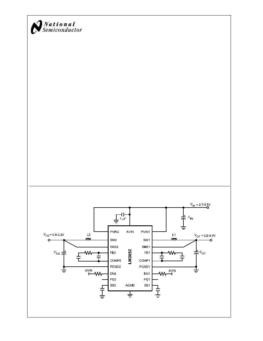
Typical Application
20117201
ADVANCE INFORMATION
January 2005
LM2652
1.5A,
Dual
High
Performance
Synchronous
Buck
Regulator
© 2005 National Semiconductor Corporation
DS201172
www.national.com
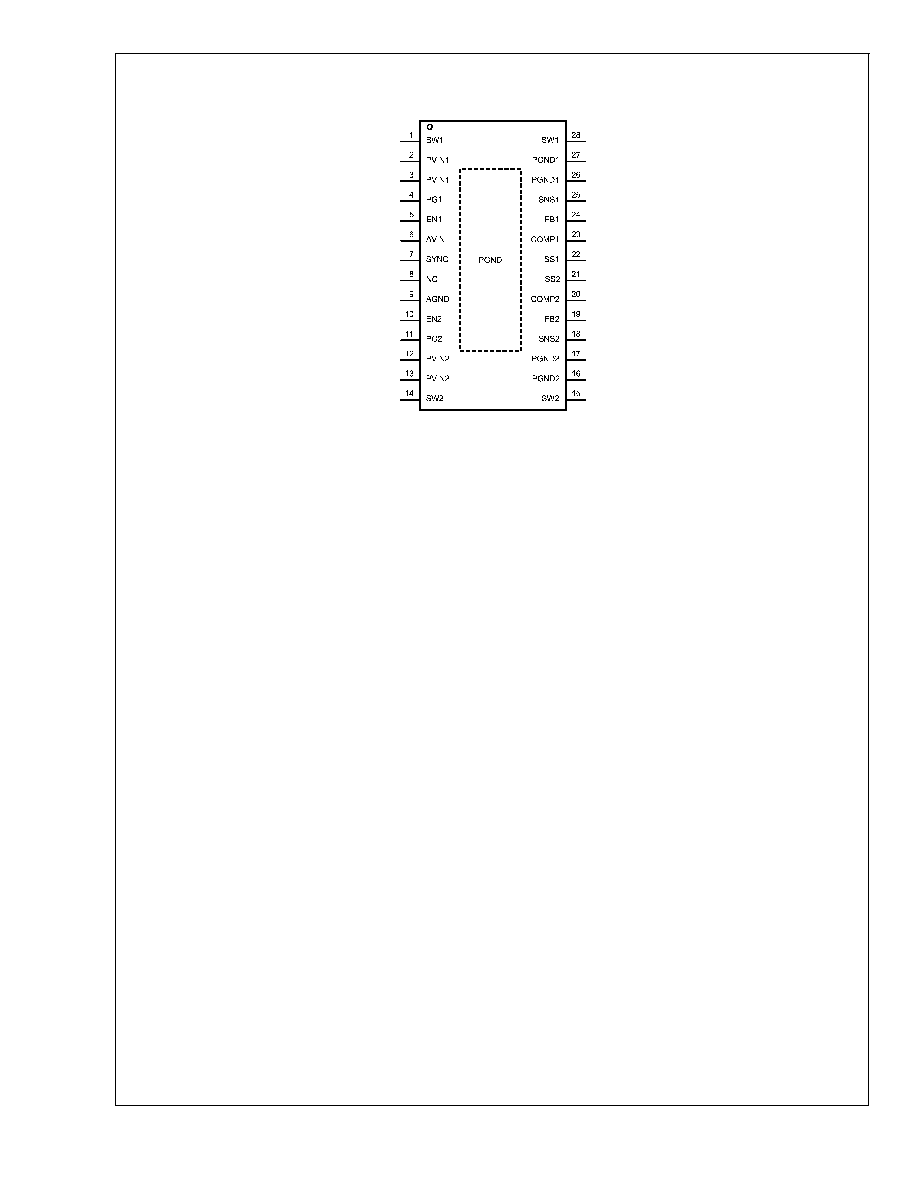
Connection Diagram
TOP VIEW
20117202
28-Lead Plastic (TSSOP Exposed Pad)
See NS Package Number MXA28A
Pin Descriptions
SW1 (Pins 1, 28): The switch node pins for Channel 1.
Connect the Channel 1 output inductor to these pins.
PVIN1 (Pins 2, 3): Input voltage supply for the Channel 1
switch. In a split-rail system, this supply should not exceed
the voltage at the AVIN pin.
PG1 (Pin 4): Open drain Power Good flag for Channel 1.
When this pin voltage is high, the output voltage is ready to
deliver power to the load. Connect to AVIN through a 10k
pull-up resistor.
EN1 (Pin 5): Channel 1 logic enable. Input to a CMOS
Schmitt trigger. Set this input high for normal operation.
When low, Channel 1 is in shutdown mode. Connect to
ground through a 100k
pull-down resistor.
AVIN (Pin 6): Power supply for the system. Bypass this pin
with a small (0-10
, 1 µF) filter if it is connected to the same
rail as PVIN.
SYNC (Pin 7): PWM frequency adjust. Connect a PWM
clock to this pin. If unused, connect this pin to ground.
NC (Pin 8): No internal connection. This pin should be
connected to ground.
AGND (Pin 9): Ground pin for the signal level circuitry. Must
be connected to the system ground.
EN2 (Pin 10): Channel 2 logic enable. Input to a CMOS
Schmitt trigger. Set this input high for normal operation.
When low, Channel 2 is in shutdown mode. Connect to
ground through a 100k
pull-down resistor
PG2 (Pin 11): Open drain Power Good flag for Channel 2.
When this pin level is high, the Output voltage is ready to
deliver power to the load. Connect to AVIN through a 10k
pull-up resistor.
PVIN2 (Pin 12,13): Input voltage supply for the Channel 2
switch. In a split-rail system, this supply should not exceed
the voltage at the AVIN pin.
SW2 (Pin 14, 15): The switch node pins for Channel 2.
Connect the Channel 2 output inductor to these pins.
PGND2 (Pin 26, 27): Ground pins for the high current cir-
cuitry. Must be connected to the system ground.
SNS2 (Pin 18): The output voltage (V
O
) sense pin for Chan-
nel 2. Connect this pin directly to the load.
FB2 (Pin 19): The input to the error amplifier of Channel 2.
COMP2 (Pin 20): The output of the Channel 2 error ampli-
fier.
SS2 (Pin 21): Soft start pin for Channel 2. Connect a small
capacitor to this pin to control the slew rate of V
O2
during
start-up.
SS1 (Pin 22): Soft start pin for Channel 1. Connect a small
capacitor to this pin to control the slew rate of V
O1
during
start-up.
COMP1 (Pin 23): The output of the Channel 1 error ampli-
fier.
FB1 (Pin 24): The input to the error amplifier of Channel 1.
SNS1 (Pin 25): The output voltage (V
O
) sense pin for Chan-
nel 1. Connect this pin directly to the load.
PGND2 (Pins 16, 17): Ground pins for the high current
circuitry. Must be connected to the system ground.
EXPOSED PAD: Connect to power ground.
LM2652
www.national.com
2
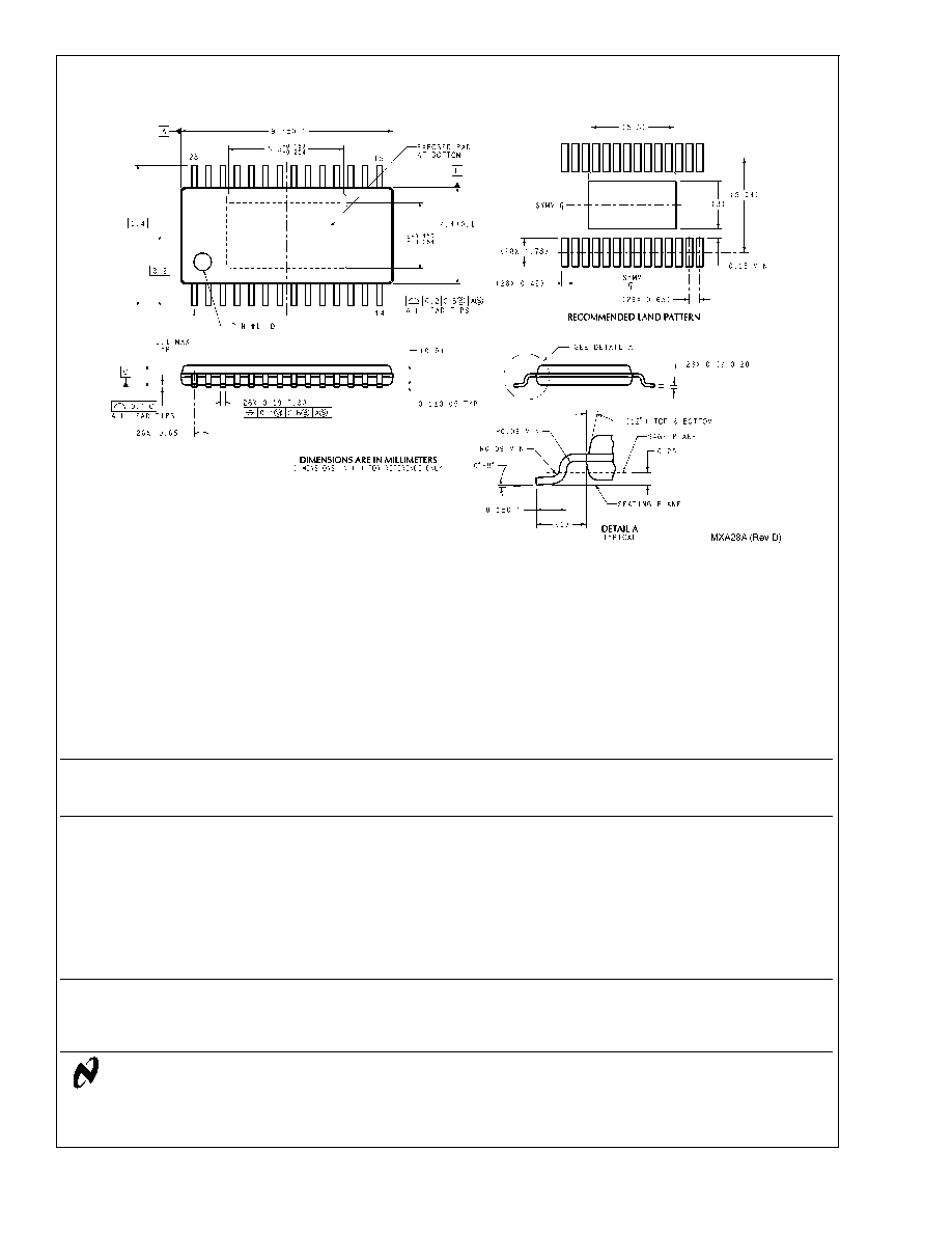
Physical Dimensions
inches (millimeters)
unless otherwise noted
28-Lead Plastic (TSSOP Exposed Pad)
Order Number LM2652MTC
NS Package Number MXA28A
National does not assume any responsibility for use of any circuitry described, no circuit patent licenses are implied and National reserves
the right at any time without notice to change said circuitry and specifications.
For the most current product information visit us at www.national.com.
LIFE SUPPORT POLICY
NATIONAL'S PRODUCTS ARE NOT AUTHORIZED FOR USE AS CRITICAL COMPONENTS IN LIFE SUPPORT DEVICES OR SYSTEMS
WITHOUT THE EXPRESS WRITTEN APPROVAL OF THE PRESIDENT AND GENERAL COUNSEL OF NATIONAL SEMICONDUCTOR
CORPORATION. As used herein:
1. Life support devices or systems are devices or systems
which, (a) are intended for surgical implant into the body, or
(b) support or sustain life, and whose failure to perform when
properly used in accordance with instructions for use
provided in the labeling, can be reasonably expected to result
in a significant injury to the user.
2. A critical component is any component of a life support
device or system whose failure to perform can be reasonably
expected to cause the failure of the life support device or
system, or to affect its safety or effectiveness.
BANNED SUBSTANCE COMPLIANCE
National Semiconductor certifies that the products and packing materials meet the provisions of the Customer Products Stewardship
Specification (CSP-9-111C2) and the Banned Substances and Materials of Interest Specification (CSP-9-111S2) and contain no ``Banned
Substances'' as defined in CSP-9-111S2.
National Semiconductor
Americas Customer
Support Center
Email: new.feedback@nsc.com
Tel: 1-800-272-9959
National Semiconductor
Europe Customer Support Center
Fax: +49 (0) 180-530 85 86
Email: europe.support@nsc.com
Deutsch Tel: +49 (0) 69 9508 6208
English
Tel: +44 (0) 870 24 0 2171
FranÁais Tel: +33 (0) 1 41 91 8790
National Semiconductor
Asia Pacific Customer
Support Center
Email: ap.support@nsc.com
National Semiconductor
Japan Customer Support Center
Fax: 81-3-5639-7507
Email: jpn.feedback@nsc.com
Tel: 81-3-5639-7560
www.national.com
LM2652
1.5A,
Dual
High
Performance
Synchronous
Buck
Regulator